

Vectron International, 267 Lowell Rd, Hudson NH 03051-4916 Tel: 1-88-VECTRON-1 Website: www.vectron.com
Page 1 of 8 Rev: 14Nov03
VS-500
Voltage Controlled SAW Oscillator
Features
• Improved High Performance ASIC
• Industry Standard Package, 9 x 14 x 4.5 mm
• Output Frequencies from 155 MHz to 850 MHz
• 3.3 V or 5.0 V Operation
• At 155.52 MHz, Jitter < 0.50 ps-rms (12 kHz to 20 MHz)
• At 622.08 MHz, Jitter < 0.30 ps-rms (50 kHz to 80 MHz)
• LV-PECL, PECL, or ECL Configurations
• Complementary Outputs
• Output Disable Feature
Applications
PLL circuits for Clock Smoothing and Frequency Translation
Description Standard
• 10G Fibre Channel INCITS/T11 Project 1413-D
• 10GbE LAN / WAN IEEE 802.3ae
• OC-192 ITU-T G.709
• SONET / SDH GR-253-CORE Issue3
Description
The VS-500 is a SAW based voltage controlled oscillator that
operates at the fundamental frequency of the internal SAW filter.
This resonator is a high Q quartz device that enables the circuit
to achieve low phase jitter performance over a wide operating
temperature range. The oscillator is housed in a hermetically
sealed J-lead surface mount package offered on tape and reel.
It has an output disable to facilitate on-board testing.
Vcc COutput Output
GndODVc
SAW
查询VS-500-KEF-GNN669.6429供应商
VS-500 Voltage Controlled SAW Oscillator
Vectron International, 267 Lowell Rd, Hudson NH 03051-4916 Tel: 1-88-VECTRON-1 Website: www.vectron.com
Page 2 of 8 Rev: 14Nov03
Electrical Performance
Parameter Symbol Minimum Typical Maximum Units Notes
Frequency
Nominal Frequency
Absolute Pull Range
Linearity
Gain Transfer @ 155.52 MHz (See Pg 5/6)
Gain Transfer @ 622.08 MHz (See Pg 5/6)
Temperature Stability @ 155.52 MHz
Temperature Stability @ 622.08 MHz
f
N
APR
Lin
K
V
K
V
f
STAB
f
STAB
±50
150 - 850
±5
+691/+435
+434/+281
±100
±150
MHz
ppm
%
ppm/V
ppm/V
ppm
ppm
1,2,3
1,2,3,9/10
2,4,9/10
2,9/10
2,9/10
1,6
1,6
Supply
Voltage
Current (No Load)
V
CC
ICC
2.97/4.5
3.3/5.0
55
3.63/5.5
80
V
mA
2,3
3
Outputs
Mid Level
Swing
Current
Rise & Fall Time
Symmetry
Spurious Suppression
Jitter @ 155.52 MHz (See Pg 5/6)
Jitter @ 622.08 MHz (See Pg 5/6)
I
OUT
tR, tF
SYM
φJ
φJ
VCC-1.5
45
50
VCC-1.3
850
250
50
60
0.440
0.230
VCC-1.1
20
400
55
V
mV-pp
mA
ps
%
dBc
ps-rms
ps-rms
2,3
2,3
6
5,6
2,3
6
6,7
6,8
Control Voltage
Input Impedance (LV-PECL or PECL)
Input Impedance (ECL)
Modulation Bandwidth
Z
c
Z
c
BW
100
10
500
kΩ
kΩ
kHz
6
6
6
Operating Temperature TOP -40 85 °C 1,3
Package Size 9.0 x 14.0 x 4.5 mm
1. See Standard Frequencies and Ordering Information (Pg 8).
2. Parameters are tested with production test circuit below (Fig 2).
3. Parameters are tested at ambient temperature with test limits guardbanded for specified operating temperature.
4. Measured as the maximum deviation from the best straight-line fit, per MIL-0-55310.
5. Measured from 20% to 80% of a full output swing (Fig 1).
6. Not tested in production, guaranteed by design, verified at qualification.
7. Integrated across 12 kHz to 20 MHz, per GR-253-CORE Issue3.
8. Integrated across 50 kHz to 80 MHz, per GR-253-CORE Issue3.
9. Tested with Vc = 0.3V to 3.0V.
10. Tested with Vc = 0.5V to 4.5V.
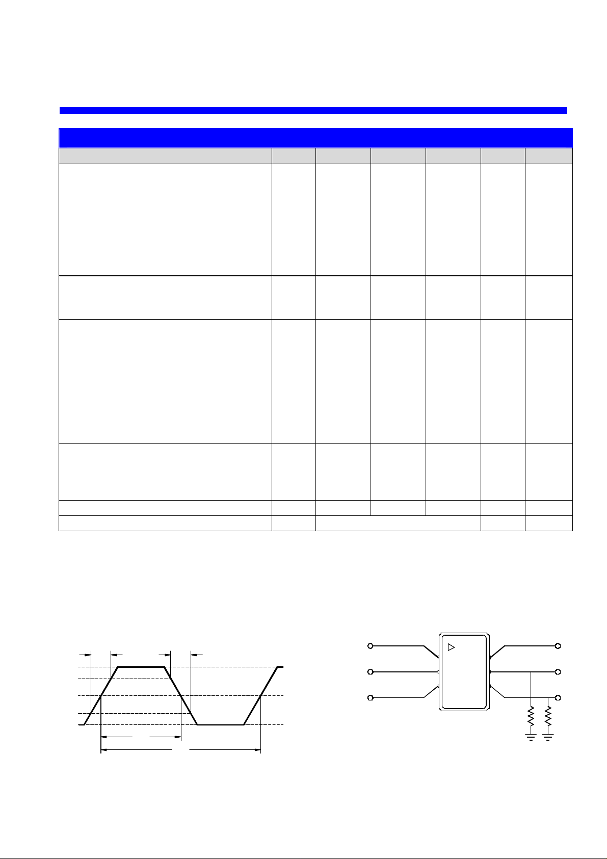
Figure 1. 10K LV-PECL Waveform Figure 2. 3.3V Test Circuit
Vcc - 1.6V
Vcc - 1.3V
Vcc - 1.0V
80%
20%
t t t t SYM = 100 x t
/ t
2 5
50Ω50Ω
Test Circuit Notes:
1) To Permit 50Ω Measurement of Outputs, all DC Inputs are Biased Down 1.3V.
2) All Voltage Sources Contain Bypass Capacitors to Minimize Supply Noise.
3) 50Ω Terminations are Within Test Equipment.
(-1.3V to +2V)
(-1.3V, Open)
(-1.3V)
(+2V)
COutput
Output
Disable, Enable
1 6
3 4
VS-500 Voltage Controlled SAW Oscillator
Vectron International, 267 Lowell Rd, Hudson NH 03051-4916 Tel: 1-88-VECTRON-1 Website: www.vectron.com
Page 3 of 8 Rev: 14Nov03
8.89±0.15
[0.350±0.006]
13.97±0.20
[0.550±0.008]
0.46±0.05
[0.018±0.002]
2.54±0.13
[0.100±0.005] 5.08±0.13
[0.200±0.005]
4.49
+0.20
-0.30
[0.177
+0.008
-0.012 ]
mm
[inch]
7.63
[0.300]
VS-500-LFF-GNN
XXX.XXX
VI YWW
1
43625
Outline Diagram Pad Layout
Pin Out
Pin
Symbol
Function
1 VC VCSO Control Voltage
2
OD Output Disable*
Disabled = LV-CMOS Logic 0 (or GND)
Enabled = LV-CMOS Logic 1 (or Open)
3 GND Case and Electrical Ground
4 Output VCSO Output
5 COutput VCSO Complementary Output
6 VCC Power Supply Voltage (3.3V / 5.0V ±10%)
*For 5.0V Operation, CMOS Levels Should Be Applied.
Tape and Reel (EIA-481-2-A)
Tape Dimensions (mm) Reel Dimensions (mm)
Dimension W F Do Po P1 A B C D N W1 W2 # Per
Tolerance Typ Typ Typ Typ Typ Typ Min Typ Min Min Typ Max
Reel
VS-500 24 11.5 1.5 4 12 330 1.5 13 20.2 100 24.4 30.4 200
Po
W
AN
F
P1
W1
W2
C
B
D
ØDo
mm
[inch]
8.80
[0.346]
1.27
[0.050]
2.54
[0.100]
5.08
[0.200]
3.00
[0.118]

VS-500 Voltage Controlled SAW Oscillator
Vectron International, 267 Lowell Rd, Hudson NH 03051-4916 Tel: 1-88-VECTRON-1 Website: www.vectron.com
Page 4 of 8 Rev: 14Nov03
Absolute Maximum Ratings
Parameter Symbol Ratings Unit
Power Supply VCC 0 to 6 V
Output Current Iout 25 mA
Voltage Control Range VC 0 to VCC V
Storage Temperature TS -55 to 125
°C
Soldering Temp/Time TLS 220/10
°C/sec
Stresses in excess of the absolute maximum ratings can permanently damage the device. Functional operation is
not implied at these or any other conditions in excess of conditions represented in the operational sections of this
datasheet. Exposure to absolute maximum ratings for extended periods may adversely affect device reliability.
Suggested Output Load Configurations (3.3V Operation)
LV-PECL to LV-PECL: For short transmission lengths, the power
consumption could be reduced by removing the 100Ω resistor and
doubling the value of the pull down resistors.
Functional Test: Allows standard power supply configuration.
Since AC coupled, the LV-PECL levels cannot be measured.
LV-PECL to LVDS: Restricted for short transmission lengths.
Configuration may require modification depending on LVDS receiver.
40Ω 40Ω
150Ω
150Ω
49Ω 49Ω
+3.3V
Production Test: Allows direct DC coupling into 50Ω measurement
equipment. Must bias the power supplies as shown. Similar to Figure 1.
0.01 µF
0.01 µF
1 6
2
3 4
5
Vc
OD
Gnd
+3.3V
0.01 µF
0.10 µF
Vcc
COutput
240Ω
Output
240Ω
100Ω
Z = 50Ω
Z = 50Ω
OutputGnd
3 4
Z = 50Ω
+3.3V
0.10 µF
OD
Vc
61
2 5
COutput
Vcc
0.01 µF
Z = 50Ω
Gnd
OD
Vc
43
Output
240Ω
1 6
2 5
COutput
Vcc
0.01 µF
+3.3V
0.10 µF
240Ω
-1.3V
OD
Vc
3 4
61
2 5
COutput
Output
Vcc
+2.0V
0.01 µF
0.10 µF

VS-500 Voltage Controlled SAW Oscillator
Vectron International, 267 Lowell Rd, Hudson NH 03051-4916 Tel: 1-88-VECTRON-1 Website: www.vectron.com
Page 5 of 8 Rev: 14Nov03
y = 691.39x - 1010.34
y = 433.82x - 606.16
-900
-800
-700
-600
-500
-400
-300
-200
-100
0
100
200
300
400
500
600
700
800
900
1000
1100
0.3 0.6 0.9 1.2 1.5 1.8 2.1 2.4 2.7 3
Control Voltage (V)
Frequency (PPM)
155_3V Vc Pull
622_3V Vc Pull
Linear (155_3V Vc Pull)
Linear (622_3V Vc Pull)
Typical Characteristics (3.3V Operation)
Vc Pull Characteristics (22.5 oC)
Typical Gain Transfer @ 155.52 = +691 ppm/V
Typical Gain Transfer @ 622.08 = +434 ppm/V
Calculated Jitter @ 155.52 MHz (22.5 oC)
SONET OC-48 (12kHz-20MHz) = 0.442 ps-rms; 3.09 ps-pp
SONET OC-192 (50kHz-80MHz) = 0.685 ps-rms; 4.80 ps-pp
Calculated Jitter @ 622.08 MHz (22.5 oC)
SONET OC-48 (12kHz-20MHz) = 0.244 ps-rms; 1.71 ps-pp
SONET OC-192 (50kHz-80MHz) = 0.214 ps-rms; 1.50 ps-pp

VS-500 Voltage Controlled SAW Oscillator
Vectron International, 267 Lowell Rd, Hudson NH 03051-4916 Tel: 1-88-VECTRON-1 Website: www.vectron.com
Page 6 of 8 Rev: 14Nov03
y = 435.42x - 979.81
y = 281.23x - 597.87
-900
-800
-700
-600
-500
-400
-300
-200
-100
0
100
200
300
400
500
600
700
800
900
1000
1100
0.5 1 1.5 2 2.5 3 3.5 4 4.5
Control Voltage (V)
Frequency (PPM)
155_5V Vc Pull
622_5V Vc Pull
Linear (155_5V Vc Pull)
Linear (622_5V Vc Pull)
Typical Characteristics (5.0V Operation)
Vc Pull Characteristics (22.5 oC)
Typical Gain Transfer @ 155.52 = +435 ppm/V
Typical Gain Transfer @ 622.08 = +281 ppm/V
Calculated Jitter @ 155.52 MHz (22.5 oC)
SONET OC-48 (12kHz-20MHz) = 0.418 ps-rms; 2.93 ps-pp
SONET OC-192 (50kHz-80MHz) = 0.656 ps-rms; 4.59 ps-pp
Calculated Jitter @ 622.08 MHz (22.5 oC)
SONET OC-48 (12kHz-20MHz) = 0.215 ps-rms; 1.51 ps-pp
SONET OC-192 (50kHz-80MHz) = 0.226 ps-rms; 1.58 ps-pp

VS-500 Voltage Controlled SAW Oscillator
Vectron International, 267 Lowell Rd, Hudson NH 03051-4916 Tel: 1-88-VECTRON-1 Website: www.vectron.com
Page 7 of 8 Rev: 14Nov03
Reliability
The VS-500 family is capable of meeting the following qualification tests:
Environmental Compliance
Parameter Conditions
Mechanical Shock MIL-STD-883, Method 2002
Mechanical Vibration MIL-STD-883, Method 2007
Solderability MIL-STD-883, Method 2003
Gross and Fine Leak MIL-STD-883, Method 1014
Resistance to Solvents MIL-STD-883, Method 2016
Handling Precautions
Although ESD protection circuitry has been designed into the VS-500 proper precautions should be taken when
handling and mounting. VI employs a human body model and a charged-device model (CDM) for ESD
susceptibility testing and design protection evaluation.
ESD Ratings
Model Minimum Conditions
Human Body Model 1500 V MIL-STD 883, Method 3015
Charged Device Model 1000 V JESD 22-C101
Recommended Solder Reflow Profile
VI qualification includes aging at various extreme temperatures, shock and vibration, temperature cycling, and IR
reflow simulation. The conditions a device can withstand are well understood and devices can be subjected to the
profile above. This profile shows a ramp up condition to prevent thermal shock, a preheat period in which the flux
is activated, a ramp up to 183°C which is the reflow temperature of Sn/Pb eutectic, and a gradual cool down. The
time above 183°C should not exceed 60 seconds and the peak temperature should be no more than 220°C for 10
seconds. The VS-500’s are hermetically sealed so an aqueous wash is not an issue.
60 60-90 45-60
150
183
220
Time (s)
Temperature (Deg C)

VS-500 Voltage Controlled SAW Oscillator
Vectron International, 267 Lowell Rd, Hudson NH 03051-4916 Tel: 1-88-VECTRON-1 Website: www.vectron.com
Page 8 of 8 Rev: 14Nov03
Standard Frequencies (MHz)
155.5200 156.2500 159.3750 161.1328 164.3555 166.6286
167.3316 177.7371 311.0400 622.0800 624.7048 625.0000
627.3296 629.9878 644.5313 657.4219 666.5143 669.3266
669.6429 670.8386 672.1627 690.5692 693.4830 693.7500
716.5372 718.7500 719.7344 748.0709 750.0000 779.5686
781.2500 805.6641
Other Frequencies Available Upon Request.
Ordering Information
VS - 500 - L F F - G N N – xxx.xxx
Part Number Cross Reference
Old Part Number New Part Number
VS-500A VS-500-KEF-GNN
VS-500F VS-500-KEF-HNN
For Additional Information, Please Contact:
Vectron International reserves the right to make changes to the product(s) and or information contained herein without notice.
No liability is assumed as a result of their use or application. No rights under any patent accompany the sale of any such product(s) or information.
Product Family
VS: VCSO
Package
500: 9 x 14 x 4.5 mm
Input
L: 3.3 V
K: 5.0V 1
Output
E: ECL2
F: PECL
Operating Temperature
F: -40 to 85 °C
Other (Future Use)
N: N/A
Other (Future Use)
N: N/A
Absolute Pull Range
G: +/- 50 ppm
H: +/- 100 ppm
Frequency (See Above)
155 – 850 MHz
USA: Vectron International, 267 Lowell Rd, Hudson, NH 03051 . . . . Tel: 1-88-VECTRON-1 Fax: 1-888-FAX -VECTRON
EUROPE: . . . . . . . . . . . . . . . . . . . . . . . . . . . . . . . . . . . . . . . . . . . . . Tel: +49 (0) 3328-4784-17 Fax: +49 (0) 3328-4784-30
ASIA: . . . . . . . . . . . . . . . . . . . . . . . . . . . . . . . . . . . . . . . . . . . . . . . . . Tel: +86-21-28909740 Fax: +86-21-28909999
1
For all new 5.0V supply requirements, PECL output configuration is suggested. 2ECL “E” Is Only Available In 5.0V
“K” Configuration and is offered to make the Vc Input Impedance backward compatible with the VS-500A & VS-500F
products. For further information, please contact your local Vectron Marketing Representative.
 Loading...