

Page 1
OUT
Disable
Enable/Disable
OUT
查询VCC6-QCD-100M00供应商
VCC6-Q/R Series
2.5 and 3.3 volt LVPECL Crystal Oscillator
Features
• 2.5 or 3.3V LVPECL
• 3rd Overtone Crystal for best jitter performance
• Output frequencies to 270 MHz
• Low Jitter < 1 pS rms, 12kHz to 20MHz
• Enable/Disable for test and board debug
• -10/70 or –40/85 °C operating temperature
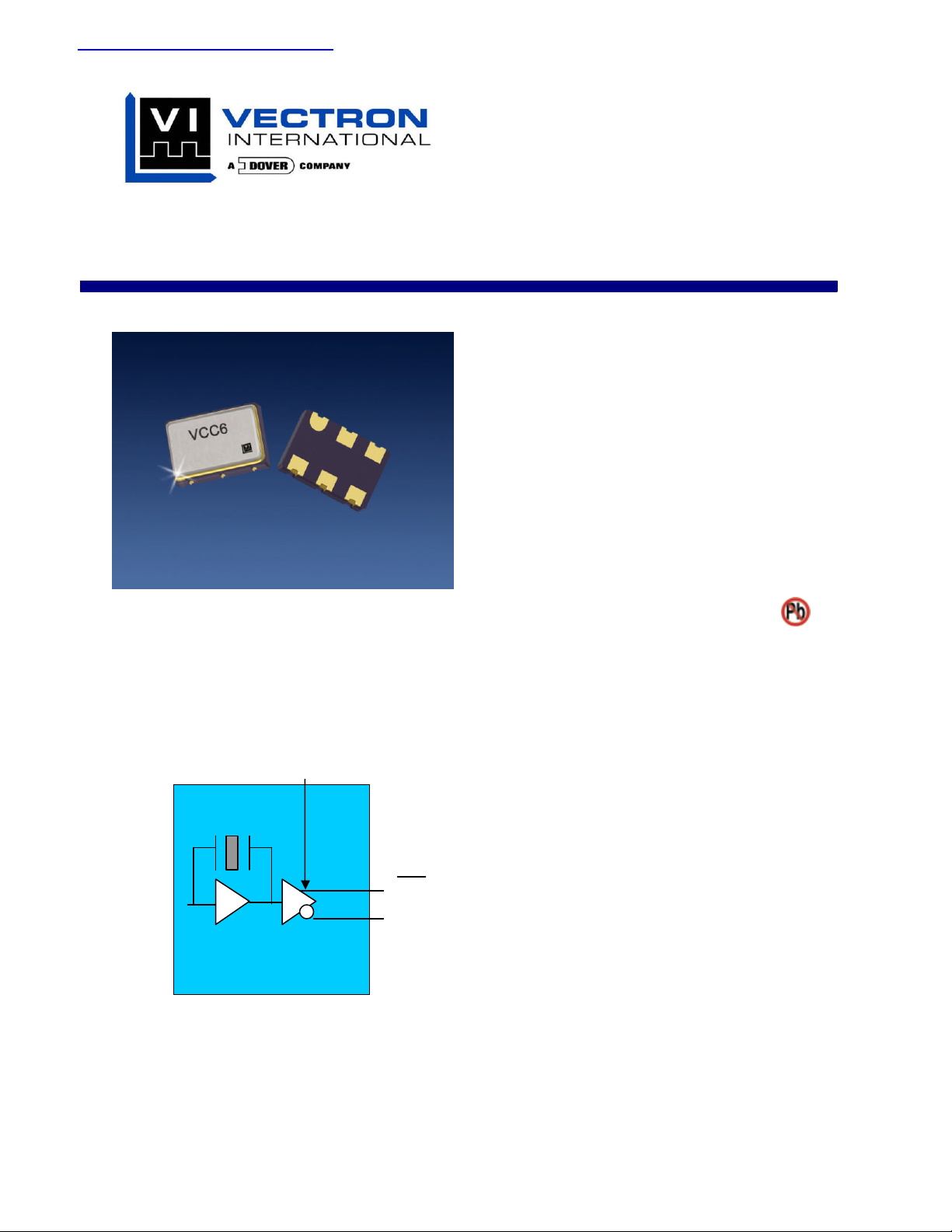
The VCC6 Crystal Oscillator
Output
Buffer /
• Hermetically sealed ceramic SMD package
• Product is compliant to RoHS directive
Applications
• SONET/SDH/DWDM
• Fiber Channel
• Ethernet, Gigabit Ethernet
• Storage Area Network
• Digital Video
• Broadband Access
Description
Vectron’s VCC6 Crystal Oscillator (XO) is quartz
stabilized square wave generator with a LV-PECL
output, operating off a 3.3 volt supply.
The VCC6 uses 3rd overtone crystals for
frequencies under 200MHz, resulting in low jitter
performance, typically 0. 3pS rms in the 12 kHz to
20MHz band.
Vectron International 267 Lowell Road, Hudson NH 03051 Tel: 1-88-VECTRON-1 e-mail: vectron@vectron.com
Page 2
VCC6-Q/R Series, 2.5 and 3.3v PECL Crystal Oscillator
tFt
Performance Characteristics
Table 1. Electrical Performance
Parameter Symbol
Frequency fO 10 270 MHz
Supply Voltage1, 3.3V Q option
VDD 3.15
2.5V R option
Supply Current IDD 98 mA
Output Logic Levels, 0/70°C
Output Logic High2
Output Logic Low2
Output Logic Levels, -40/85°C
Output Logic High2
Output Logic Low2
Transition Times
Rise Time2
Fall Time2
VOH
VOL
VOH
VOL
tR
tF
Symmetry or Duty Cycle3 SYM 45 50 55 %
Operating temperature (ordering option) TOP -10/70 or –40/85 °C
Stability (ordering option)4 deltaF/F
Jitter, 12kHz to 20MHz5
Cycle to Cycle, rms
Cycle to Cy cle, peak-peak
Period Jitter, rms
Period Jitter, peak -peak
Output Enabled6 VIH 0.7*VDD V
Output Disabled6 VIL 0.3*VDD V
Output Enable/Disable time t
200 nS
E/D
Enable/Disable Leakage Current IIL ±200 uA
Output Enable Pull-Up Resistor6
Output Enabled
Output Disabled
1. A 0.01uF and a 0.1uF capacitor should be located as close to the supply as possible and terminated to ground.
2. Figure 1 defines these parameters. Figure 2 illustrates the operating conditions under which these parameters are tested and specified.
3. Symmetry is measured defined as On Time/Period.
4. Includes calibration tolerance, operating temperature, supply voltage variations, aging (40 degreesC/10 years) and shock and vibration (not under
operation).
5. Measurements made on a VCC6-QAB-155M520 using an Agilent E5052A for phase noise and LeCroy 8600, 25K samples for jitter.
6. Output will be enabled if Enable/Disable is left open. The pull resistor changes to a higher value, operating in a “power saving mode” when
Enable/Disable is set to a logic 0.
Min Typical Maximum Units
2.375
VDD-1.025
VDD-1.810
VDD-1.085
VDD-1.830
3.3
2.5
3.45
2.625
VDD-0.880
VDD-1.620
VDD-0.880
VDD-1.555
600
600
±25, ±50 or ±100 ppm
0.3
0.7 pS
4.8
38
2.7
23
33
1
V
V
V
V
V
ps
ps
Kohm
Mohm
R
%
80
Vs
20%
On Time
Period
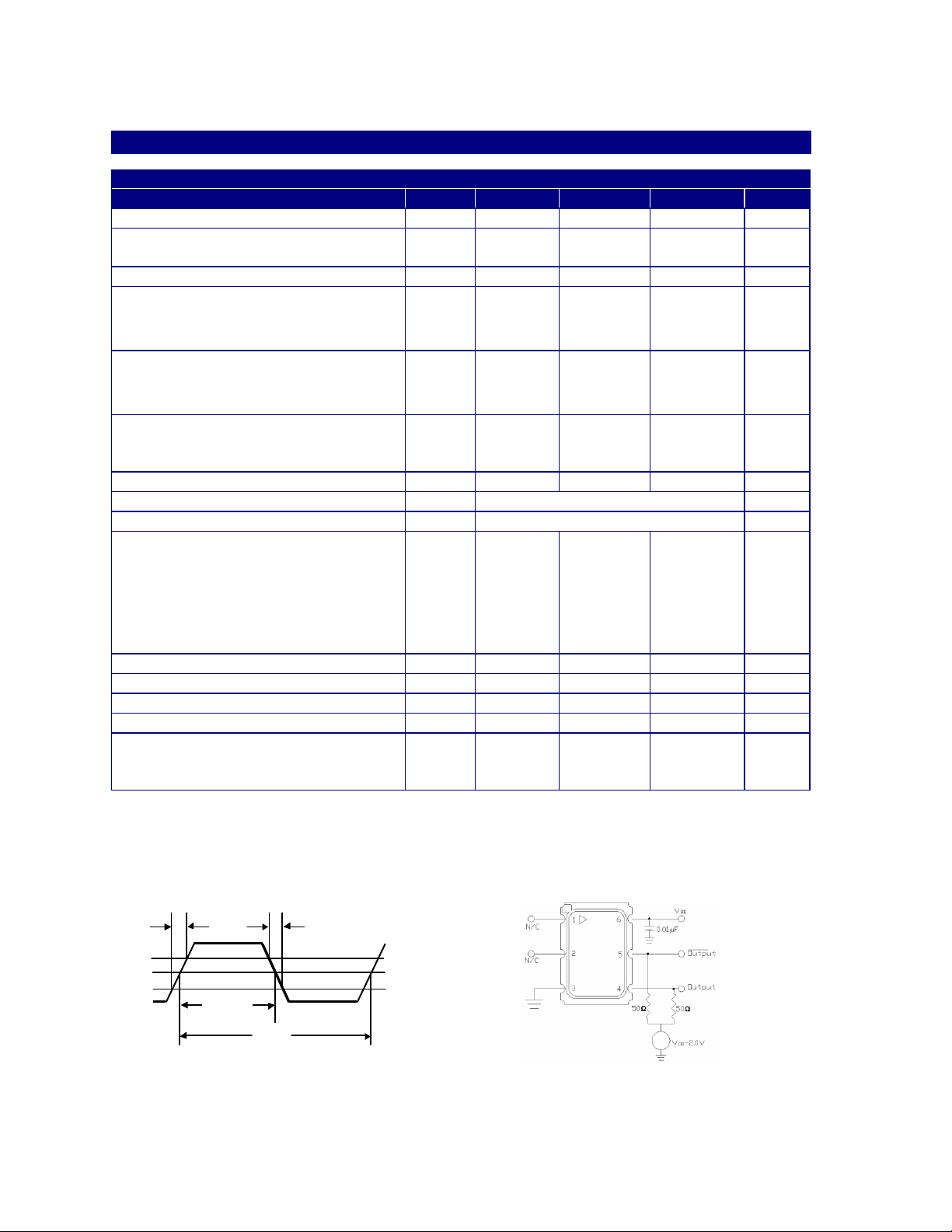
Figure 1. Output Waveform Figure 2. Typical Output Test Conditions (25±5°C)
Vectron International 267 Lowell Rd, Hudson NH 03051 Tel: 1-88-VECTRON-1 e-mail: vectron@vectron.com
Page 3
VCC6-Q/R Series, 2.5 and 3.3v PECL Crystal Oscillator
Outline Diagram and Pin Out
Table 2. VCC6-QAx Pinout
Pin # Symbol Function
1 NC This pin has no internal connection and is floating.
2 E/D Enable/Disable Function
3 GND Ground
4 fO Output Frequency
5 Cfo Complementary Output Frequency
6 VDD Supply Voltage
Gold over Nickel plating
Figure 3 Optional VCC6-QAx Package Drawing
Table 3. VCC6-QCx Pinout
Pin # Symbol Function
1 E/D Enable/Disable Function
2 NC This pin has no internal connection and is floating.
3 GND Ground
4 fO Output Frequency
5 Cfo Complementary Output Frequency
6 VDD Supply Voltage
Gold over Nickel plating
Figure 4. VCC6-QCx and VCC6-QAx Package Drawing
Vectron International 267 Lowell Rd, Hudson NH 03051 Tel: 1-88-VECTRON-1 e-mail: vectron@vectron.com
Page 4

VCC6-Q/R Series, 2.5 and 3.3v PECL Crystal Oscillator
Terminating PECL Outputs
The VCC6 incorporates a standard PECL output scheme, which are un-terminated emitters as shown in
Figure 5. There are numerous application notes on terminating and interfacing PECL logic and the two most
common methods are a single resistor to ground, Figure 6, and a pull-up/pull-down scheme as shown in
Figure 7. An AC coupling capacitor is optional, depending on the application and the input logic
requirements of the next stage.
One of the most important considerations is terminating the Output and Complementary Outputs equally.
An unused output should not be left un-terminated, and if it one of the two outputs is left open it will result in
excessive jitter on both. PC board layout must take this and 50 ohm impedance matching into account.
Load matching and power supply noise are the main contributors to jitter related problems.
Figure 5. Standard PECL Output Configuration
Figure 6. Single Resistor Termination Figure 7. Pull-up Pull-down Termination
Resistor value are typically: Resistor values are typically:
120 to 240ohms for 3.3V 130 and 82 ohms for 3.3V
82 to 120 ohms for 2.5V 240 and 62 ohms for 2.5V
Vectron International 267 Lowell Rd, Hudson NH 03051 Tel: 1-88-VECTRON-1 e-mail: vectron@vectron.com
Page 5

VCC6-Q/R Series, 2.5 and 3.3v PECL Crystal Oscillator
Enable/Disable Functional Description
Under normal operation the Enable/Disable is left open, or set to a logic high state, and the VCC6 is in
oscillation mode and outputs are enabled (active). When the E/D is set to a logic low, the oscillator stops
and the both the output and complementary outputs are in a high impedance state. This helps facilitate
board testing and troubleshooting.
Power Saving Pull-Up Resistor
The E/D pull-up resistor changes in response to the input logic level; the pull-up resistor is a large value
when E/D is set to a logic low, which reduces the current consumed. When E/D is open, or set to a logic
high, the pull-up resistance becomes a smaller value which helps decrease the effects of external noise.
Absolute Maximum Ratings
Stresses in excess of the absolute maximum ratings can permanently damage the device. Functional
operation is not implied at these or any other conditions in excess of conditions represented in the
operational sections of this data sheet. Exposure to absolute maximum ratings for extended periods may
adversely affect device reliability.
Table 4. Absolute Maximum Ratings
Parameter Symbol Ratings Unit
Power Supply VDD -0.5 to +7.0 Vdc
Enable/Disable VIN -0.5 to VDD+0.5 Vdc
Storage Temperature Tstorage -55/125 °C
Reliability
The VCC6 qualification tests included:
Table 5. Environnemental Compliance
Parameter Conditions
Mechanical Shock MIL-STD-883 Method 2002
Mechanical Vibration MIL-STD-883 Method 2007
Solderability MIL-STD-883 Method 2003
Gross and Fine Leak MIL-STD-883 Method 1014
Resistance to Solvents MIL-STD-883 Method 2016
Handling Precautions
Although ESD protection circuitry has been designed into the the VCC6, proper precautions should be taken
when handling and mounting. VI employs a Human Body Model and a Charged-Device Model (CDM) for
ESD susceptibility testing and design protection evaluation. ESD thresholds are dependent on the circuit
parameters used to define the model. Although no industry wide standard has been adopted for the CDM, a
standard HBM of resistance = 1.5kohms and capacitance = 100pF is widely used and therefore can be
used for comparison purposes.
Table 6. ESD Ratings
Model Minimum Conditions
Human Body Model 1500 MIL-STD-883 Method 3015
Charged Device Model 1000
Vectron International 267 Lowell Rd, Hudson NH 03051 Tel: 1-88-VECTRON-1 e-mail: vectron@vectron.com
Page 6
VCC6-Q/R Series, 2.5 and 3.3v PECL Crystal Oscillator
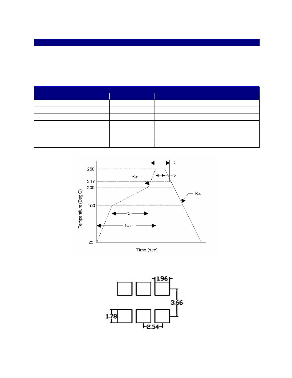
IR Reflow and Suggested Pad Size Layout
The VCC6 has been qualified to meet the JEDEC standard for Pb-Free assembly. The temperatures and
time intervals listed are based on the Pb-Free small body requirements and maximum parameters are listed
in Table 6, lower temperatures are also acceptable. The VCC6 is hermetically sealed so an aqueous wash
is not an issue. Frequencies >200MHz will need to be reflowed at 220C max.
Table 7. Reflow Profile (IPC/JEDEC J-STD-020B)
Parameter Symbol Value
PreHeat Time
Ramp Up
t S 60 sec Min, 200 sec Max
R
3 oC/sec Max
UP
Time Above 217 oC t L 60 sec Min, 150 sec Max
Time To Peak Temperature
Time At 260 oC (max)
Time At 240°C (max)
Ramp Down
t
480 sec Max
AMB -P
t P 10 sec Max
tp2 60 sec MAX
R
6 oC/sec Max
DN
Figure 8. IR Reflow Diagram
Figure 9. Pad Size Diagram
Vectron International 267 Lowell Rd, Hudson NH 03051 Tel: 1-88-VECTRON-1 e-mail: vectron@vectron.com
Page 7

VCC6-Q/R Series, 2.5 and 3.3v PECL Crystal Oscillator
Tape and Reel
J
F
CD
A
G
B
L
I
E
KH
Figure 10. Tape and Reel Diagram
Table 8. Tape and Reel Dimensions (mm)
Tape Dimensions Reel Dimensions # Per
Product A B C D E F G H I J K L Reel
VCC6
16 7.5 1.5 4 8 2 21 13 60 2 17 180
250
Vectron International 267 Lowell Rd, Hudson NH 03051 Tel: 1-88-VECTRON-1 e-mail: vectron@vectron.com
Page 8
VCC6-Q/R Series, 2.5 and 3.3v PECL Crystal Oscillator
)
Table 9. Standard Frequencies (MHz)
19.440 27.000 27.027 35.000 37.000 38.880
40.000 40.680 48.000 50.000 52.300 62.500
64.000 64.375 74.1758 74.250 76.800 77.760
80.000 83.125 87.000 90.000 91.875 93.000
98.304 100.000 105.000 106.000 106.250 110.000
125.000 130.000 130.5882 133.000 134.560729 135.000
136.000 143.000 145.221 150.000 153.500 155.520
156.000 156.250 156.256 156.260 159.375 160.000
160.160 161.1328 163.235 164.3555 165.000 166.000
166.6286 166.6667 166.67 167.00 167.3316 168.200912
171.000 173.3707 175.000 180.000 187.500 190.000
195.3125 200.000 212.500 250.000 260.000
Other frequencies may be available upon request. Standard frequencies are frequencies which the crystal
has been designed and does not imply a stock position.
Ordering Information
VCC6 – Qxx – xxxMxx
Product Family Frequency MHz
Crystal Oscillator example: 125M00= 125.000
Supply Voltage, Output Stability Options/Temperature
Q=3.3V, LVPECL A: ±100ppm -10 to 70°C
R=2.5V, LVPECL B: ±50ppm -10 to 70°C
Enable/Disable C: ±100ppm -40 to 85°C
A: E/D is on Pin 2, Pin 1 is a NC D: ±50ppm -40 to 85°C
C: E/D is on Pin 1, Pin 2 is a NC E: ±25ppm -10 to 70°C
F: ±25ppm -40 to 85°C
NOTE: Not all combinations of options are available.
A ±20ppm option over -10/70°C 3.3V, VCC6-107-frequency, is also available
A ±20ppm option over -10/70°C 2.5V, VCC6-110-frequency, is also available.
www.vectron.com
Vectron International reserves the right to make changes to the product(s) and/or information contained herein without notice. No liability is assumed
as a result of their use or application. No rights under any patent accompany the sale of any such product(s) or information.
VCC6-Q/R (REVISION DATE: September 07, 2005
For Additional Information, Please Contact:
USA: Vectron International • 267 Lowell Road, Hudson, NH 03051
• Tel: 1-88-VECTRON-1 • Fax: 1-888-FAX-VECTRON
EUROPE: Landstrasse, D-74924, Neckarbischofsheim, Germany •
Tel: 49 (0) 7268 8010 • Fax: 49 (0) 7268 801281
ASIA: Vectron Asia Pacific Sales 1F~2F. No.8 Workshop No.308 Fenju Rd., WaiGaoQiao Free
Trade Zone, Pudong New Area Shanghai, China 200131
•Tel: 8621 50480777 • Fax: 8621 50481881
Vectron International 267 Lowell Rd, Hudson NH 03051 Tel: 1-88-VECTRON-1 e-mail: vectron@vectron.com
Page 9

Copyright © Each Manufacturing Company.
All Datasheets cannot be modified without permission.
This datasheet has been download from :
www.AllDataSheet.com
100% Free DataSheet Search Site.
Free Download.
No Register.
Fast Search System.
www.AllDataSheet.com
 Loading...