

查询VCC1-G0A-125M00供应商
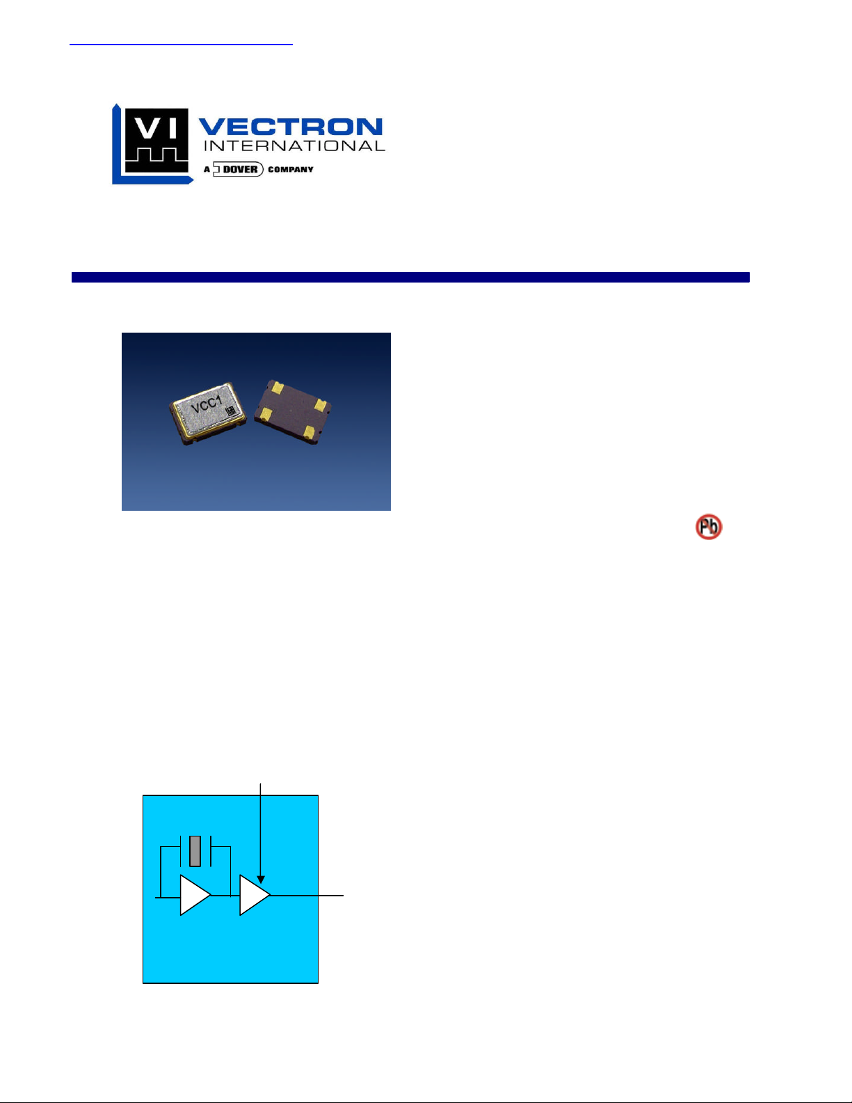
VCC1 series
1.8, 2.5, 3.3, 5.0 volt CMOS Oscillator
Features
• CMOS output
• Output frequencies to 190 MHz
• Low jitter, Fundamental or 3rd OT Crystal
• Tristate output for board test and debug
• -10/70 or –40/85 °C operating temperature
• Gold over nickel contact pads
• Hermetically sealed ceramic SMD package
The VCC1 Crystal Oscillator
Output
Buffer /
Disable
• Product is compliant to RoHS directive
and fully compatible with lead free assembly
Applications
• SONET/SDH/DWDM
• Ethernet, Gigabit Ethernet
• Storage Area Network
• Digital Video
• Broadband Access
• Microprocessors/DSP/FPGA
Description
Vectron’s VCC1 Crystal Oscillator (XO) is quartz
stabilized square wave generator with a CMOS
output, operating off either a 1.8, 2.5, 3.3 or a 5.0
volt supply.
f
o
The VCC1 is uses fundamental or 3rd overtone
crystals resulting in low jitter performance,
typically 0.5pS rms in the 12 kHz to 20MHz
band. Also a monolithic IC, which improves
reliability and reduces cost, is hermitically
sealed.
Vectron International 267 Lowell Road, Hudson NH 03051 Tel: 1-88-VECTRON-1 e-mail: vectron@vectron.com
+
+
-
3
2
4 1
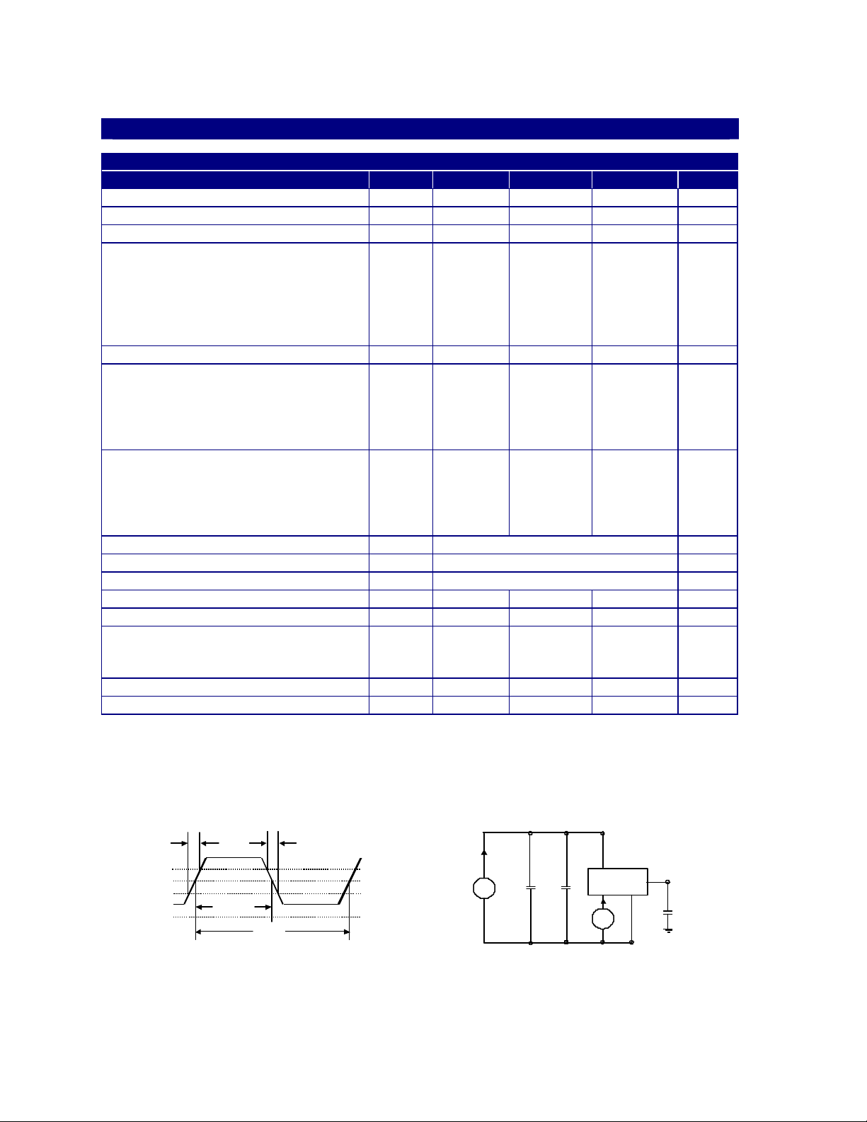
Performance Characteristics
Table 1. Electrical Performance , 5V option
Parameter Symbol
Frequency fO 0.012 125.000 MHz
Operating Supply Voltage 1 VDD 4.5 5.5 V
Absolute Maximum Supply Voltage -0.7 7.0 V
Supply Current , Output Enabled
IDD
<1.5 MHz
1.5 to 20 MHz
20.01 to 50 MHz
50.00 to 85 MHz
85.01 to 125 MHz
Supply Current, Out disabled IDD 30 uA
Output Logic Levels
Output Logic High2
Output Logic Low
2
Output Logic High Drive
Output Logic Low Drive
Output Rise/Fall Time2
VOH
V
OL
I
OH
IOL
tR/tF
< 1.00 MHz
1.0 to 20.00 MHz
20.01 to 50.00 MHz
50.01 to 125.00 MHz
Duty Cycle3 (ordering option) SYM 45/55 %
Operating temperature (ordering option) -10/70 or -40/85 °C
Stability4 (ordering option) ±20, ±25, ±32, ±50, ±100 ppm
RMS Jitter, 12kHz to 20 MHz 0.5 1 ps
Period Jitter, RMS 2.5 ps
Output Enable/Disable
5
Output Enabled
Output Disabled
Internal Enable Pull-Up resistor5 100 Kohm
Start-up time 10 ms
1. A 0.01uF and a 0.1uF capacitor should be located as close to the supply as possible (to ground) is recommended.
2. Figure 1 defines these parameters. Figure 2 illustrates the operating conditions under which these parameters are tested and
specified.
3. Symmetry is measured defined as Vs, On Time/Period.
4. Includes calibration tolerance, operating temperature, supply voltage variations, aging and shock and vibration (not under
operation).
5. Output will be enabled if enable/disable is left open.
R
V
OH
50%
V
OL
On Time
Period
tFt
Figure 1. Output Waveform Figure 2. Typical Output Test Conditions (25±5°C)
Min Typical Maximum Units
7
10
30
50
60
0.9*VDD
0.1*VDD
16
16
200
8
5
2
4.0
0.8
I
DD
V
.1µF
DD
.01µF
IC
V
C
15pF
-
mA
V
V
mA
mA
ns
V
Vectron International 267 Lowell Rd, Hudson NH 03051 Tel: 1-88-VECTRON-1 e-mail: vectron@vectron.com
VCC1 Data sheet
+
+
-
3
2
4 1
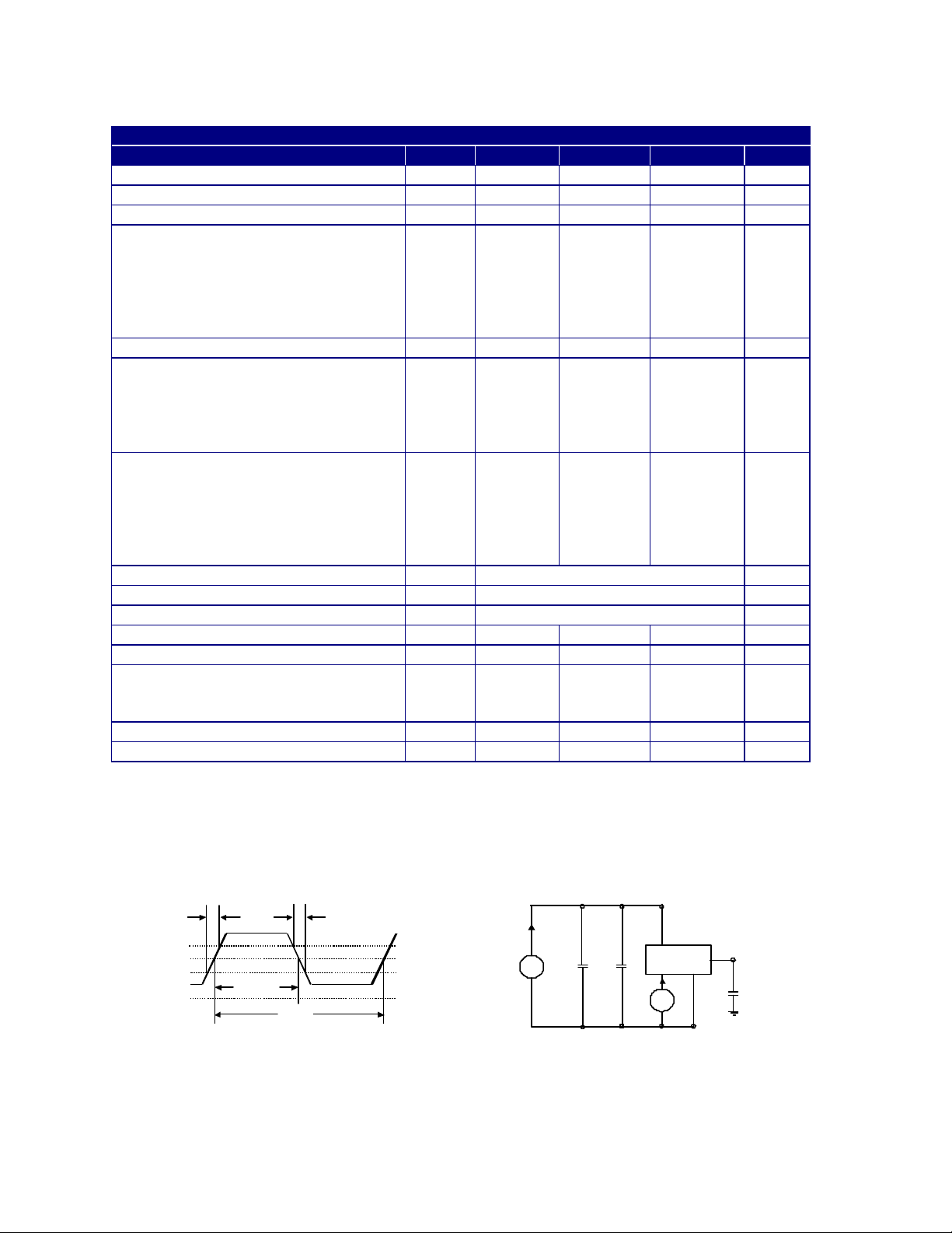
Table 2. Electrical Performance, 3.3V option
Parameter Symbol
Frequency fO 0.012 189.000 MHz
Operating Supply Voltage 1 VDD 2.97 3.3 3.63 V
Absolute Maximum Operating Voltage -0.5 5.0 V
Supply Current, Output Enabled
IDD
< 1.500 MHz
1.5 to 20 MHz
20.01 to 50 MHz
50.00 to 85 MHz
85.01 to 189 MHz
Supply Current, Out put disabled IDD 30 uA
Output Logic Levels
Output Logic High2
Output Logic Low
2
Output Logic High Drive
Output Logic Low Drive
Output Rise/Fall Time2
VOH
V
OL
I
OH
IOL
tR/tF
< 1.00 MHz
1.00 to 20.00 MHz
20.01 to 50.00 MHz
50.01 to 90.00 MHz
90.01 to 189.00 MHz
Duty Cycle3 (ordering option) SYM 45/55 %
Operating temperature (ordering option) -10/70 or –40/85 °C
Stability4 (ordering option) ±20, ±25, ±32, ±50, ±100 ppm
RMS Jitter, 12kHz to 20 MHz 0.5 1 ps
RMS Jitter 2.5 ps
Output Enable/Disable
5
Output Enabled
Output Disabled
Internal Enable Pull-Up resistor5 100 Kohm
Start-up time 10 ms
1. A 0.01uF and a 0.1uF capacitor should be located as close to the supply as possible (to ground) is recommended.
2. Figure 3 defines these parameters. Figure 4 illustrates the operating conditions under which these parameters are tested and
specified. For Fo>90MHz, rise and fall time is measured 20 to 80%.
3. Symmetry is measured defined as Vs, On Time/Period.
4. Includes calibration tolerance, operating temperature, supply voltage variations, aging and shock and vibration (not under
operation).
5. Output will be enabled if enable/disable is left open.
R
V
OH
50%
V
OL
On Time
Period
tFt
Figure 3. Output Waveform Figure 4. Typical Output Test Conditions (25±5°C)
Min Typical Maximum Units
5
7
20
30
50
0.9*VDD
0.1*VDD
8
8
200
6
4
3
2
2.0
0.5
I
DD
V
.1µF
DD
.01µF
IC
V
C
15pF
-
mA
V
V
mA
mA
ns
V
Vectron International 267 Lowell Rd, Hudson NH 03051 Tel: 1-88-VECTRON-1 e-mail: vectron@vectron.com

VCC1 Data sheet
-
3
tFt
Table 3. Electrical Performance, 2.5V option
Parameter Symbol
Frequency fO 0.012 172.000 MHz
Operating Supply Voltage 1 VDD 2.25 2.5 2.75 V
Absolute Maximum Voltage -0.5 5.0 V
Supply Current, Output Enabled
IDD
< 20 MHz
20.01 to 50 MHz
50.00 to 110 MHz
110.1 to 172 MHz
Supply Current, Out disabled IDD 30 uA
Output Logic Levels
Output Logic High2
Output Logic Low
2
Output Logic High Drive
Output Logic Low Drive
Output Logic High Drive
Output Logic Low Drive3
Output Rise/Fall Time2
3
VOH
V
OL
I
OH
IOL
I
OH
IOL
tR/tF
<1.00 MHz
1.00 to 20.00 MHz
20.01 to 50.00 MHz
50.01 to 90.00 MHz
90.01 to 172.00 MHz
Duty Cycle4 (ordering option) SYM 45/55 %
Operating temperature (ordering option) -10/70 or –40/85 °C
Stability5 (ordering option) ±20, ±25, ±32, ±50, ±100 ppm
RMS Jitter, 12kHz to 20 MHz 0.5 1 ps
RMS Jitter 2.5 ps
Output Enable/Disable
6
Output Enabled
Output Disabled
Internal Enable Pull-Up resistor6 100 Kohm
Start-up time 10 ms
1. A 0.01uF and a 0.1uF capacitor should be located as close to the supply as possible (to ground) is recommended.
2. Figure 5 defines these parameters. Figure 6 illustrates the operating conditions under which these parameters are tested and
specified.
3. Overtone designs, output frequencies>35MHz.
4. Symmetry is measured defined as Vs, On Time/Period.
5. Includes calibration tolerance, operating temperature, supply voltage variations, aging and shock and vibration (not under
operation).
6. Output will be enabled if enable/disable is left open.
R
%
80
Vs
20%
On Time
Period
Figure 5. Output Waveform Figure 6. Typical Output Test Conditions (25±5°C)
Min Typical Maximum Units
7.0
15.0
20.0
30.0
0.9*VDD
0.1*VDD
4
4
8
8
200
10
6
3
2
1.75
0.5
I
DD
+
.1µF
V
DD
.01µF
4
2
1
IC
15pF
+
VC
-
mA
V
V
mA
mA
mA
mA
ns
V
Vectron International 267 Lowell Rd, Hudson NH 03051 Tel: 1-88-VECTRON-1 e-mail: vectron@vectron.com

VCC1 Data sheet
tFt
-
3
Table 4. Electrical Performance, 1.8V option
Parameter Symbol
Frequency fO 0.048 172.000 MHz
Operating Supply Voltage 1 VDD 1.71 1.8 1.89 V
Absolute Maximum Voltage -0.5 3.6 V
Supply Current, Output Enabled
IDD
< 20 MHz
20.01 to 70 MHz
70.01 to 96 MHz
96.01 to 125 MHz
125.01 to 172 MHz
Supply Current, Out disabled IDD 30 uA
Output Logic Levels
Output Logic High2
Output Logic Low
2
Output Logic High Drive
Output Logic Low Drive
Output Logic High Drive3
Output Logic Low Drive3
Output Rise/Fall Time
2
VOH
V
OL
I
OH
IOL
I
OH
IOL
tR/tF
< 1.00 MHz
1.000 to 20.00 MHz
20.01 to 50.00 MHz
50.00 to 90.00 MHz
90.01 to 172.00 MHz
Duty Cycle4 (ordering option) SYM 45/55 %
Operating temperature (ordering option) -10/70 or –40/85 °C
Stability5 (ordering option) ±20, ±25, ±32, ±50, ±100 ppm
RMS Jitter, 12kHz to 20 MHz 0.5 ps
RMS Jitter 2.2 ps
Output Enable/Disable
6
Output Enabled
Output Disabled
Internal Enable Pull-Up resistor6 1 Mohm
Start-up time 10 ms
1. A 0.01uF and a 0.1uF capacitor should be located as close to the supply as possible (to ground) is recommended.
2. Figure 7 defines these parameters. Figure 8 illustrates the operating conditions under which these parameters are tested and
specified.
3. Overtone designs, output frequencies>35MHz.
4. Symmetry is measured defined as Vs, On Time/Period.
5. Includes calibration tolerance, operating temperature, supply voltage variations, aging and shock and vibration (not under
operation).
6. Output will be enabled if enable/disable is left open.
R
%
80
Vs
20%
On Time
Period
Figure 7. Output Waveform Figure 8. Typical Output Test Conditions (25±5°C)
Min Typical Maximum Units
5
15
20
25
30
0.9*VDD
0.1*VDD
2.8
2.8
8
8
200
4
4
3
2
1.26
0.5
I
DD
+
.1µF
V
DD
.01µF
4
2
1
IC
15pF
+
VC
-
mA
V
V
mA
mA
mA
mA
ns
V
Vectron International 267 Lowell Rd, Hudson NH 03051 Tel: 1-88-VECTRON-1 e-mail: vectron@vectron.com

VCC1 Data sheet
Enable/Disable Functional Description
Under normal operation the Enable/Disable is left open or set to a logic high state. When the E/D is set to a
logic low, the oscillator stops and the output is in a high impedance state. This helps reduce power
consumption as well as facilitating board testing and troubleshooting.
TriState Functional Description
Under normal operation the Tristate is left open or set to a logic high state. When the Tri-State is set to a
logic low, the oscillator remains active but the output buffer is in a high impedance state. This helps facilitate
board testing and troubleshooting.
Outline Diagrams, Pad Layout and Pin Out
Pin # Symbol Function
1 E/D or NC Tristate, Enable/Disable or NC
2 GND Electrical and Case Ground
3 fO Output Frequency
4 VDD Supply Voltage
Contact Pads are gold over nickel
Figure 9, Packa ge drawing
Vectron International 267 Lowell Rd, Hudson NH 03051 Tel: 1-88-VECTRON-1 e-mail: vectron@vectron.com

VCC1 Data sheet
Contact Pads are gold over nickel
Figure 10, Alternate Package drawing
Tape and Reel
Table 5: Tape and Reel Dimensions (mm)
J
F
CD
A
E
G
B
I
L
KH
Tape Dimensions Reel Dimensions # Per
Product A B C D E F G H I J K L Reel
VCC1
12 5.5 1.5 4 8 1.78 20.6 13 55 6 12.4 178
1000
Vectron International 267 Lowell Rd, Hudson NH 03051 Tel: 1-88-VECTRON-1 e-mail: vectron@vectron.com

VCC1 Data sheet
Absolute Maximum Ratings
Stresses in excess of the absolute maximum ratings can permanently damage the device. Functional
operation is not implied at these or any other conditions in excess of conditions represented in the
operational sections of this data sheet. Exposure to absolute maximum ratings for extended periods may
adversely affect device reliability.
Table 6. Absolute Maximum Ratings
Parameter Symbol Ratings Unit
Storage Temperature Tstorage -55/125 °C
Reliability
The VCC1 qualification tests have included:
Table 7. Environnemental Compliance
Parameter Conditions
Mechanical Shock MIL-STD-883 Method 2022
Mechanical Vibration MIL-STD-883 Method 2007
Temperature Cycle MIL-STD-883 Method 1010
Solderability MIL-STD-883 Method 2003
Gross and Fine Leak MIL-STD-883 Method 1014
Resistance to Solvents MIL-STD-883 Method 2015
Handling Precautions
Although ESD protection circuitry has been designed into the the VCC1, proper precautions should be taken
when handling and mounting. VI employs a Human Body Model and a Charged-Device Model (CDM) for
ESD susceptibility testing and design protection evaluation. ESD thresholds are dependent on the circuit
parameters used to define the model. Although no industry wide standard has been adopted for the CDM, a
standard HBM of resistance = 1.5kohms and capacitance = 100pF is widely used and therefore can be
used for comparison purposes.
Table 8. ESD Ratings
Model Minimum Conditions
Human Body Model 1000 MIL-STD-883 Method 3115
Charged Device Model 1500 JESD 22-C101
Vectron International 267 Lowell Rd, Hudson NH 03051 Tel: 1-88-VECTRON-1 e-mail: vectron@vectron.com

VCC1 Data Sheet
Suggested IR profile
Devices are built using lead free epoxy and can also be subjected to standard lead free IR reflow conditions,
Table 9 shows max temperatures and lower temperatures can also be used e.g. peak temperature of 220C.
Table 9. Reflow Profile (IPC/JEDEC J-STD-020B)
Parameter Symbol Value
PreHeat Time
Ramp Up
t S 150 sec Min, 200 sec Max
R
3 oC/sec Max
UP
Time Above 217 oC t L 60 sec Min, 150 sec Max
Time To Peak Temperature
Time At 260 oC (max)
Time At 240 °C (max)
Ramp Down
t
480 sec Max
AMB -P
t P 10 sec Max
tp2 60 sec Max
R
6 oC/sec Max
DN
Vectron International 267 Lowell Rd, Hudson NH 03051 Tel: 1-88-VECTRON-1 e-mail vectron@vectron.com
9

VCC1 Data Sheet
B3 B 125M00
Ordering Information
VCC1 - -
Product Family Output Frequency
Crystal Oscillator In MHZ
Voltage Options
A: +5.0 Vdc +/-10% , 15pF
B: +3.3 Vdc +/-10%, 15pF
C: +3.0 Vdc +/-10%, 15pF
E: +5.0 Vdc +/-10%, 50pF
F: +3.3Vdc +/-10%, 50pF
G: +2.5Vdc +/-10%, 15pF
H: +1.8Vdc +/-10%, 15pF
Note: Not all combinations are available. Tristate with a 45/55% is the most common Electrical code and is
recommended for most applications.
Electrical Options
3: Tristate, 45/55% Duty
The following codes are not
recommended for new designs
0: No tristate, 40/60% Duty
1: Tristate, 40/60% Duty
2: No tristate, 45/55%Duty
5: Enable, 40/60% Duty
6: Enable, 45/55% Duty
For Additional Information, Please Contact:
Stability Options
A: ±100ppm, -10 to 70C
C: ±100ppm, -40 to 85C
B: ±50ppm, -10 to 70C
D: ±50ppm, -40 to 85C
K: ±32ppm, -10 to 70C
O: ±32ppm, -40 to 85C
E: ±25ppm, -10 to 70C
F: ±25ppm, -40 to 85C
G: ±20ppm, -10 to 70C
USA: Vectron International • 267 Lowell Road, Hudson, NH 03051
• Tel: 1-88-VECTRON-1 • Fax: 1-888-FAX-VECTRON
EUROPE: VI Telefilter · Potsdamer Straße 18, 14513 Teltow, Germany
Tel: 49 (0) 3328 4784 17 · Fax: 49 (0) 3328 4784 30
www.vectron.com
April 19, 2005
Vectron International 267 Lowell Rd, Hudson NH 03051 Tel: 1-88-VECTRON-1 e-mail vectron@vectron.com
ASIA: Vectron Asia Pacific Sales Office Unit 3119 31st Floor, Jin Mao Tower,
88 Century Boulevard, Shanghai, P.R. China 200120
Tel: +86 21 28909740 / 41 / 42 · Fax: +86 21 28909240 / 2890999
10
 Loading...