

Page 1
iI=torn =tArn
U)E=i) mAnUAL .
Page 2

Page 3
PROM!RAM III BOARD
Revision 1
PROM PROGRAMMING PROGRAM
Revision 1
USERS MANUAL
Revision A"
July 16, 1979
Page 4
Copyright 1979 by Vector Graphic Inc.
All rights reserved.
Disclaimer
Vector Graphic makes no representations or warranties with respect to the
contents of this manual itself, even if the product it describes is covered
by a warranty or repair agreement. Further, Vector Graphic reserves the
right to revise this publication and to make changes from time to time in
the content hereof without obligation of Vector Graphic to notify any person
of such revision or changes, except when an agreement to the contrary
exists.
Revision Numbers
The date and revision of each page herein appears at the bottom of each
page. The revision letter such as A or B changes if the manual has been
improved but the product itself has not been significantly modified. The
da~e and revision on the Title Page corresponds to that of the page most
.recently revised. When the product itself is modified significantly, the
product will get a new revision number, as shown on the manual's title page,
and the manual will revert to revision A, as if it were treating a brand new
product. THIS MANUAL SHOULD ONLY BE USED WITH THE PRODUCT(S) IDENTIFIED ON
THE TITLE PAGE.
(-/'
""-"--~
.
Page 5
The PROM RAM III Board sold hereunder is sold "as is", with all faults and
without any warranty, either expressed or implied, including any implied
warranty of fitness for intended use or merchantability. However, the above
notwithstanding, VECTOR GRAPHIC, INC., will, for a period of ninety (90)
days following delivery to customer, repair or replace any PROM RAM III
Board that is found to contain defects in materials or workmanship,
provided:
1. Such defect in material or workmanship existed at the time the
PROM RAM III Board left the VECTOR GRAPHIC, INC., factory,
2. VECTOR GRAPHIC, INC., is given notice of the precise defect
claimed within ten (10) days after its discovery,
3. The PROM RAM III Board is promptly returned to VECTOR GRAPHIC,
INC., at customer's expense, for examination by VECTOR GRAPHIC, INC., to
confirm the alleged defect, and for subsequent repair or replacement if
found to be in order.
Repair, replacement or correction of any defects in material or workmanship
which are discovered after expiration of the period set forth above will be
performed by VECTOR GRAPHIC, INC., at Buyer's expense, provided the PROM RAM
III Board is returned, also at Buyer's expense, to VECTOR GRAPHIC, INC., for
such repair, replacement or correction. In performing any repair,
replacement or correction after expiration of the period set forth above,
Buyer will be charged in addition to the cost of parts the then-current
VECTOR GRAPHIC, INC., repair rate. At the present time the applicable rate
is $35.00 for the first hour, and $18.00 per hour for every hour of work
required thereafter. Prior to commencing any repair, replacement or
correction of defects in material or workmanship discovered after expiration
of the period for no-cost-to-Buyer repairs, VECTOR GRAPHIC, INC., will
submit to Buyer a written estimate of the expected charges, and VECTOR"·
GRAPHIC, INC., will not commence repair until such time as the written
estimate of charges has been returned by Buyer to VECTOR GRAPHIC, INC.,
signed by duly authorized representative authorizing VECTOR GRAPHIC, INC.,
to commence with the repair work involved. VECTOR GRAPHIC, INC., shall have
no obligation to repair, replace or correct any PROM RAM III Board until the
written estimate has been returned with approval to proceed, and VECTOR
GRAPHIC, INC., may at its option also require prepayment of the estimated
repair charges prior to commencing work.
Repair Agreement void if the enclosed card is not returned to VECTOR
GRAPHIC, INC. within ten (10) days of end consumer purchase.
Page 6

Page 7
Repair Agreement
Table of Contents
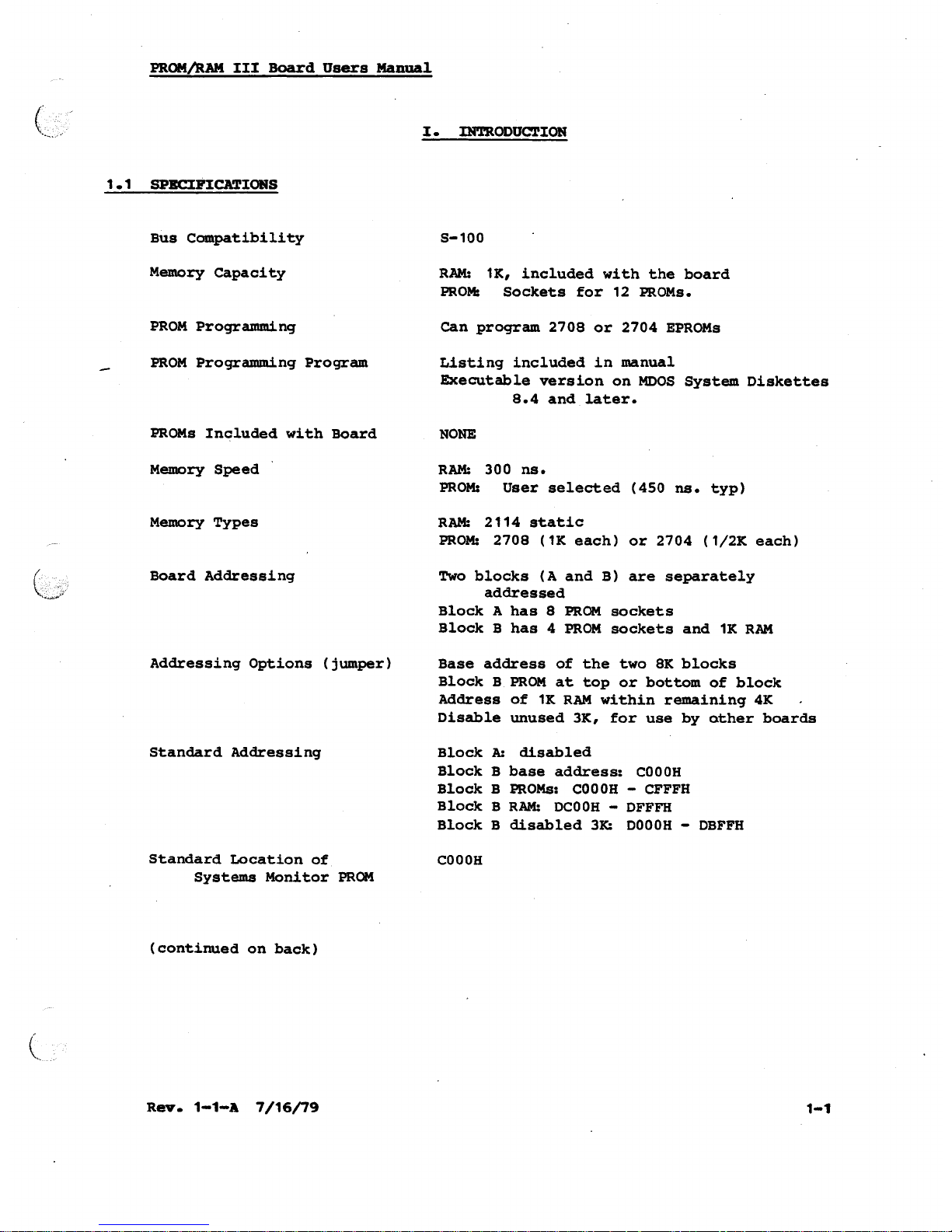
Specifications •...•••••.••.•.••••.•.••••.•••••.•..•••..•.••••. 1-1
Description of the PROM/RAM III Board ••••••••••••••••••••••••• 1-3
2.1
2.2
2.3
2.4
2.5
Block A and Block B - General ••••••••••••••••••••••••••••••••• 2-2
Block A•• ~••••••••••••••••.••••••••••••••••••••••••••••••••••• 2-3
Block B•••••••••••••••••••••••••••••••••••••••••••••••••••••••
~-3
Figures 2&3 - EXamples of Block B Configurations •••••••••••• 2-5
Block Select Addressing ••••••••••••••••••••••••••••••••••••••• 2-6
PROM/Scratchpad Memory Invert ••••••••••••••••••••••••••••••••• 2-6
RAM Memory Address Select in Block B •••••••••••••••••••••••••• 2-7
Disable 3K of Address Space in Block B •••••••••••••••••••••••• 2-7
Power-on/Reset Jump - Description ••••••••••••••••••••••••••••• 2-8
Use PRESET or POC for Power-on/Reset Jump ••••••••••••••••••••• 2-8
Phantom Generated if Power-on/Reset ••••••••••••••••••••••••••• 2-9
Jump to PROM/RAM III Board if Power-on/Reset •••••••••••••••••• 2-9
2.6
2.7
2.8
2.9
2.10
2.11
2.12
2.13
2.14
2.15
2.16
2.17
Block Swap•••••••••••••••••••••••••••••••••••••••••••••••••••• 2-1 0
Disable Power-on/Reset Response ••••••••••••••••••••••••••••••• 2-10
MWR.ITE •••••••••••••••••••••••••••••••••••••••••••••••••••••••• 2-10
Wait Sta~e Generation ••••••••••••••••••••••••••••••••••••••••• 2-11
2.18 Programming a PROM - Normal Procedure •••••••.•••••••••••••••••• 2-13
2.19 Writing a PROM Programming Program •••••••••••••••••••••••••••• 2-16
2.20 Re-assembling the PROM Programming program •••••••••••••••••••• 2-17
2.21 PROM Programming Program Listing ••••••••••••••••••••••• 2-18 - 2-24
3.1 Addressinq •••••••••••••••••.••••.••••••••••••••••••••. _••••••••• 3-1
3.2 Data Inp:ut/Output••••'•••••••••••••••••••••••••••••••••••••••••• 3-2
3.3 Control Signals •••••••••••••••....••••....•••••••
e .•••••••••••••
3-2
3.4
PR.OM
Proqramminq ••••••••••••••••••••••••••••••••••••••••••••••• 3-3
3.4 Power Supplies ••••••••••••••••••••••••••••••••••••••••••••••••• 3-4
Page 8
Board Layout ••••••••••••••••••••••••••••••••••••••••••••••••••• 4-1
Schematic Errata ••••••••••••••••••••••••••••••••••••••••••••••• 4-2
Schem.tic •••••••••••..•••.•••••••••••••••••••••••.•.•••••••••••• 4-3
Page 9
Standard Location of
Systems Monitor PROM
RAM: 1K, included with the board
PROM: Sockets for 12 PROMs.
Listing included in manual
Executable version on MOOS System Diskettes
8.4 and later.
RAM: 300 ns.
PROM: User selected (450 ns. typ)
RAM: 2114 static
PROM: 2708 (1K each) or 2704 (1/2K each)
Two blocks (A and B) are separately
addressed
Block A has 8 PROM sockets
Block B has 4 PROM sockets and 1K RAM
Base address of the two 8K blocks
Block B PROM at top or bottom of block
Address of 1K RAM within remaining 4K
Disable unused 3K, for use by other boards
Block
k
disabled
Block B base address: COOOH
Block B PROMs: COOOH - CFFFH
Block B RAM: DCOOH - DFFFH
Block B disabled 3K: DOOOH - DBFFH
Page 10
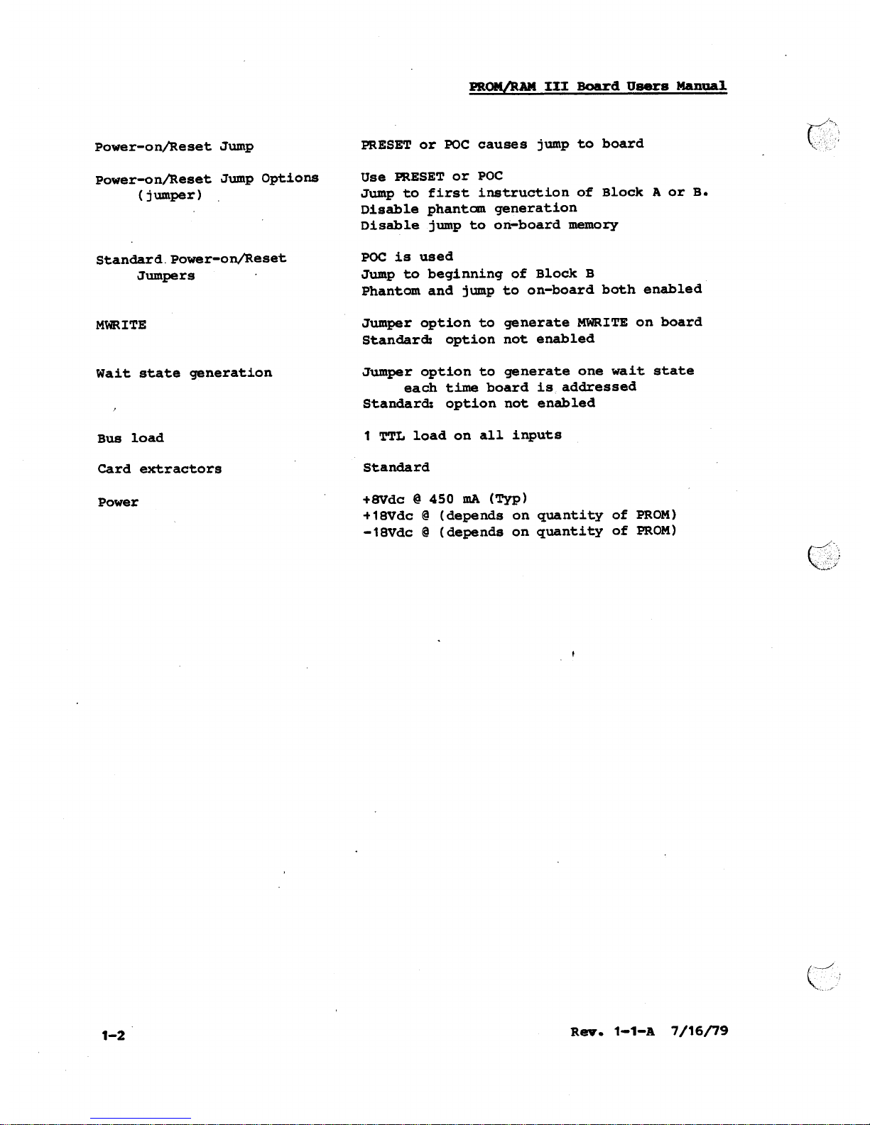
Power-on/Reset Jump Options
(jumper)
Use PRESETor POC
Jump to first instruction of Block A or
B.
Disable phantom generation
Disable jump to on-board memory
Standard.power-on/Reset
Jumpers
POCis used
Jump to beginning of Block B
Phantom and jump to on-board both enabled
Jumper option to generate MWRlTEon board
Standar~ option not enabled
Jumper option to generate one wait state
each time board is addressed
Standard: option not enabled
+8Vdc@450 mA(Typ)
+18Vdc
@
(depends on quantity of PROM)
-18Vdc
@
(depends on quantity of PROM)
(~,
~,..:>,>,
Page 11
Vector Graphic's PROMRAMIII Board is a versatile, S-100 bus compatible,
high density memoryboard combining the memory technologies of erasable
programmableread only memories (EPROMs)and high speed randomaccess memory
(RAM). Of unique value, one of the PROMsockets on the board can be used to
program a 2708 or 2704 EPROM,enabling any owner to create PROM-based
software for use on this board or in any other 1J!icroprocessor device. 1Kof
RAMis provided on the board, but no PROMsare included with purchase. The
software which is used to program PROMsis provided as a listing in this
manual, and is included on disk with all Vector Graphic systems shipped with
this board.
By
combining the use of MSIdecoding logic and unique addressing features, a
wide range of applications requirements may be met by this memoryboard.
The addressing flexibility is as follows. The board offers two
independently addressable 8Kblocks of memory(A and B). Youuse jumpers to
specify the two separate 8K addressing spaces assigned to these blocks.
Block A can be used for up to 8Kof PROM.Block B contains 1Kof on-board
RAMplus up to 4K of PRCM.
For block B, you use jumpers to specify' whether the PROMis at the top or
the bottom of the 8K allocation, and then, within the remaining 4K, where
the 1Kof RAMis addressed. Once this is done, there are also jumper
options for DISABLINGsome or all of the remaining 3Kof addressing space
allocated to block B, so that other boards in the system can use those
addresses.
The addressing spaces are fully utilized if 2708 1KPROMsare used. If 2704
1/2K
PROMsare used, then every other 1/2K of PROMallocation will be used,
with 1/2Kgaps between. other features offered by the board are: jump on
power-on or reset to on-board memory,with phantom generated to temporarily
disable other memoryboards, and a jumper option to use PRESETinstead of
poe
to cause this jump; jumper option for on-board generation of the S-100
MWRITEsignal;. and a jumper option to generate a one-cycle wait-state each
time the board is addressed.
Full buffering of all inputs and outputs is provided to minimize loading of
the system S-100 bus to at most one TTLload. On-board power regulation and
filtering is provided using IC regulators and heat sinks for power
dissipation. careful attention to good design practice and an awareness of
the need for flexibility has resulted in a reliable board useful in a wide
variety of systems and applications.
Page 12
This Users Guide begins ·with a description of the amountand kind of PRat
which can be used on this board, followed by a description of the RAM
included with the board, then a detailed description of the various options
you have for addressing the PRats and the RAM. Read it before attempting to
re-jumper the board addressing. Following this section are a description of
each of the jumper options possible on the board, including addressing
options, power-on/reset jump, MWRITEinput, and wait state generation. The
diagrams of jumper pads showeach of the pads as it is pre-jumpered at the
factory. The guide ends with instructions for operating the PROM
programmingsoftware provided with the board, as well as instructions for
writing your ownif desired. The listing of the program is provided.
Amaximumof 12Kbytes (whereK
=
in available sockets on the board.
THE BOARDALONE. Jumpers are
addressed.
1024) of 2708 type PROMsmaybe installed
NOPRatSAREINCLUDEDWITHPURCHASEOF
used to determine where the PROMsare
The following discussion. assumes that 2708 type PROMs(having 1Kof 8-bit
bytes each) are used. If 2704 PRQIs(having 1/2Kbytes each) are used, the
issues are the same, the only difference is that wherever a 2704 PROMis
used, there will be 1/2Kbytes of PRat accessible by the ·system, followed
immediately by a 1/2K gap which will not contain any memoryat all.
The numbers 2708 and 2704 are Intel generic part numbers. Manyother
manufacturers make equivalents, with 2708 or 2704 as part of their
proprietary part number. All 2708 or 2704pin for pin equivalents can be
used on this board.
In addition to the PROMsockets, there is 1Kof static RAMon the board,
which IS included with purchase of the board alone. Jumpers are used to
determine where this 1Kof RAMis addressed.
Page 13
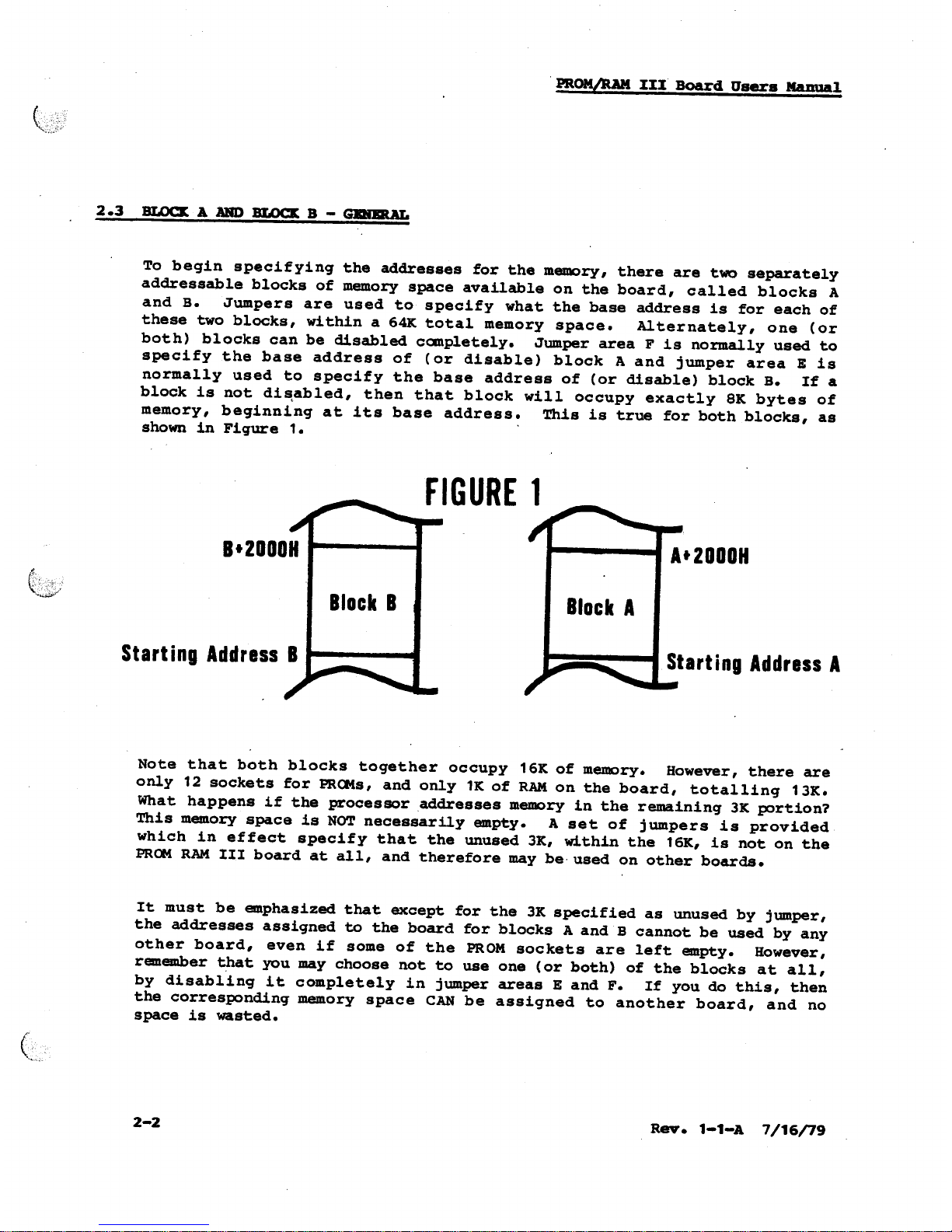
To begin specifying the addresses for the memory,there are two seParately
addressable blocks of memoryspace available on the board, called blocks A
and B. Jumpers are used to specify what the base address is for each of
these two blocks, within a 64Ktotal memoryspace. Alternately, one (or
both) blocks can be disabled canpletely. Jumper area F is normally used to
specify the base address of (or disable) block A and jumper area E is
normally used to specify the base address of (or disable) block B. If a
block is not di~abled, then that block will occupy exactly 8K bytes of
memory, beginning at its base address. This is true for both blocks, as
shownin Figure 1.
FIGURE 1
Starting Address B
Starting Address A
Note that both blocks together occupy 16Kof memory. However,there are
only 12 sockets for PRats, and only 1Kof RAMon the board, totalling 13K.
What happens if the processor .addresses memoryin the remaining 3Kportion?
This memoryspace is NOTnecessarily empty. A set of jumpers is provided
which in effect specify that the unused 3K, within the 16K, is not on the
PRat RAMIII board at all, and therefore maybe-used on other boards.
It must be emphasized that except for the 3Kspecified as unused by jumper,
the addresses assigned to the board for blocks Aand B cannot be used by any
other board, even if some of the PROMsockets are left empty. However,
rememberthat you maychoose not to use one (or both) of the blocks at all,
by disabling it completely in jumper areas E and F. If you do this, then
the corresponding memoryspace CANbe assigned to another board, and no
space is wasted.
Page 14
If the jumpers in area G are switched from the way the board is normally
shipped, then the base address of block Awill be controlled by jumper area
E and the base address of block B will controlled by jumper area F, instead
of the other way around. If this is done, then the address which is
accessed for power-on jump will also be switched, beccining the first address
in block Ainstead of the first address in block B. This is the purpose for
using this option. (See Section 2.14) For simplicity of language, the
Users Guide is written assuming that jumper area Gis left as manufactured.
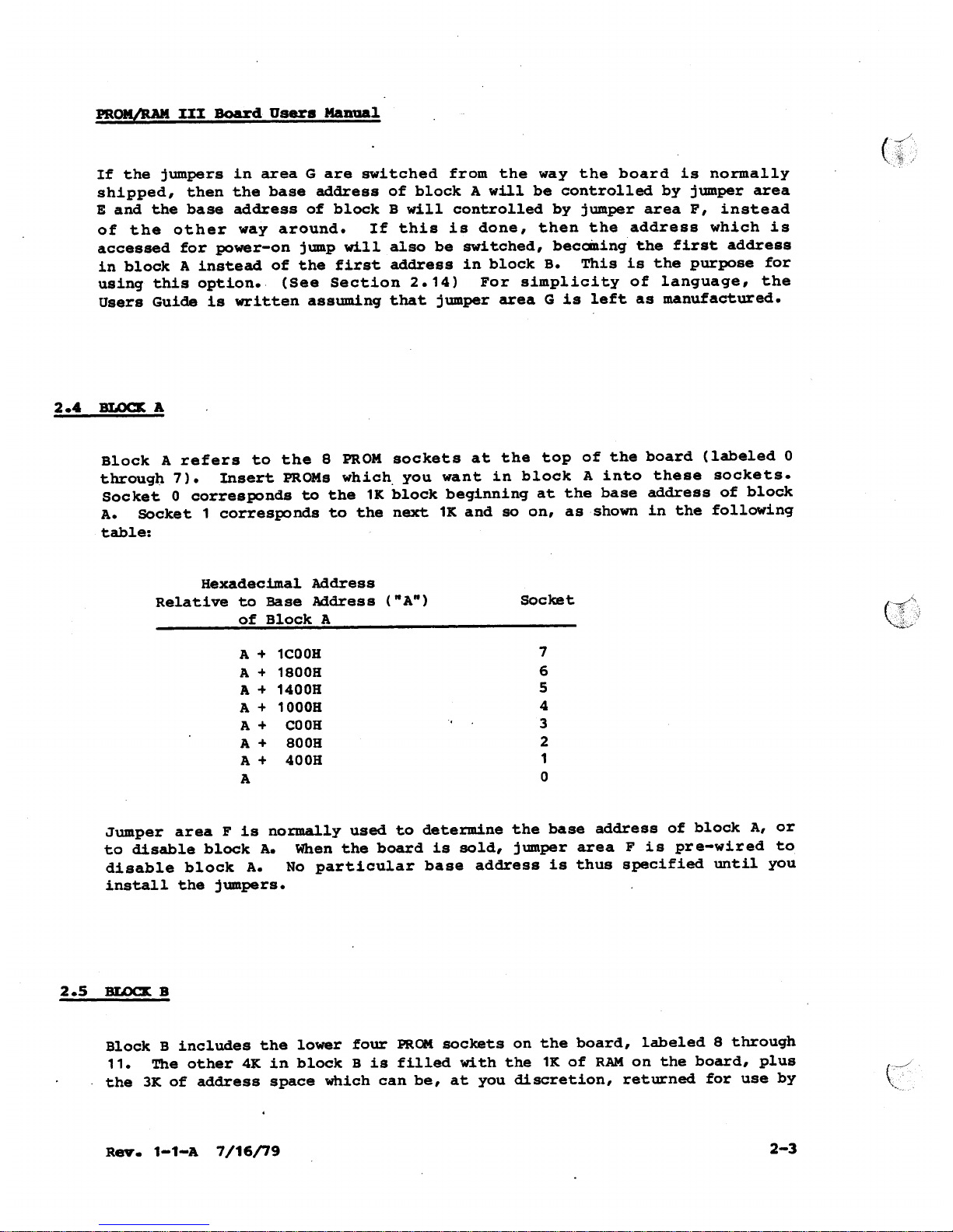
Block A refers to the 8 PROMsockets at the top of the board (labeled 0
through 7). Insert PROMswhich. you want in block A into these sockets.
Socket 0 corresponds to the 1Kblock beginning at the base address of block
A. SOcket 1 corresponds to the next 1Kand so on, as shownin the following
table:
HexadecimalAddress
Relative to Base Address ("A")
of Block A
A+1eOOH
A+1800H
A+1400H
A+1000H
A
+
eOOH
A
+
800H
A
+
400H
A
Jumper area F is normally used to determine the base address of block A, or
to disable block A. Whenthe board is sold, jumper area F is pre-wired to
disable block A. No particular base address is thus specified until you
install the jumpers.
Block B includes the lower four PROMsockets on the board, labeled 8 through
11. The other 4K in block B is filled with the 1Kof RAMon the board, plus
the 3Kof address space which can be, at you discretion, returned for use by
Page 15

other boards. The wayyou specify the address spaces within block B is as
follows: First, you specify the base address of Block B using jumper area E
(or you specify in area E that the block is disabled). If it is not
disabled, then you use jumper area
J
to specify whether the 4Kof PROM
occupies the top or the bottom 4K of the block. These are the only two
choices. The board is pre-jumpered so that the PROMoccupies the lower 4K.
Then, you specffy using jumper area I which 1Kwithin the other 4K is used
for the on-board RAM. Lastly, you specify using jumper area R whether one
of more of the last three 1Kblocks is to be returned for use by other
boards. (Normally you specify that all three of them are returned.)
Twotypical configurations of Block B are shownin figures 2 and 3. Figure
2 is the standard - the one for which the board is pre-wired. Since in the
pre-wired version, block B begins at
COOOR,
Figure 2 shows that the standard
address for scratch-pad RAMis
DCOOH,
and the standard address for the
System's Monitor
PRCM
is
COOOR.
Figure 3 shows the result of putting the
PROMin the upper 4K and specifying that the RAMoccupy the second 1K
portion.
Page 16

ION-BOARD PROMUSCRATCHPAD
(¥')
::e
<=
<=
L.W
<=
L.W
L.W
::E
~
==
=
=
=
<
V)
-
==
c:a..
-
-
=
=
Co:'
L.W
:>
:>
-
••••
I
I
I
I
I.
=
=
=
=
=
=
=
=
e:t
l:I
l:I
e:t
e:t
CI
CI
CI
=rill
e:t
CI
CI
e:t
CI
CI
CI
e:t
._ III
e:t
U
-
•••
CI
U
-
••
--
•••
-
-
-
-
CI
CI
CI
.....
•
•
•
•
•
•
•
•
•••
-
-
-
-
Illl
-
•
-
-
..
CIte
I
I
I
I
C".I
<=
==
::E
~
0
L.W
1.1..1
1.1..1
=
==
c:z:
V)
=
=
=
-
==
=
=
-
-
a..
c.::J
:>
:>
LoW
-
LoA..
, CVdH31VH3S'LWOHd CHV08-NOJ
Page 17

Jumper names: A13, A13, A14, A14, A15, A15 ~ address lines
BA 1, BA2, BAJ • block B address pads
BB1, BB2, BB3 • block A address pads
NOT. The second letter in the block B address pads is "A", while the
second letter in the block A address pads is "B". This occurs because
historically, the pads were named before it was decided to manufacture the
board with the "block swap" jumpers in area G reversed.
Functiom Address lines A13, A14, A15 form the most significant bits of the
address from the CPU. These three bits can select any of 8 possible 8K
blocks of memory in a 64K memory space. see table 1.
Options: Table 2 tells you what jumpers to connect to specify any
Particular 8K block starting address.
ro
I!!.
Functiom The pre-wired connection specifies that the low order 4k bytes of
block B consists of PRCM. This jumper area is used to reverse this, putting
the PRCM at the high end of block B.
Options: If the PROM is to occupy the high order addresses of this block
cut the jumper from 6 to 7 and tie 6 to 8.
Page 18

RAe
0
RA8
0
RA4
0
RAO
18
Function: These jumpers allow the user to selectively determine where the
RAMaddresses are to be located. With the board jumpered as manufactured,
the 1Kof RAMoccupies the top-most 1K of addresses of the 4K scratchpad
memoryblock.
Options: If you wish to alter the factory supplied connections, the
following procedure is recanmended: Cat the jumper from 18 to RAC. Then,
determine the desired address for the 1KRAMfrom Table 3 and connect a
jumper as specified. The third part of Table 3 is not relevent to this
jumper area.
::!i::~
o
17
Function: These jumpers allow the user to selectively determine which 3 of
4 1K blocks of memoryare returned for use by other boards. These jumpers
are selected in conjunction with the RAMmemoryaddress jumper in area I, so
that together, all 4Kof the non-PROM(scratchpad) address space in block B
are accounted for. The factory supplied connections canplement the factory
supplied RAMaddress jumper, so that the bottom 3Kof the scratchpad memory
is allocated for use by other boards.
Options: If it is desired to alter the factory supplied connections, the
following procedure is recanmended: Verify the RAMmemoryaddress selected
previously. Then, refer to Table 3 to find the RAMaddress selected, and
connect jumpers as specified in the third part of the table.
Page 19

A power on/reset jump feature is also provided on this board. When the
iO'C
or PRESET (your choice of which, by jumper selection) line is low, the
instruction stored in the first address of block A or B (determined by the
jumper in area G, as explained below) will be executed by the CPU, and a
"phantom" signal will be issued by the board on bus line 67 which disables
other system memory boards.
After this initial instruction execution, the other memory boards will be
re-enabled. However, if the instruction is a jump to the next instruction
in the same block, then control will have been effectively transfered to
that block on the PROM/RAM III board. Therefore, the second instruction
should be the beginning of a system initialization routine followed by a
systems executive. This is always the case in standard Vector Graphic
computers.
Two additional jumper areas are provided, one to disconnect the phantom
signal if it is not desired, and the other to disconnect the jump to the
on-board PROM if this is not desired. These options give you maximum
control over use of the board.
JTIlo
Function: In the factory version of the board, the
roc
signal is connected
to the power-on/reset jump circuitry on the board. This is appropriate for
standard Vector Graphic canputers, because in these systems, both the RESET
switch on the front panel and the· initial poW'er-on condition cause an active
low pulse on the POC line, via circuitry on the Z80 board. If the CPU board
used in your system does not have this feature, the PRESET signal can be
connected to the power-on/reset circuitry by changing the jumper area D.
Options: To connect PRESET to the power-on/reset dircuitry, cut the trace
between 27 and 28 and tie 28 to 29.
Page 20

rn
Function: When1 and 2 are tied together, the phantom signal is generated
whenever a POCor PRESETsignal is received. Phantomdisables other system
memoryboards. The
zao
(and 8080) processor chip immediately executes the
instruction at
OOOOH
when the
POC
or PRESETsignal appears on the bus,
assuming the CPOboard is so designed. With the other memoryboards in the
system disabled, the PROM/RAMIII Board is free to supply the instruction
for address
OOOoH.
Options: To disable the generation of the phantom signal, cut the jumper
from 1 to 2.
sO
A
Function: Whenthe POCor PRESETsignal is received, a jumper in area A
causes the board to respond to the address
OOOoH
from the CPU. At your
option, you may disable this feature, so that the PRat/RAMIII board is NOT
the board which responds to the address
oOooH.
Options: To cause the board NOTto respond to address
OooOH
when POCor
PRESETis received, cut the jumper from 3 to 4 and tie 4 to 5.
Page 21

611
25 28
Function: With the board as manufactured, jumper area E is used to address
block B, and jumper area F is used to address block A. Furthermore, if the
power-on/reset jump feature is used, the jump will take place to the first
address in block B.
Options: If you want to jumpto block Ainstead, cut the jumpers from 20 to
21 and 25 to 26; tie 20 to 25 and 21 to 26. This change will also reverse
the use of area E and F, so that area E is used to address block A, and area
F is used to address block B.
'1'0
disable the power-on/reset response of the PROM/RAMIII board entirely,
disable both the generation of phantomand the jumpto PROM/RAMIII board.
See Sections 2.12 and 2.13.
Function:
1£
this board is installed in a system without a front pan'el, or
other source of MWRITE,an MWRITEsignal can be generated on board both for
use on board and for feeding back to the bus as a fully buffered S-100
signal. This is not needed in Vector Graphic systems shipped after April 9,
1979, because the Z-80 boards in these systems nowgenerate MWRITE.
Options: If the board is installed in a system without a source of MWRITE,
add a jumper from 9 to 10.
Page 22

Function: The PRDYsignal may be jumpered to the WAITinput in order to
create one wait state each time the board is addressed. This is necessary
whenusing memoryslower than about 300 ns. in a 4 MHz(Z-SO) system. PRDY
is not connected to WAITon the PROM/RAMIII board as manufactured, because
the Vector Graphic Z-SOboard used in Vector Graphic systems generates the
wait-state. You would want to generate the wait-state on the PROM/RAMIII
board if you are using memoryfaster than 300 ns. on other memoryboards in
the system, allowing you to disable the wait state that is built into the
Vector Graphic Z-SOboard (and someother ,manufacturers' Z-SO boards) yet
continue to use a wait-state for the slower memory on the PROMRAM/III
board.
For someZ-SObased CPUboar.ds the WAIToutput is not synchronized properly.
If the WAITis jumpered to the PRDYsignal when such a Z-SOboard is used, a
possible oscillatory condition can arise on the PRDYand WAITlines.
Therefore, caution must be exercised in how this jumper is utilized. The
Vector Graphic Z-SO board has a properly synchronized WAIT,so that with
this Z-SOboard, PRDYmaybe safely tied to WAIT,insuring reliable memory
operation at high speeds.
Page 23

TABLE 1
8K BLOCK (A or B)
A15 A14
A13
STARTlNG ADDRESS
a
0
a
OOOOHa00000
a
a
1
2000Ha81920
a
1
a
4000Ha163840
0
1
1
6000H • 245760
1
0
0
BOOOHa327680
1
a
1
AOOOH ••409600
1 1
a
COOOH ••491520
1 1 1
EOOOH •• 573440
TABLE 2
x ••Block A or B
If
any
Bx1. Sx2. Bx3 is tied
to disable. that block of
memory is di~abled.
CONNECT
DESIRED 8K BLOCK
Bx1
Bx2
Bl(3
STARTING ADDRESS to:
to:
to:
OOOOH
m
m
m
ZOOOH
A13
m
m
4000H
AU
A14
m
6000H
A13 A14
AI;"
8000H
m
m-
A15
AOOOH
A13 A14 A1S
COOOH
m
A14 A15
EOOOH
A13
A14 A15
TABLE 3
ADDRESS OF lK RAM
WITH PESPECT TO THE
,lUr-1PERSFOP.
JU~lPERS FOR
ST.l\RTWG ADDRESS OF
RAM ADDRESS
BUS DISABLE
THE 4K BLOCK
HIiHIN 41(BLOCK
OOOOH 18 to RAO 15 to 16, 13 to 14, 11 to 12
0400H
18 to RA4 15 to 17,
13 to 14.
11 to 12
0800H 18 to RA3
15 to 17. 13 to 16.
11 to 12
OCOOH 18 to RAC
11 to 14 •
13 to 16,
15 to 17
.
Page 24

This board is accompaniedby a program which a110wsyou to program any 2704
or 2708 type EPRCM.Tlle listing of this program is found in Section 2.21,
below. This sameprogram is found on MOOSSystem Diskettes, version 8.4 and
later, which accompanya11 Vector Graphic computers that are equipped with
PROM/RAMIII boards. The program exists on the disk as an immediately
executable utility. The program is written in machine language and is not
dependent on any operating system (except that it uses the Extended Systems
Monitor in Vector Graphic systems for console I/O.) The utility (called
"PROM")runs beginning at address 2BOOHex and takes up less than 1K. If
you want to run it elsewhere, or want to revise it, reassemble it as
described in section 2.20.
If you use an operating system other than MOOS,but you have the MOOS
diskette, sbnp1y load the program under MOOSand copy it to a disk using the
other system. 'l'o load it, just type PROM(return) followed by control-C,
under MDOS. If you do not have the MOOSdiskette, enter the program from
the listing. Once it is loaded in memory, you can execute it from any
executive, inc1uding the Extended Systems Monitor executive. The fo1lowing
explains the use of this program. If you are not using MDOS,then
substitute the MOOScallDlAndsgiven here by those that are relevent to you.
1. Makesure the computer power is OFF. Wait at least five seconds before
pulling out any circuit boards.
3. Find the PROM/RAMIII board. If you cannot easi1y reach PROMsocket 11
with your hand, pull the board out.
4. Insert the PROMyou wish to program in socket 11. This is the
right-hand socket in the second row. Makesure to insert the PROMwith
its notch pointed to the top of the board. The PROMused MUSThave been
erased using ultraviolet erasing 'techniques, unless it is new. The
computer cannot simply write over a'ny previously used PROM,because
programminginvolves turning logical 1's into O's, but cannot go the
other way. Erasing fills the PROMwith 1's, like a new PROM.
5. Return the board to a slot which a1lows you to reach socket 11 without
pulling the board out in the future, if possible.
7. If the system is not in the Extended Systems Monitor executive
(indicated by the Monitor prompt
*)
then depress RESETon the computer
front Panel.
Page 25

depress! on the keyboard. MOOSwill take control, as indicated by the
MOOSpranpt
>.
9. Load the object code to be stored on PROMinto a free area of memory.
Alternately, you may generate the desired code by assembling or
canpilin~ a higher level program.
10. Following the MOOSpranpt
>,
type PROM(return). The PROMprogramming
program will take control.
11. In response to the question "Starting from:", type the address in Hexof
the first location you wish to program, within the block of memory
assigned to PRCMsocket 11. Thenpress the RETURNkey. Usually this
starting address will be CCOo. If programming less than the entire
PROM,it can be any address between CCOOand CFFO. It must be an
address ending in O. If not, the machine will report "bad boundary
address" and give you another chance. Letters must be in upper case.
Donot tack on an Hor any other symbol.
CCOOis the starting address of PRCMsocket 11 if the board is left in
factory-supplied format. If you enter an address outside the range CCOO
to CFFO,the program will not accept it, and will report "out of range"
and then give you another chance. If the addressing jumpers determining
the ~ocation of socket 11 have been modified, you must modify the
program to accept other addresses.
12. In reponse to the question "terminating at:", type the ,address in Hex
of the last location you wish to program, within the block of memory
assigned to PRCMsocket 11. Then press the RETURNkey. Usually this
terminating addresss will be CFFF for 2708 PROMsand CDFFfor 2704
PRaots. If programmingless than the entire PROM,it can be any address
between CCOFand CFFF. It must be an address ending in F, and must be
greater than the starting address. If not ending in F, 'the machine will
report "bad boundary address" and then give you another chance.
As with the starting address, if you enter an address outside the range
CCOFto CFFF, the program will not accept it, and will report "OUtof
range" and then give you another chance. Therefore, if the addressing
jumpers determining the location of socket 11 have been modified, you
must modify the PRCMprogrammingprogram to accept other addresses.
After entering the terminating address, the computer will either
continue with the next question, or it will report "spec;l,fied portion of
PROMis not erased." This message means either that the terminating
address is less than the starting address, or that the PROMis not new
and was not properly erased. This message is strictly a warning,
because in certain rare cases you may want to write over an unerased
PROM. After the message, the system will continue with the next
question. If you want to start over to correct your mistake, instead of
continuing, then depress the ESCkey. This takes the system back to the
Monitor. To get back to MOOSfrom the Monitor, depress
J.
Then begin
the program again at step 10, above. -
Page 26

13. In resp:>nse.to the question "Source address:", type the starting address
in memory of the material you want to store on PR~. This can be any
address in memory. Then press the RETURNkey.
14. Slide the "programming" switch at the upper right-hand corner of the
PR~/RAMIII board to the LEFT.
15. Now, press the RETURNkey again. This will begin programmmingof the
PRCK. The canputer must pass through the range of target addresses 256
times. A message will appear on the screen showing which pass the
machine is currently on.
16. Whenprogrammingis canplete, one of two events will take place. If the
canputer detects no errors in canparing the programmedPRCKwithout the
original code, then the system will return to the MOOSexecutive or
whichever other executive was used to call the programmingprogram. If
an error is discovered however, the screen will showthe first address
within the PRat at which a verification error was found. For example,
if you forgot to slide the programmingswitch to the left, then, since
the PRCKwill not have been programmedat all, the first address will be
incorrect, so that the system will rep:>rt an error at address CCOO,or
whatever was the starting address you had specified. After reporting
the error, the system will return to the MOOSexecutive, so that you can
start over.
17. Whenprogramming is canplete, immediately slide the programmingswitch
on the PRat/RAMIII board to the RIGHT. Donot p:>stp:>nethis.
18. Removethe programmedPRat fran socket 11. Alternately, you mayuse the
PRCKwithout removing it. For example, you may run a checksum of the
PROMusing the Extended System Monitor's
Q
command. To do this, depress
contr6l=Q or whichever other commandyour .system uses to g~t to the
Monitor executive. Then type
Q
CCOOCFFF. (The spaces will occur
automatically.) The checksum, will appear immediately. (If PROMsocket
11 has been readdressed, then use the appropriate addresses.) To return
to MOOSfJ;'an the Monitor, depress ~.
Page 27

Although the PROM/RAMIII board is supplied with a program for programming
PRCfts,this section explains the principles behind the program, (or those
wishing to write their own. The supplied program is listed in Section 2.21,
for reference.
To program a 2708 or 2704type EPRCft,simply write the desired data to the
locations assigned to PROMsocket 11. The board hardware automatically
interprets any writing of data to PROMsocket 11 as an intent to programit.
Youdo not have to program an entire PRCft. Youmayprogram any part of it,
down to blocks as short as 16 adjacent locations. Normally, you will
program all 1Kof a 2708or all 512 bytes of a 2704. Write to all desired
addresses in sequence. After finishing one such cycle, repeat it, using
exactly the samedata. You must repeat this cycle 256 times. In other
words, you must write to each address 256 times, with a substantial delay
between each time you write to each address. This delay is produced by the
time taken to cycle through all the addresses, which is sufficiently long if
16 or more locations are programmed. . .
A good program has a comparison of the source and destination data, after
programmingthe PROMis canplete.
If your system has a dynamicmemoryboard in it (such as all Vector Graphic
systems shipped since about March 1, 1979), then there MUSTbe a delay loop
after each byte is written to the PROM,so that the processor can refresh
memory. The delay loop must execute at least 128 instructions each time it
is accessed. Youwill find an exampleof this at the top of the fourth page
in the listing in Section .2.21.
Before executing a programming procedure, you must slide the programming
switch on the upper right-hand corner of the board TOTHELEFT. Then, put
the PROMto be programmed into socket 11, which is the socket furthest to
the right in the second row. After successfully programming it, slide the
switch BACK. If you do not, you might accidently erase a PROMsitting in
socket 11.
A PROMwhich you want to program must be either newor newly erased using
the standard ultraviolet technique.
Page 28

The source code for the program is listed in Section 2.21 below. Enter the
program using the MOOSeditor LINEEDIT. You can assemble it wherever you
. like, although BCOOis not suggested because M.BASICuses the very top of
RAMfor stack. The pre-assembled version on the diskette (under the name
"PROM") is assembled to run at 2BOO, at the beginning of the MOOS
applications area. The program is less than 1Klong.
You may modify PROM.Sbefore you assemble it, by using the MOOSeditor
LINEEDIT. Onemodification which may be required are the addresses in the
last two lines of PR~. S. Youwill have to change these if you change the
jumpers on the PR~/RAMIII board which assign the address of the on-board
RAM. After entering and modifying the program, SAVEit on diskette under
the namePR~.S. (Type NAME"PROM.S"(return) followed by SAVE(return)
while in LINEEDIT.
To assemble PR~.S, use the ZSMassembler. With a diskette having both ZSM
and PR~.S mounted.in drive 0, and with MOOSin control, type ZSM"PROM.S"
"PROM2""E" (return). The assembler will ask where you want to run the
program. ,Enter the address, for example 2BOOH,that you want it to run at.
Note that if the first character is a letter, it must be preceded by a 0
(zero), and the address must be followed by an H. The above ZSMstatement
will cause the program to be assembled with only errors printed. For other
options possible with ZSM,see Section 4.5 of the User's Guide to Vector
Graphic Systems Using MOOS.
After the assembly is canplete, type TYPE"PROM2"18 (return). This type
will allow you to execute the program simply by typing PROM2(return) while
under MOOS.
If you want to put the PR~ programmingprogram on a PR~, in order to have
a permanent PROMprogramming capability, first choose the memorylocation
you want to give to this PR~, say ~OOO,which is available on the PROM/RAM
III board. Use this address whenasked by the assembler where you want it
to run at. Since there is no RAMat this address, you will have to load the
assembled code into a different location before you can put it on a PR~.
To do this change the type to 00 rather than 18, by typing TYPE"PROM2"00
(return), after the assembly is canplete. This will allow you to type LOAD
"PROM2"2BOO(return) after the MOOSpranpt
>,
thus loading the code atlU\M
address 2BOO,ready to be saved on a PR~.
Page 29

GOOO
0000
0000
0000
0000
oeoo
0000
0000
0000
0000
0000
0000
0000
0000
0000
0000 C003
=
0000 C008
=
0000
0000
0000
0000
CCOO
"
0000 DOFF
"
-
0000 OOOA
"
0000 ooOA
"
0000 0000
=
0000 0080
"
0000
0000 2800
"
0000
2800
2BOO
2800
2eOo E5
2601 05
2802 C5
2803 F5
2804 21 00 00
2807 39
2808 22 03 2E
280B 31 00 DO
280E
280E CO 43 20
2B11 00 OA "
2B13 20 20 20 20
2817 20 20 56 65
2e18 63 74 6F 72
281F 20 47 72 61
2823 70 68 69 63
2827 00 OA
2829 20 20 50 72
282D 6F 60 20 50
2831 72 6F 67 72
2835 61 60 60 69
2B39 6E 67 20 S3
2S30 79 73 74 65
2541 6D
****************************
*
*
*
Prom Programming Program
*
*
Version 1
*
*
for the Prom/Ram III
*
* *
*
by Lance Lewis,
*
*
Vector Graphic Inc.
*
.•. 20-July-79
*
* *
****************************
*
*
*
System equates
.INPUT
OUT
*
*
Definitions
*
PRO'"
BLANK
CRLF
LF
CR
MS6
*
*
Here we go
*
EQU oe003H
EQU oe008H
;character input (COOC on pre 3.0 monitors)
;video driver (C09S on pre 3.0 monitors)
oeCOOH
OFFH
ODOAH
OAH
OOH
SOH
;prom address
;erased byte of prom
;carriage return Linefeed
;linefeed
;carriage return
;most significant bit
'Program to run at?'
ORIG ;assemble here
PUSH
H ;uve HL
PUSH
0
;save DE
PUSH
8 ;saev BC
PUSH
PSW
;save AoF
LXI H,O
DAD
SP
;HL=SP
SHLD STACK
;store it
LXI
SP,OOOOOH
;reset stack
pointer
*
CALL PRINT ;send message
DO
CRLF
DT
,
Vector Graphic'
DO CRLF ;print CRLF
DT 'Prom Programming System'
Page 30

2842 aD OA
2844
*
2844 OA
2845 20 20 50 72
2649 6F 67 72 61
284D 6D 20 70 72
2851 6F 6D
2853 aD SA
2855
*
2855 CD 43 2D STARTADRS
2B58 20 20 53 74
2e5C 61 72 74 69
2860 6E 67 20 66
2864 72 6F 6D 20
2868 SA
2869 CD 4F 2D
2B6C DA 55 28
2B6F CD 43 2D
2B72 aD 8A
2B74 CD 24 2D
2877 DA 55 28
287A CO 96 20
267D DA 55 28
2880 Ea
2861
*
2B81 CD 43 2D ENOADRS
2684 20 20 54 65
2888 72 60 69 6E
2E8C 61 74 69 6E
2890 67 20 61 74
2B94 8A
2B95 CO 4F 20
2B98 DA 81 26
2898 CO 43 2D
289E 00 8A
2BAO CO 24 20
2BA3 DA 81 28
28A6 23
2BA.7 CO 96 20
2BAA OA 81 28
28AO 44
2BAE 40
2BAF
*
28AF 62
2Bao 6B
2BB1 1A TFFS
2882 FE FF
28B4 C2a7 2D
26117 13
2685 CO F6 2C
2SBB C2 B1 2B
2SSE E6 RESTORE
2BBF
*
2e8F CD 43 2D SOURCEAORS
2aC2 20 20 53 6F
2BC6 75 72 63 65
CALL
JC
CALL
OD
CALL
JC
CALL
JC
XCHG
CALL
JC
CALL
DD
CALL
JC
INX
CALL
JC
MOV
MOV
MOV
Mav
LOAX
CPI
JNZ
INX
CALL
JNZ
XCHG
CALL
OTH
LF idown a line
, Program prem'
CALL
OTH
PRINT isend message
I
Starting from :'
AORS
STARTAORS
PRINT
CRLF+MS8
RAN6ERR
STARTAORS
r-IOO
STARTAORS
CALL
OTH
iget start address
iif invalid try again
iprint CRLF
icheck for error
itry
again if error
icheck boundery
ino good
i
OE=start adrs
PRINT isend message
, Terminating at:'
AORS
ENOAORS
PRINT
CRLF+MSa
RANGERR
ENOAORS
H
MOD
ENOAORS
B,H
C,L
H,O
L,E
o
BLANK
BADPROM
o
TEST
TFFS
iget end address
iif invalid try again
icarriage return linefeed
icheck for range error
itry
again if error
iCOl1l\)ensate
icheck boundery
ino good
isave end address
i
in register pair BC
isave start address
i
in register pair HL
iget byte from prom
iis it cLear
iprint "bad prom"
icheck next location
iend of area
imcre to come
irestore registers
PRINT
I
Source address:'
Page 31

2BCA 20 61 64 64
2ECE 72 65 73 73
28D2 8A
2BD3 CD 4F 2D
2BD6 DA 8F·2B
2BD9
*
2BD9 CD 43 2D
2BDC OD OA
2BDE
*
2BDE 00 OA
2BEO 20 20 54 75
28E4 72 6E 20 6F
2BE8 6E 20 74 68
28EC 65 20 70 72
2BFO 6F 67 72 61
2BF4 6D 6D 69 6E
2BF8 67 20 65 6E
2BFC 61 62 6C 65
2COO 20 73 77 69
2C04 74 63 68
2C07 OD OA
2C09 20 20 48 69
2COD 74 20 72 65
2C11 74 75 72 6E
2C15 20 74 6F 20
2C19 63 6F 6E 74
2C1D 69 6E 75 65
2C21 8F
2C22
*
2C22 CD 03 CO STAT
2C25 CA 22 2C
2C28 FE aD
2C2A C2 22 2C
2C2D
*
2C2D CD 43 2D
2C30 00 OA
2C32 OA
2C33 20 20 50 72
2.C37 6F 67 72 61
2C3B 60 60 69 6E
2C3F 67 20 69 6E
2C43 20 70 72 6F
2C47 67 72 65 73
2C4B 73
2C4C 00 iJA
2C4E 8A
2C4F
*
2C4F AF
2C50 32 02 2E
2C53
*
2C53 E5 SAVE
2C54 D5
2C55
*
2C55 7E LOOP
2C56 12
2C57
*
PUSH
PUSH
MOV
STAX
CALL.
JC
AORS
SOURCEAORS
CALL.
DO
PRINT
CRL.F
;10rllat output
Turn on the programming enable switch'
;get source address
;i1 not valid try again
CRL.F
, Hit return to continue?'
CALL.
JZ
CPI
JNZ
INPUT
STAT
CR
STAT
CAU
00
DB
DT
PRINT
CRL.F
LF
, Programming
CRLF
LF+MSS
A
PASS
;check keyboard
;no character
;is it a return
;no try again
;zero
; pass counter
;save source address
;save it
;get ~yte from source
;program it to destination
Page 32

2C57 3E 64
2C59 3D DELAY
2C5A C2 59 2C
2C5D •
2C50 23
2C5E 13
2C5F CD F6 2C
2C62 C2 55 2C
2C65 •
2C65 21 02 2E
2C68 34
2C69 F5
2C6A C5
2C6B •
2C6B CD 43 2D
2C6E OD
2C6F 20 20 50 61
2C73 73 73 AO
2C76 7E
2C77 OE 00
2C79 06 FF LDIV
2C78 04 OIV
2Cn 06 OA
2C7E D2 78 2C
2C81 C6 3A
2C83 F5
2C84 OC
2C85 78
2C86 87
2C87 C2 79 2C
2C8A F1 LOUT
2C8B CD 08 CO
2C8E OD
2CSF C2 SA 2C
2C92 •
2C92 C1
2C93 F1
2C94 D1
2C95 E1
2C96 C2 53 2C
2C99 •
2C99 1A VERIFY
2C9A 8E
2C9B C2 FC 2C
2C9E 23
2c9F 13
2CAO CD F6 2C
2CA3 C2 99 2C
2CA6 •
2CA6 CD 43 2D
2CA9 OD
2CAA 20 20 4E 6F
2CAE 20 65 72 72
2C82 6F 72 73 20
2CB6 64 65 74 6S
2CBA 63 74 65 64
INX
INX
CALL
JNZ
LXI
INR
PUSH
PUSH
CALL
DB
DTH
MOV
MVI
MVI
INR
SUI
JNC
ADI
PUSH
INR
MOV
ORA
JNZ
POP
CALL
DCR
JNZ
LDAX
CMP
JNZ
INX
INX
CALL
JNZ
A,100
A
DELAY
H
o
TEST
LOOP
H,PASS
M
PSW
8
PRINT
CR
, Pass'
A,M
C,O
8,-1
8
10
DIV
10+'0'
PSW
C
A,8
A
LDIV
PSW
OUT
C
LOUT
8
PSW
D
H
SAVE
D
M
YERIFYERR
H
o
TEST
YERIFY
CALL
08
or
idelay for dynamic memory
itime up
ikeep stalling
iadvance pointers
iend of block
ino
keep going
iPointtopass counter
i256
passes
isave Z flag
isave end pointer
iget pass number
iclear number of digits
icompensate for increment
iincrement quotient
isubtract 10 from dividend
ican more be subtracted
iadjust reMainder 0to9 ASCII
iaddtolist of remainders
ione more digit
iprepare for next division
iwas quotient zero
illloretocome
iget a relllainder
iprint it
-iout of digits
ino
then keep printing
irestore end
irestore Z flag
;restore start address
irestore HL
imore passestocome
iget byte from prom
iis it the same
iprint error
iadvance pointers
iend of block
;still more to test
PRINT
CR
, No errors detected'
Page 33

2ceE 00 8A
2CCO
*
2CCO CO 43 20 ·ENO
2CC3 20 20 54 75
2CC7 72 6E 20 6F
2cce 66 66 20 74
2CCF 68 65 20 70
2C03 72 6F 67 72
2C07 61 60 60 69
2COB 6E 67 20 65
2COF 6E 61 62 6C
2CE3 65 20 73
n
2CE7 69 74 63 68
2CEe 00 8A
2CEO
*
2CEO 2A 03 2E
2CFO F9
2CF1 F1
2CF2 C1
2CF3 01
2CF4 E1
2CF5 C9
2CF6
*
2CF6 78 TEST
2CF7 BA
2CF8 CO
2CF9 79
2CFA BS
2CFe C9
2CFC
*
2CFC CO 43 20 VERI FYERR
2CFF 00
2000 3F 20 76 65
2004 72 69 66 69
2008 63 61 74 69
200C 6F 6E 20 65
2010 72 72 6F 72
2014 20 61 74 AO
2018 ES
2019 CO E8 20
201C co 43 20
201F 00 8A
2021 C3 CO 2C
2024
*
2024 7C RANG ERR
2025 FE CC
2027 OA 2E 20
2D2A FE oC
202C 3F
2020 DO
202E CD 43 2D RANGEMES
2031 3F 20 6F 75
2035 74 20 6F 66
2039 20 72 61 6E
2D30 67 65
2D3F 00 SA
XCHG
CALL
CALL
DO
JMP
fIIOV
CPI
JC
CPI
CMC
RNC
CALL
OT
CALL
DT
PRINT
, Turn off the programming enable switch'
LHLO
SPHL
pop
POP
pop
pop
RET
STACK ;retrieve SP
;move it back
PSW ;restore registers
B
o
H
CALL
DB
DTH
;bye-bye
;get end byte
;same as start
;no then return
;Low half same
;return with Z fLag
PRINT
CR
'1
verification error at '
HEX
PRINT
CRLF+MSe
END
A,H
PROM/256
RANGEMES
PROM/256+4
PRINT
'?
out of range
I
;get high address
;valid address
;no print message
;veLid address
;compensate
;return with C in question
Page 34

Aodr 81 82 83 84 E LabeL
Opcd Operand
2041 37
STC
;set error flag
2042 C9
RET
2043
*
2043 E3
PRINT
XTHL
;save HL get SP
2044 7E
LPRINT
MaV
A,M
;get character
2045 CO 08 CO
CAl.I.
OUT
;print it
2048 23
INX
H
;advance pointer
2049 87
ORA
A
;is MSB set
204A F2 44 2D
JP
I.PRINT
;keep sending
2D40 E3
XTHI.
;restore HI. and adjusted
SP
204E C9
RET
204F
*
204F 21 00 00
AORS
I.XI
H,O
;zero' vaLue
2052 CO 03 CO
1.A0RS
CAl.I.
INPUT
;get character
2055 CA 52 2D
JZ
1.A0RS
;is it there
2058 CO 08 CO
CALI.
OUT
;print it
2058 FE 00
CPI
CR
;was it a return
2050 C8
RZ
;thats it
205E 06 :30
SUI
'a'
;reduce to hell
2060 OA 78 2D
JC INVAL
;invaLid entry
2063 FE OA
CPI
10 ;aLpha character
2065 OA 72 20
JC
SAB
2D68 D6 07
SUI 7
;aLpha bias
2D6A DA 78 2D
JC INVAL ;bad character
2D60 FE 10
CPI 16 ;number out of range
206F 02 78 20
JNC
INVAI.
2072 29
SAB DAD
H ;muLtipLy address by
16
2D73 29
DAD
H
2D74 29
DAD H
2D75 29
DAD
H
2076 85
ADD
I.
;combine new vaLue
2077 6F
MaV
I.,A
2078 C3 52 20
JMP
I.AORS
;keep going
2078
*
2078co43 20
INVAI.
CAU PRINT
207E 00 OA
DO
CRI.F
2080 :3F20 69 6E
'OT '1 invalid response'
2084 76 61 6C 69
2088 64 20 72 65
208C 73 70 6F 6E
2D90 73 65
2092 00 8A
00
CRI.F+MSB
2D94 37
STC
;set
error flag
2095 C9
RET
2096
*
2096 7D
MOD
MOV
A,I.
;get Low byte
2D97 E6 OF
ANI
OFH
;mask Low nibbLe
2099 C8
RZ
;if zero fine
209A CD 43 20
CAU
PRINT
2090 3F 20 62 61
OT '1 bad boundery address'
20A1 64 2G 62 6F
20A5 75 6E 64 65
20A9 72 79 20 61
2DAO 64 64 72 65
2D81 73 73
2D83 00 8A
DO
CRI.F+MSB
Page 35

2065 37
20B6 C9
20B7
20B7 CO 43 20
20BA 3F 20 73 70
2DBE 65 63 69 66
20C2 69 65 64 20
2DC6 70 6F 72 74
20CA 69 6F 6E 20
2DCE 6F 66 20 70
2002 72 6F 6D 20
2006 69 73 20 6E
200A 6F 74 20 65
2DDE 72 61 73 65
2DE2 64
2DE3 00 SA
20E5 C3 BE 2B
20ES
20ES 7C
20E9 CO ED 2D
20EC 70
2'oED
20EO CD FO 20
2DFO
2DFO OF
20F1 OF
20F2 OF
2DF3 OF
20F4 F5
2DF5 E6 OF
20F7 C6 90
2DF9 27
20FA CE 40
20FC 27
2DFD CD OS CO
2EOO F1
2E01 C9
2E02
2E02
2E03
•
SYTE
•
NIBBLE
PASS
STACK
CALL
oT
I'IOV
CALL
ll10V
CALL
RRC
RRC
RRC
RRC
PUSH
ANI
ADI
DAA
ACI
D.AA
CALL
POP'
RET
PRINT
'?
specified portion of prom is not erased'
CRLF+MSB
RESTORE
A,H
BYTE
A,L
;first the high byte
;print hex byte
;now the low byte
;save A
;mask high nibble
;super short-cut
;technique for converting
;binary to ASCII
;ala HB
;print it
;restore A
Page 36

Address input lines AO to A9 are buffered in line receivers U13 and U14.
The outputs of U13 and U14 are then connected to both the PROM and RAM
memory address pins. Address input lines A10 to A15 are buffered in U12
before use on the board. Lines A10 to A12 are inverted by the buffers
and used as inputs to decoders U8 and U9. These three lines enable one
of eight outputs on U8 or U9, depending on which decoder is enabled.
Note that since A10 to A12 are inverted, the decoding sequence is
reversed. When A10 to A12 are all "0", the number 7 output of the
enabled decoder is selected. Each of the eight outputs from each
decoder is used to enable a specific 2708 PROM or the 1K block of
on-board RAM, or one of the three 1K segments which are not used on this
board.
Address input lines A13 to A15 are used to enable one or the other
decoder. Jumper Areas E and F determine which specific 8K block of
memory corresponds to each decoder. The decoders are enabled by the
output of U18-13 and U10-6. (They are enabled when their
0
input is a
logic low "0".) Which decoder is enabled by which line depends on the
jumpering in Area G. Jumper Area G can be used to switch the memory
blocks thus assigned to each decoder.
Inversion of the on-board PROM and scratchpad memory address within
block B may be accomplished by changing the jumper in Area J. This
jumper determines whether or not the A12 address line is inverted by
U11-4 before being used by decoder U9.
Selection of which 1K segment of the memory space will be assigned to
the on-board RAM and which three 1K segments will be returned for use by
other boards is handled by U9 outputs pi.ns1, 2, 3, 4, gate U10-12 and
jumpers in Areas I and H. Any time an input to gate U10-12 goes low,
this board is inhibited from putting data on the
01
bus by forcing the
01
line drivers to the high impedence state. Therefore, the three
outputs of U9 which are connected to the inputs to U10-12 cause output
.from this board to be inhibited when one of the corresponding addresses
appear on the address bus. Likewise, whichever U9 output is tied to the
CE input to the RAM will enable the on-board RAM when that address
appears.
Page 37

The DOlines fran the S-100 bus contain data fran the CPUto the memory.
RAMis contained in two 2114 chips (U1 and U2). 01 contains the low
four data bits in each location and U2the high four bits. Thus 000 to
D03are tied to the data pins of U1and 004 to D07to the data pins of
02. These data bus lines are also tied in parallel to the eight data
lines of each 1Kbyte PROMchip.
Data outputs from the RAMand PROMare connected to the input of a
tri-state line driver U16or U17. This parallel bussing of outputs fran
the memory chips is possible since all data outputs on the chips are
tri-state.
U15 buffers the data lines inputting to the board. This buffer is
enabled so long as U5-10 is low, which is true if U4-11 is high, which
is true if either the on-board RAMis being written to or if PROMsocket
11 is being written to. This logic is accanplished as follows. U4-6 is
the NANDof MWRITEand the inverted (active high at U5-4) chip select
for PROMsocket 11, so that U4-6 is low if both PROMsocket 11 is
selected and MWRITEis active. U20-6 is the NANDof MWRITEand the
inverted RAMchip select (active high at U5-13) so that U20-6 is low if
both RAMis selected and MWRITEis active. Since U4-11is the NANDof
U4-6 and U20-6, U4-11will be high if either U4-6 or U20-6 is low.
Writing of data into the RAMis controlled by MWRITE.Dependingon the
jumper in Area S, MWRITEcan be taken fran the bus (if a front panel is
used or if there is another source of MWRITEin the system), or it can
be generated fran SOU'!'andPWRon this board. To generate MWRITEon the
board, when SOUTand
PWR
are both low, U18-10is high. This signal is
buffered at U14-9and is available both to the bus and the board as
MWRITE.MWRITEis NANDEDwi~h the RAMchip select (inverted to active
high at U5-13), giving the RD/WRsignal for RAM. Whyis this necessary,
since the signals are combinedwithin the 21141 It is not necessary in
order to generate RDiWi,but to enable the data bus input driver U15, as
exlained above, we needed external active low signals specifically for
writing to RAMand to PROM.Rather than putting another inverter on the
board, the same signal is used for RD/WRto RAM. Alow on RD;WRputs
the chip in the write mode. Data on lines 000 to 007 will be written
Page 38

into the RAMs,assuming the board has been addressed and the RAM
selected by the chip enable from Area I.
Whenit is desired to read data fran this board, the U19-6 must be low
at the appropriate time, enabling the
01
bus drivers U16and 017. This
is accomplished by generating the logic NANDfunction of numerous
signals. Wheneither block A or block B is selected, the output of
020-3 is high which is used as one input to 019-6. Another input to
019-6 is generated by SMEMRwhich indicates that a memoryread is to be
executed. SMEMRis inverted at U11-2, then gated through U18-1, before
being connected to U19. To allow selective disabling of this board's
data outputs for any of the three unused 1K memoryblocks, the chosen
chip select lines are connected to U10 pins 1, 2 and 13. So long as
they are high (not active), then U10-12is low. In combination with a
low from U11-2 (inverted SMEMR),a high appears on U18-1, which goes to
U19-1. Another input to U19-6is £ran U18-4which senses that both SOUT
and SINP are low. The last input to U19-6is PDBIN. Whenthis signal
is high it indicates that the
01
lines are in the input mode.
Therefore, whenall foUr inputs are high, indicating on board memorycan
be read, U19-6will go low, thus enabling the data output buffers U16
and U17.
The poweron/reset jumpfeature is initiated by the POCor PRESETinput
(jumper option in Area D). Disabling of other system memoryboards
during the power on/reset jump is accomplished by the PHANTOMoutput
from this board, assuming the other boards are so wired. Thepower
on/reset feature is provided by an RSflip-flop in U20, with the
P'OC
or
PRESETline from the bus connected to the set input (U20-9) of the
flip-fop. The PHANTOMsignal is generated by the U20-11 active low
output, and the 020-8 active high output is used to set U18-13low, thus
enabling U8or U9, depending on the jumper in Area G. Since the address,
on the 'bus will be 0000, this causes the processor to execute the first
instruction in the enabled 8Kblock. If this instruction is a jump to
the next instruction in the sameblock, then whenthat instruction is
decoded causing a low at U10-8and hence at U20-13, the flip-flip will
reset and cancel the PHANTOMsignal.
The PReYsignal can be tied to the WAITinput by jumpering Area K. If
so, the PReYdriver is enabled wheneverthis board is addressed and the
processor is not doing I/O (determined by U19pins 9, 10, 12 and 13.)
WAITis low at this time, thus PReYgoes low, putting the processor in a
wait state. This makesWAITgo high, so that whenthe next clock cycle
occurs, PReYgoes high again. The result is a one-cycle WAITstate each
time the board is addressed. Note there is an error in this logic: a
wait state will be generated (if jumpered in AreaK) so long as any part
of blocks Aor B are addressed, INCLUDINGthe 3Kwhich are used by other
boards. This other 3K may be a function such as video or disk
controller, which should not have a wait state.
Page 39

PROMsocket 11 is used to program an EPROM.EPROMsare programmedas
follows: With the desired data on the data inputs to the. PROMand the
desired low order address byte on the address lines to the PROM,chip
select must be raised to 12V(rather than the usual 0 for reading and 5
for not-select.) Then after ~ delay of 10 micro-seconds, a 26Vpulse on
the chip's programmingpin (pin 18) must occur for 400 micro-seconds.
The CPUmust be held in a wait state during this time, as well as an
additional 1/2 micro-second. This will proqram one byte ONCE. Proper
programming of 2708 EPROMsrequire that each byte be programmed256
times, with a delay after each time. This is handled in software, which
should program all the locations on the PROMonce, and then repeat the
cycle 256 times. Software does not have to send any special signal for
programming a PROM,since hardware will interpret any memorywrite to
the PROMas an intent to· program it. unintential writing to the PROM
will thus cause programmingif the 26Vsupply is accidently left on.
U3contains two one-shots which are used to generate the timing for the
programmingpulse. Each of these one shots has different Rand C values
connected to it, creating different length pulses. A 10 micro-second
active low pulse is generated at U3-4 and a 410 micro-second active high
pulse is generated at U3-5. Whenthese two are NANDEDtogether at U4-3,
the result is a 400 micro-second active low pulse following a 10
micro-second delay, as desired. This pulse begins whenPSYNC(bus line
76) and clock-1 (bus line 25) are NANDEDat U4-8 and put into U3-1 and
U3-9, and at the same time the PROMsocket 11 chip select arrives at
U3-2 and U3-10. They will only fire if it is not a memoryread cycle,
because U11-2 keeps the one-shots reset (via reset pins U3-3 and U3-11)
if SMEMRis active.
The low-high transition of the 410 micro-seond pulse at U3-5 generates
an active low on XRDY(bus line 3) by inverting it at U6-2, in order to
put the CPUin a wait state. This stays low for 1/2 micro-second after
the pulse is over because of an RCdelay tied to U6-2.
The 400 micro-second pulse is converted to active open at U6-10 and
U6-12. The program pulse of 26V is then generated by a 2N3643
transister, using a supply voltage from U7and related circuitry. U7is
turned on by the sliding programmingswitch. This switch must ONLYbe
on whenprogr.amminga PROM,because erroneous writing to that PROMwill
otherwise alter it whennot desired.
Page 40

When the pulse is over and the wait line is released, the CPU is
released to increment the address and program the next byte.
Power for this board is obtained from the unregulated
+8V
and plus or
minus
18V
supplies in the system.
Regulation of the input vo1ta98 to the required
-SV
and
+12V
is obtained
by the,use of four three-terminal regulators. Dual regulators are used
to insure ample supply current. The
+SV
supply is regulated by one
regulator. Bypass filtering on all power lines is accomplished by
multiple electrolytic capacitors for each supply voltage. This
filtering insures stable noise free operation of the board. C;:apacitors
are also used on each regulator input for high frequency bypassing and
regulator stability.
The
+26V
programming supply is produced from the
+12V
regulated supply
by a TL497 switching voltage regulator in a low-power step-up
configuration, using a1mH coil.
Page 41

5 r;}6 ~;
c;:;]u
JtJ~)
I·
•• :I ••••••• • •
..~<E!)r;"iiI. •
s::
fit
CJ
L:...:.J
~r:tJ~. ·
;>••••••
'1 • •
~:
;
~....
.
.
· f I :. ~
t....:·~~:::'
>:: : : : ::r '. ·
•• •• •• • • •• .., •• •• ••• :l..... •• •••••••
..
.
...•..•..•..•..•...•...•.....•..
•••••••••••• • ••••••• •• 5) •
I. ~
f
I
li!)
I~. •••••••• ~
..
.
'.. ':
:-
•
l:l. ••• •.••••••••••
•-.-.-.-.-.-. -. -.-. -.-. + •• •
5)
I --:
•••••••••••• ~:t : ••••• :. •• •••• •
It
0 -:
f
-"'.... • •••••••••.
Oft . •
It •••
0... ...••5)0
I
0 :
-------.--!.
A • )
gO •••••••••• 0
.~t
•• • • • • •• •• •• !::! •• • • •• •• •
O. 0
•••• 0 0
••••••••••••• •• ••••••• O' •••••••• . 0
f
I
·
I
5) \-
0
•.
0
0O~""''''
S. •• •••••• ~
;0:-,0
_ • ,0.
0
• • ~ 0
••••••••••••• 0
0
00 0 0 ••••••••• '1lr
. 0 0
5)
I ;
·c:::::::](-:...:...:-:...:-:-;....:-;-:-)r ·5;:::::'::; ,,~~.~
•. ••••••• 00
•••••••••••• •••••••••••• • 00. 0
f
•
II I ••
•• Q
.sf
I •••
- 1••••••
0 •••
•-.-.-.-.-.-. -. -.-.-.-. .-.-.-.-.-. -.-.-. -.-.-. 0 •••
............ 0....... . .
- f 11 __ 1
i
=~~:':·f!~
1-:-:1
•••••••••••• •••••••••••• ' •••••••• ell ••
•••••••••••• •••••••••••• 0
.n
0
I. •
of'
····1f·1·
~:::::r:
O~+
T
••• •••• • •• •• • •• ••• •• •••• 0
o!
>'"
to • "
___ >l.
f........ .....••.
e
~ J-.+
>t •
r-+ • • + .,
(r-.-).-
i o. 0
t.:!ee5 e)
i~;;;;:'
Page 42

Page 43

to
U5 13
4~
~~I
12
5 13- 8 •.
MWRITED
68
~"~"."o
PWRD 77
8
,0r.:-".9W
91UI8
10
~4
5
U4
6 ~SOUT
45
809~ ~
74LS02
T
3 ~ 1
8T97
MWRITE
10
8
10
8
~~7
5 RCiWR CS
RllIWR
cg
------l
A0 UI3.J'"
AO
c-!I
AI .
Al'I
14 13 13
AI
~~ ~
+12
A2 81 10UI 9,1'
A2
A3-31 2
3
4
A3
R4
.~ [' lie:;
UI
U2
L5K
A4
~ A4
2114 2114
~4
A
A5-291~t..- 41'3 5
2 A5
;~ ~
A6 UI4 5
I A6
R3
A7-
83
61;;14
17A7
IK
I
A:~~~7
16AS
~
3
Il'...
15A900 01 02 03
A9L.? I
-;rl~
II
04 05 06 07
14 13 12 II 14
13
12 II
Foo
,~44~
000 2 5 18
001 35 ~16
00~~'1414
003D89 8~12
--l
004-38111' 9 c:;
00~~39 [:::; 131:' 7
I
00;~5 ~
007090 I~ 3
~.~
.
-
'ff~219
.u
7 A0001J:q:
AI 01 "
A202 I
A30 I
A404 I
PROMS
~i
I
2704/2708
A70
AS
tl
A9
0
i-
I~
2or--
.Ll
,J-.1
-
l--
-
Co--
-
I-
- -
'--
-
-
'---
-==
-
L-
-
L--
-
-
+=;
~~
74LS04
AIO- 37
"
10
_ 87
[5-
I~
VCC
9 5
Al' •.•.
9 2 8
16
76
f.
A12;:;; 33
3~ 4
[;7
2
~I
8
U8
t:?
AI3
ro==o=
OISASLE
I ,,,-
---
~LSIO
-
V
15~ 14
'
AI4
86
AI5
32
PI
A
PRESET
11_
Page 44

+-8V 51
•. T CI9 •. T CI
r...l.
3.3UF
T...l.
25UF
T
50VT50V PSYNC
\7 \7
76r--.: 9
- •..•..••... ~U4
25~
1/)1
74367
~
4
'\7
+
n
.....J
,..L......1
-
l..-
e--
-
-
'---
-
-
1-
-
-
~~
~~
VCC 9 7 4 312fl
#
7 65 4 3 2 I I/)I;PROMS
8 U9 74LS42 8-11
ABC 0
IS 141 131 121
I
7
JU:1
R2
CIS 181<
,~~
14.1-- IS
I
o~
2
U3
74221
T
9 74LS20
~UI9~
¥-
~=I
8K BLOCK SWAP
I~ 78 UI7
:
~46 U6-2~11
6 UI8 4
"I.A<
r
4SS~ 74LS02 I
r~
27 14~13 1nK,;l72~PROY
EXTERNAL ~
'AIT GENERATION 74367
RI
C20i 15K
.047i
~S
~ !o
--!2
U3J
7422]1
i
iQ~
-W-
U1t-2
8097
6 UI
7
l:A-
6~7
i
41'-... S
.~
'''~,''
l~
Ik~1I
.'~
2t:r3
il7L
I
I..-
'--
-
-
I--
I---
I
+~
I
lOAn
RA4
R
~
I? 6
UI9
151 •
74LS20
SWI
r
~+12
6.8
~
~1411
2 +S
I
R9
4.7K
II f:':::...._2· IOOpF
~~_ R8 C27
.001
I.
1.21K 1
% ~
C22
V
R6
U9-12'--- 24.9KI°1.
9Sc-l01e
94<:1011
4'<:]012
42<'1DI3
91<'1014
92.cJ01S
93:::016
43~017
C26
+1
4.7
l/
~Kr--
(f
VOl
r-.2N3643
~'2
~'O
L-
-
-
-
U~3-3'" 2 2 II ~4LSO:~SMEMR
13 I
21
3 UI8
I UIO
12 74Ls02
74LSI0
-
....•...
VECTOR GRAPHIC
;:;: .•Z;],~
WESTLAKE VILLAGE
CALIF.
mu
i
PROMtRAM m
12 K
1
~
REV-O
7-13-79
A
SillIad: ••••.. 110.jDWS. IKI.
.........
E .'
..
"
•••u
3
 Loading...