

Page 1
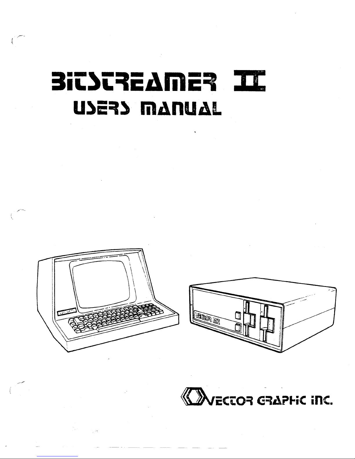
:lit)t=tiCAli1iC=I
JI
U)E=I) mAnUAL
Page 2

Page 3
BITSTREAMER II BOARD
Revision 1
USER'S MANUAL
Revision A
January
1, 1980
Page 4
Copyright
198~ by
Vector Graphic Inc.
All rights reserved.
Disclaimer
Vector Graphic makes no representations or warranties with respect to the
contents of this manual itself, \\bether or not the product it describes is
covered
by
a warranty or repair agreement. Further, Vector Graphic reserves
the right to revise this publication and to make changes from time to time
in the content hereof without obligation of Vector Graphic to notify any
person of such revision or changes, except \\ben an agreement to the contrary
exists.
Revisions
The date and reV1Slon of each 'page herein appears at the bottom of each
page. The revision letter such as A or B changes if the MANUALhas been.
improved but the PRODUCTitself has not been significantly modified. The
date and revision on the Title Page corresponds to that of the page most
recently revised. When the product itself is modified significantly, the
product will get a new revision number, as shown on the manual's title page,
and the manual will revert to revision A, as if it were treating a brand new
product. EAai MANUALSHOULDONLYBE USEDWITHTHEPRODOCTIDENTIFIEDONTHE
TITLE PAGE.
Page 5
'Ibe Bitstreamer II Board sold hereunder is sold "as is", with all faults and
without any warranty, either expressed or implied, including any implied
warranty of fitness for intended use or merchantability. However, the above
notwithstandi1'l3,VEC1'OR GRAPHIC, INC. ,will, for a period of ninety (90)
days following delivery to customer, repair or replace any Bitstreamer II
Board that is found to contain defects in materials or workmanship,
provided:
1. Such defect in material or workmanship existed at the time the
Bitstreamer II Board left the VECTOR GRAPHIC, INC., factory;
2. VECTOR GRAPHIC, INC., is given notice of the precise defect
claimed within ten (10) days after its discovery;
3. The Bitstreamer II Board is promptly returned to VECTOR GRAPHIC,
INC., at customer's expense, for examinationbyVECTOR GRAPHIC, INC., to
confirm the alleged defect, and for subsequent repair or replacement if
found to be in order.
Repair, replacement or correction of any defects in material or workmanship
which are discovered after expiration of the period set forth above will be
performed
by
VECTOR GRAPHIC, INC., at Buyer's expense, provided the
Bitstreamer II Board is returned, also at Buyer's expense, to VECTOR
GRAPHIC, INC., for such repair, replacement or correction. In performing
any repair, replacement or correction after expiration of the period set
forth above, Buyer will be charged in addition to the cost of parts the
then-current VECTOR GRAPHIC, INC., repair rate. At the present time the
applicable rate is $35.00 for the first hour, and $18.00 per hour for every
hour of work required thereafter. Prior to commencing any repair,
replacement or correction of defects in material or workmanship discovered
after expiration of the period for no-cost-to-Buyer repairs, VECTOR GRAPHIC,
INC., will submit to Buyer a written estimate of the expected charges, and
VECTOR GRAPHIC, INC., will not commence repair until such time as the
written estimate of charges has been returned by Buyer to VECTOR GRAPHIC,
INC., signed by duly authorized representative authorizing VECTOR GRAPHIC,
INC., to corrunence
wit.11
the repair work involved. VECTOR GRAPHIC, INC.,
shall have no obligation to repair, replace or correct any Bitstreamer II
Board until the written estimate has been returned with approval to proceed,
and VECTOR GRAPHIC, INC., may at its option also require prepayment of the
estimated repair charges prior to c~ncing work.
Repair Agreement void if the enclosed card is not returned to VECTOR
GRAPHIC, INC. within ten (10) days of end consumer purchase.
Page 6

Page 7
This manual is intended for computer
distributors, or others with at least a
moderate technical knowledgeof small
computers.
It will describe what the Vector Graphic
Bitstreamer II Board does in the context
of a computer system, howto use the board
both in Vector Graphic and in other
5-10(3
systems, and howthe board circuitry ¥.Orks.
Each section is written at a uniform level
of technical depth. "Perspective" describes
WHATthe board does and requi res only a
rooderate knowledgeof computer design.
Most other sections tell
HCNl
to makeit do
things and assl1!t"esthe same level of
knowledge, plus the ability to solder
jumpers and flip switches. "Theory of
Operation" discusses WHYthe board ¥.Orks
and assumesa knolwedgeof digital
electronics.
Page 8

Page 9
1.1
1.2
1.3
1.4
1.5
1.6
1.7
1.8
1.9
1.1".1
1.11
Introduction ••••••••••••••••••••••••••••••••••••••••••••••• 1-1
Serial channels generally •••••••••••••••••••••••••••••••••• 1-1
Serial asynchronous communication •••••••••••••••••••••••••• 1-2
Serial synchronous communication ••••••••••••••••••••••••••• 1-2
Interrupt driven serial channels ••••••••••••••••••••••••••• 1-3
RS-232C theory ••••••••••••••••••••••••••••••••••••••••••••• 1-4
RS-232C on the Bitstreamer II •••••••••••••••••••••••••••••• 1-5
2~
mA current
loop•••••••••••••••••••••••••••••••••••••••••
1-7
Real time clock interrupts ••••••••••••••••••••••••••••••••• 1-7
Interrupt vectors and priority ••••••••••••••••••••••••••••• 1-8
Parallel channels •••••••••••••••••••••••••••••••••••••••••• 1-9
Page 10
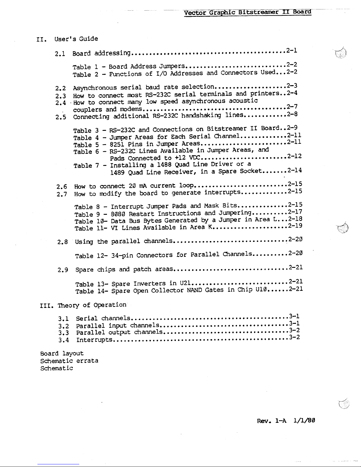
Table 1 - Board Address Jumpers •••••••••••••••••••••••••••• 2-2
Table 2 - Functions of I/O Addresses and Connectors Used •••2-2
2.2 Asynchronous serial baud rate selection •••••••••••••••••••• 2-3
2.3 How to connect most RS-232C serial terminals and printers ••2-4
2.4 .How to connect many low speed asynchronous acoustic
couplers and modems ••••••••••••••••••••.••••••••••••••••••• 2-7
2.5 Connecti~ additional RS-232C handshakill3 lines •••••••••••• 2-8
Table 3 - RS-232C and Connections on Bitstreamer II Board ••2-9
Table 4 - Jumper Areas for Each Serial Channel ••••••••••••• 2-ll
Table 5 - 8251 Pins in Jumper Areas •••••••••••••••••••••••• 2-l1
Table 6 - RS-232C Lines Available in Jumper Areas, and
Pads Connected to +12 VDC •••••••••••••••••••••••• 2-12
Table 7 - Installill3 a 1488 Quad Line Driver or a
1489 Quad Line Receiver, in a Spare Socket ••••••• 2-l4
2.6 How to connect 20 IDA current loop •••••••••••••••••••••••••• 2-l5
2.7 How to modify the board to generate interrupts ••••••••••••• 2-l5
Table 8 - Interrupt Jumper Pads and Mask Bits •••••••••••••• 2-l5
Table 9 - 8~80 Restart Instructions and Jumpering •••••••••• 2-l7
Table 10- Data Bus Bytes Generatedbya Jumper in Area L •••2-18
Table 11- VI Lines Available in Area K ••••••••••••••••••••• 2-l9
Table 13- Spare Inverters in U2l ••••••••••••••••••••••••••• 2-2l
Table 14- Spare Open Collector NAND Gates in Chip U10 •••••• 2-2l
III. Theory of Operation
3.1 Serial
cha.nn.els •••••••••••••••••••••••••••••••••••••••.•••••
3-1
3.2 Parallel input channels •••••••••••••••••••••••••••••••••••• 3-l
3.3 Parallel output channels ••••••••••••••••••••••••••••••••••• 3-2
3.4 Interrupts•••.••.•••••••.•••••.•••••••.•.•.••••.•..•••••.•.3-2
Board layout
Schematic errata
Schematic
Page 11
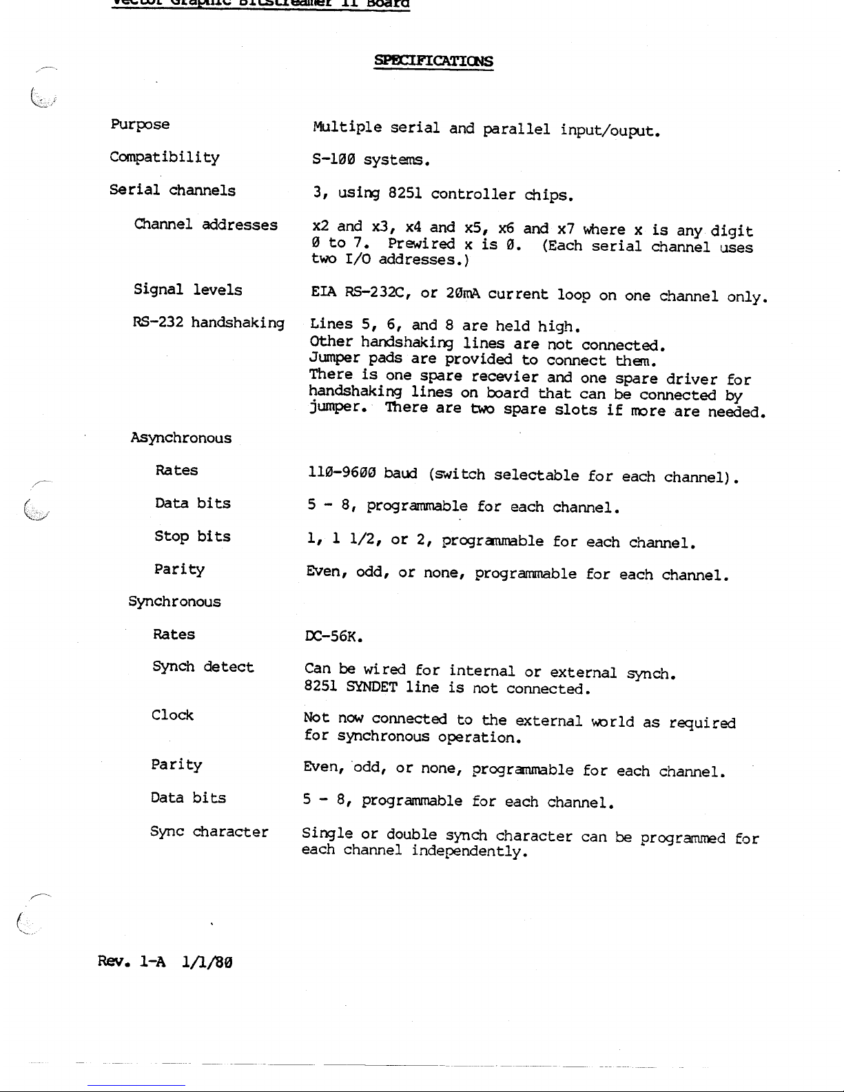
Purpose Multiple serial and parallel input/ouput.
Compatibility S-1~0 systems.
serial channels 3, using
8251
controller chips.
Channel addresses x2 and x3, x4 and x5, x6 and x7 where x is any digit
o
to 7. Prewired x is 0. (Each serial channel uses
two I/O addresses.)
Signal levels EIARS-232C,or 201Mcurrent loop on one channel only.
RS-232handshaking Lines 5, 6, and 8 are held high.
Other handshaking lines are not connected•
.Jumperpads are provided to connect than.
There is one spare recevier and one spare driver for
handshaking lines on board that can be connected by
jumper. '!here are two spare slots if rooreare needed.
Can be wired for internal or external gynch.
8251 SYNDETline is not connected.
Not nowconnected to the external ~rld as required
for synchronous operation.
Single or double synch character can be programmedfor
each channel independently.
Page 12
TTL
(input
= 1 'ITL
load; output drives 5
TTL
loads).
8 input, 8 output for each channel.
+5 VDC, +12 VDC, -12 VDC, and GND are also provided
for each channel.
Over l00K bytes/second.
Optional. Has 34-pin female connector and 34-line
ribbon cable. No connector is at the other end,
allowing user to configure as required. Must be
ordered separately.
If you are using the USARTs on the board as sources
of interrupts, you cannot use the output side of
Parallel O1annel A for normal parallel output.
Interrupts can be generated fram any combinaton of
the 3 USART RxRDY's, 3 TxRDY' s, and a 55 Hz real time
clock. Jumper pads provided. None prewired.
Output to parallel channel A selects (masks) interrupt
sources previously wired in.
Dummy input from Parallel Channelaresets 55 Hz real
t~e clock interrupt line during an interrupt service
routine. However, Parallel Channel B can be used for
normal input (and output) as well.
Can use 8080, 280 Mode 0, 280 r~de I, or 280 Mode 2
A Bitstreamer II board can generate one of 9 possible
bytes in response to an interrupt, including
three of the restart instructions for usewith 8080
and Z80 Mode 0 interrupts. Software polls to
determine which possible source on a Bi tstreamer II
board is the actual source of the interrupt.
S-100 interrupt bus Pads are provided for jumpering interrupt sources to
the S-100 VI lines.
+8 Vdc@720 mA typical.
+16 Vdc@30
IDA
typical.
-16 Vdc@30 IDA typical.
Page 13
The Vector Graphic Bi tstreamer II Board is an all-purpose input/output
board for S-l~~ systems. It offers three serial I/O channels and 2 8-bit
parallel input/output channels for interfacing with multiple peripheral
devices such as printers, modems, and terminals. It also offers a 55 Hz
real-time clock which can interrupt the CPU for functions such as sharing of
the CPU by several users or peripherals.
We will use the term "channel" rather than "port" to avoid confusion
causedbythe fact that each serial channel makes use of two I/O addresses,
which are often called I/O "ports."
The CPU sends data to the serial and parallel charmels via I/O addresses.
The I/O addresses used by the board can be changed as a group. The board
uses the eight I/O address x2 to x9 (in hexadecimal notation), where x is
any dig it from 0 to 7. You specify the value of x
by
jumper, as listed in
Table 1 in Section 2.1. Table 2 in Section 2.1" lists the function of each
of the eight I/O addresses, which are fixed relative to one another.
'!heBitstreamer II Board does not come wi th any software for specific
applications, though Vector Graphic supplies certain items of software that
make use of its featues.
The three serial channels center around three industry standard 8251
USART (Universal Synchronous/Asynchronous Receiver!Transmitter) chips. Much
of the flexibility of the Bitstreamer II board derives from the flexibility
of these chips, which can be modified via software. You, through software,
can control the rate of transmission, and the format of the transmitted
data. Data is transmitted as ASCII code having bet'II'Ieen5 and 8 bits per
character, with an optional added-on pari ty bi t (choice of even or odd), and
with one start bit and a choice of one, one and a half, or two stop bits per
character. Further, using the 825l's, the board can handle either
asynchronous or synchronous comm.mication. Each serial channel is entirely
independent of the others. Baud rates, format, handshaking, and whether
comnunication is asynchronous or synChronous, is specified independently for
each serial channel through software and in some cases hardware
modifications.
It is not within the scope of this manual to detail the functioning of
the 8251 USART chip, nor to teach the theory of serial communication. In
order to write your own communications software or to modify the Bitstreamer
II serial channels, you will need to be thoroughly familiar 'IIith this ch ip.
You can refer to Intel's App1 ication Note #16, entitled "Using The 8251
Universal SynchronOUS/Asynchronous Receiver/Transmitter," which Intel will
provide. This Note is also an excellent reference on basic communications.
Page 14
theory. More readily available references on the
8251,
but ones that have
less to say about communication theory, are the "INTEL
8080
Microcomputer
Systems User's Manual," available either from Intel or most canputer retail
stores, and Adam Osborne's IIAnIntroduction to Microcomputers, Volume II -
Some Real Products,1I also available in many computer stores.
1.3 serial
asynchronous
coommication
Separately for each serial channel, you can select the rate of
transmission and reception from a choice of
110, 150, 300, 600, 1200, 2400,
4800,
or 9600 bits/second. You choose the rate using small dip-switches on
the board.
If you are writing custom software, there is in addition a simple way in
software to divide the chosen rate of a desired channel by 4, allowing some
control of the rate without physically opening up the computer. For
example, if you have a modem that is swi tch selectable for either
1200
bits/second or 300 bits/second, you can write a program that enables the
operator usi1'l3the keyboard to change the computer's rate of commun ication
to match that of the roodem at any given time.
Separately for each serial channel, you can select via software the
number of data bits in each ASCII character, selecting either 5, 6, 7, or 8.
You can also select the number of stop bits in each character, selecting
either 1, 1 1/2, or 2. Finally, you can select whether or not a parity bit
is included for each character, and if chosen, whether or not it is even or
odd parity. For how to do this in software, see the references given
earlier for the
8251
USART.
You can enable one or more serial channels to communicate in synchronous
mode. Modifications to the board will be required to accompl ish this. In
brief, the
8251
SYNDET pin and the TxC and RxC clock pins must be connected
to the outside world, which is not the case in the standard configuration of
the board.
Once set up for synchronous comnunication, you can select separately for
each such channel the rate of communication, by using an external clock
between" and 56K bits/second. As with asynchronous comrrunication, you can
select via software the character length, selecting either 5, 6, 7, or 8
bits. You can also select via software whether or not a parity bit is
included for each character, and if chosen, whether or not it is even or odd
parity. Also via software, you can select separately for each channel
wheG~er you are using internal or external synchronization, and whether one
or
t~
synch characters are used.
Page 15
Interrupts can be generated from each of the three 8251 RxRDY pins, and
each of the three 8251 TxRDY pins. You can choose to generate interrupts
from one or any combination of these six signals. Jumper pads are provided
for wiring up the interrupt capability for each of these signals, as
described in Section 2.7.
The board requires that you specify in software which of the signals so
wired are to actually generate interrupts. This enables you to wire up
several of them, and then to dynamically control which ones generate
interrupts at any given time. This procedure is called "interrupt masking"
and uses an I/O address known as the "interrupt masking register.
n
For example, assume you are creating a software routine that outputs a
character to an 8251 whenever that 8251 is ready to transmit it, but you do
not want to poll the 8251 to determine when it is ready. Assume instead
that you want to arrange for the 8251 to interrupt some other routine
whenever the 8251 is ready to transmit. To do this, you would connect the
TxRDY pin of that 8251 to the interrupt line, as described in Section 2.7.
Now, as soon as you receive an interrupt, your software will branch to an
interrupt service routine which transmits a character. When it is finished
transmitting a character, you do not want to re-enable interrupts until you
are ready to transmit the next character, because otherwise, the 8251 will
tie up the CPU with TxRDY interrupts. The problem is that you do not want
to leave interrupts disabled because you want other peripherals such as the
keyboard to be able to interrupt. The way you solve this is to enable
interrupts, but also mask out the TxRDY interrupt using the interrupt
masking register until software is ready to transmit another character.
You must use the interrupt masking register whenever you are using the
8251's to generate interrupts. Even if you do not want to disable some of
the interrupt sources, you must enable them at the outset by initializing
the interrupt masking register appropriately.
The interrupt masking register is the output side of Parallel Channel A
on the Bitstreamer II Board. The parallel channels are discussed later in
Perspective. The precise way that the interrupt masking register is used
by software is discussed in Section 2.7. If you are using the 8251's as
interrupt sources, you cannot use the output side of Parallel Channel A for
any other purpose.
Page 16
This manual cannot
describe the
RS-232C protocol in detail. For a full
description, obtain a copy of the RS-232C E~ STANDARD document, published
by Electonic Industries Association, Engineering Department, 2001 Eye
Street, N.W., Washington, D.C. 20006. Alternately, if you have access to
Data Pro or Auerbach reports on communications, they contain thorough
articles describing the protocol and its implications. The following
information, however, will be of bronediaterelevence in this manual:
An RS-232C signal can either be POSITIVE (+12 Vdc) or NEGATIVE (-12 Vdc) •
Positive is ON or SPACING, Negative is OFF or MARKING. RS-232C line drivers
typically invert these signals when they are converted to and from TTL
signals. Hence, RS-232C POSITIVE corresponds to
TIL
low (aboutaVdc) arid
RS-232C NffiATIVE corres~nds to TTL high (about 5 Vdc). (TTL is the kind of
signal used within the computer.)
An RS-232C cable consists of 25 lines. An RS-232C transmit or receive
data line carries a serial sequence of POSITIVE and NEGATIVE pulses that
correspond with the characters you want to transmit or receive. There is
also associated formating and parity information attached to the information
by
the communication device such as an 8251. In addition to the transmit
and receive data lines, there are ground lines, (lines 1 and 7), and there
are handshaking lines that are used
by
communication, terminal, and computer
equipment to inform each other of their status (lines 4, 5, 6, 8, 20, 22,
and a few others that are rarely used). The full RS-232C protocol also
specifies a set of rarely used "secondary" lines which have the same
definitions as some of the primary lines, but carry an independent set of
signals. Altogether there are 25 RS-232C lines defined, but most
applications use only a few of them.
In the real ~rld, very few devices require "full RS-232C" protocol. In
fact, very few devices even require all of the handshaking lines mentioned
above. Many require one or even none. Further, many devices use
handshaking lines differently than defined by RS-232C, violating the
protocol. In short, it is confusing at this time to say that a given device
requires "full RS-232C." You must specify exactly what signals it sends and
expects to receive on each line.
It is important to understand that most of the RS-232C lines are
directional, that is, the protocol specifies which direction the signal
travels on each line, relative to the ends of the cable. Therefore, the
protocol specifies that at one end of an RS-232C cable there must be a
device of the type called "Data Communications Equi?ffient", or "DCE
1
'
for
short, and at the other end there must be a device of the type "Data
Terminal Equifffient,or "OTE" for short. The direction of the signal on a
given line can be determined once you decide which end of your cable has
which kind of device.
Page 17
The tenus Data Communication Equipment and Data Tenuinal Equipment derive
from the original purpose for RS-232C - to connect a terminal with a
communication device such as a modem. A computer does not have to be
involved at all. Since a computer can either play the part of a terminal,
when connected to a modem, or it can play the part of communication
equipment, when connected to a terminal, a computer serial channel can be
used either as DeE or DTE. However, a given serial channel can only be
wired up as one or the other at anyone time. If the channel happens to be
wired up to look like CCE, and you want to connect it to another CCE such as
a rrodem, then the RS-232C connection will not wo rk. Both ends would be
transmi tting on the same lines and receiving on the same lines. Before tI1e
RS-232C connection can be made, in this case, you must rewire the computer's
serial channel so that it receives and transnits on the lines specified for
I1I'E.
The Bitstreamer II Board is shipped with one RS-232C Serial I/O Cable.
To enable one of the serial channels to communicate over an RS-232C line,
you will connect one end of this line to one of the three serial channel
sockets on the board, and the other end, having an RS-232C standard DB-25
female connector, to the back panel of the computer. The cable is designed
so that appropriate signals from the board are directed to the RS-232C lines
at the D8-25 connector as if it were Data Communications Equipment. Thus,
the resulting 08-25 socket at the rear of the computer is a DCE RS-232C
~. channel.
I
Additional 8itstreamer II Serial I/O Cables are available from Vector
Graphic for the second and third serial channels on the board.
Drivers are provided for each serial channel to enable the 8251 Transmit
Data and Receive Data lines to input or output at RS-232C voltage levels.
These receivers and drivers are already connected on the board, requiring no
jumpering. When a serial I/O cable is installed for a given serial channel,
these signals are connected to RS-232C lines 3 and 2 respectively.
In addition, for each of the 825l's, three of ~~e RS-232C control lines
are pulled up to +12V (lines 5,
6,
and 8). This is the ON state in RS-232C.
(Normally, this will ENABLE equipment that requires such a signal.) When a
serial I/O cable is installed for a given channel, these signals are
available on the cable's 06-25. These signals are always ON if the board is
used without modification. However, you can install jumpers and RS-232C
line drivers to enable the 8251 to dynamically control any t'NO of them via
software.
Page 18

Page 19

Page 20

Further, a number of other RS-232C lines are available on the board using
the standard serial I/O cable mentioned above. These are both input and
output lines, but they are not connected to anythin3 other than pads on the
board, nor are drivers and receivers connected to them. Including all the
lines mentioned previously, the RS-232C lines which are available on the
board for each of the three serial channels using a standard serial I/O
cable are 1 toaand 14 to 21. Table 3 in Section 2.5 lists the functions
of each of these lines.
Any RS-232C line can be connected to +12
VOC
on the board. In addi tion,
for each channel, the 8251 can be used to monitor in software anyone
RS-232C handshaking line, and the 8251 can be used to control from software
the output of any two RS-232C handshaking lines, and lastly, the 8251's
transmitter can be disabled or enabled by anyone RS-232C incoming
handshaking line. There is one spare RS-232C receiver and one spare RS-232C
driver available on the board which can be used to connect one input and one
output handshaking line. There are two spare slots on the board for any
additionally required receivers or drivers.
For the large majority of applications, no additional RS-232C lines will
be required other than those already connected to active components on the
Bitstreamer II board, (connected either to drivers, receivers or +12V).
Thus the serial channels can very often be used as OCE RS-232C input/output
channels without modification. Most serial printers, and terminals, can be
connected with little or no difficulty.
To connect to a modem, acoustic coupler, or other kind of Data
Communications Equipment, a serial channel must be converted into a DTE
RS-232C channel. This can either be done by changing the board wiring
slightly, as described in Section 2.4, or by attaching a Vector Graphic Null
Modem Cable to the external
08-25,
which accomplishes the same thing.
However, if RS-232C handshaking is required, other than a constant +12 VDC
on certain lines, then additional modifications to the board will be
necessary as explained in Section 2.5.
Of course, software is necessary in order to operate specific devices
connected to specific serial channels. Toe three serial channels on ~~e
aitstreamer II bqard are called IISerialChannel ;\," IISerialChannel B, IIand
"Serial Channel C." Table 2 gives the correspondence between these channels
and specific machine language I/O addresses. Other documents from Vector
Graphic describe the particular I/O addresses and peripheral devices which
each Vector Graphic software product controls.
Page 21

In general,. Vector Graphic software has been written so that different
types of devices are controlled by different serial channels on the
Bitstreamer II board. For example, at the time of this writing, any
Extended Systems Monitor having option C enables a standard serial terminal
to be plugged directly into serial channel A. The Version 4 Extended
Systems r1onitor (any option) contains a program that enables the operator to
communicate to a time share service via a modem connected via an RS-232C
cable to serial channel B, tNhich has to be converted to a DTE channel first.
Lastly, operating systems such as MOOS and CP/M from Vector Graphic, and
Vector Graphic's WOrd Managagment System, output to printers via serial
channel C, and in some cases, if you desire, via channel A instead.
28
M
current loop
Serial Channel C can be IOOdified with a jumper to communicate using 20
IDA
current loop. Details are given in Section 2.6.
1.9
Real time clock interrupts
The board has a 55 Hz (pulses per second) real-time clock. Connected to
this clock is a component (called the "real-time clock latch") which becomes
active and stays active as soon as it receives a pulse from the clock. The
output of this latch can then be connected to the interrupt line, along with
or instead of the 8251 lines. Jumpers pads are provided. This enables you
to create software Yrhichresponds to interrupts arriving every 1/55 of a
second, such as multi-user or multi-tasking software.
Your interrupt service routine, the routine that is called in response to
the interrupt, must deactivate (reset) the real-time clock latch before
re-enabling interrupts. If it does not do this, the latch will immediately
cause another interrupt, even though the clock has not produced another
pulse. To do this, execute an input instruction frQn Parallel Channel 8 on
the 8i tstreamer II Board. (Parallel channels are discussed later in
Perspective.) You do not use the inputted data, you only input it and then
ignore it. The action of inputting fram this channel resets the real-time
clock latch. If you are using the real-time clOCk on the Bitstreamer II as
a source of interrupts, you can still use the input side of Parallel enannel
B for real inputting of data at other tLnes.
Details of wiring and using real time clock interrupts with this board
are given in Section 2.7.
Page 22

--.--
-.-~---
---
VectorGraPh:fc~BItstreamerrI
soa.rd
1.10
Interrupt vectors
and
priority
We have explained above that interrupts can be generated from any
combination of the three 8251 RxRDY lines, the three 8251 TxRDY lines, and
the 55 Hz real-time clock. You can use any of the 8080 or 280 interrupt
modes. If the mode you are using requires hardware to place a byte on the
data bus, you have a choice of nine different bytes, as shown in Table 10 in
Section 2.7. You specify the byte by installing jumpers in pads provided,
as described in Section 2.7.
The same byte is generated no matter what the interrupt source on the
board. However, if there are more than one aitstreamer II Boards in the
system, each of them can be wired to generate a different byte. Therefore,
software can determine which board is the source of the interrupt, but it
must poll the potential sourceswithin that board to determine Ythich one is
the actual source. Alternately, you can wire all the boards to put the saQe
byte on the data bus, and have software poll all the boards to find the
source of the interrupt.
If you would like to build more sophisticated interrupt handling or
priori tizing circuitry, the interrupt signals from the Bitstreamer II Board
can be passed to such a custom board over the 5-100 VI lines. Pads are
provided, as des~ribed in Section 2.7.
Page 23

The 8itstreamer II has two independent parallel input/output channels,
called Parallel Channels A and 8. Each channel has its own 34-pin edge
connector. Vector Graphic supplies an optional 34-lina ribbon cable that
connects to this edge connector. The other end of this cable has no
connector on it, allowing you to configure it as desired. Many of the 34
lines are not used, as discussed below.
Each parallel channel has eight pins for output and eight pins for input.
Additional pins provide +5 VOC, +12 VOC, -12 VOC, and GND. Exact pin
assignments are given in Table 12 in Section 2.8. Input and output is
accomplished using IN and
OlJI'
machine language instructions wi thin sof twa re
prepared for specific applications. Output is latched on the board, so that
after an OUT instruction is executed, the eight bits of data remain
available to the external device until the computer changes it. Input is
NOT latched, so that software must be \vritten to sense in some way that data
is available and to input that data. There are no interrupt lines connected
to the parallel channels. Table 2 gives the specific machine language I/O
addresses assigned to each parallel channel.
We repeat a points made earlier:
as sources of interrupts, you cannot
A for normal parallel output. It is
register.
If you are using the 825ls on the board
use the output side of Parallel Channel
used instead as the interrupt masking
Page 24

Page 25

To determine the physical location on the board of a particular jumper
area, refer to the asse~~ly drawing near the end of this ~nual.
2.1
Board addressing
'!beBitstreamer II occupies eight I/O addresses. They are x2 to x9 where
x can be any digit between 0 and 7. (Note that all I/O addresses in this
manual are given in hexadecimal notation, which is base
16.)
The lowest
address assigned to a Bitstreamer II board is called its "base addr:ess.
n
For example, if a board's base address is 02, the board occupies I/O
addresses 02 - 09. Thus, in this exa~ple, I/O addresses
00, 01,
and
10 -
FF
are available for other boards in tl1esystem to use.
Since x can be any digit between 0 and 7, the lowest base address is 02
and there are eight allowed base addresses: 02,
12,
22, 32, 42, 52, 62, and
72. It should be clear that the left hand digit of the base address will be
the same as the left hand digit of each of the board's I/O addresses. For
example, if the base address is 42, the board occupies I/O addresses 42 -
49.
You determine what base address a particular board has by soldering
jumpers in Area
'N,
which is labeled "Address Select" on the board itself.
/ Rather than giving names to the pads within Area W, t.l-teboard gives a name
to each ~ of pads. The names given are WI, W2, W3, W4, W5, and W6. To
specify any given base address, you connect one or more of ~,ese pairs, as
specifiedbyt.'1ex marks in Table1,below. Fi rst check the back side of
the board, where some of these connections may already be made
by
way of
metallic traces or previously installed jumpers. Cut the traces and jumpers
that are not needed, and solder on jumpers that ~ needed, as per Table
1:
Page 26

Base
I/O Addresses
WI
W2
W3
W4 W5 W6
Address Used by Board
~2 02 - 09
x
x x
12
12 - 19
x
x
x
22 22 - 29
x x x
32 32 - 39 x x
42 42 - 49 x x
52 52 - 59
x x
62 62 - 69 x
x x
72 72 - 79
x
x
x
Board Address Jumpers.
Table 1.
You cannot alter the functions of the I/O addresses relative to one
another. In other words, on a Bitstreamer II board with a base address of
02, I/O address 07 has the same function as address 47 on a Bitstreamer II
board having base address of 42. The following table gives the function of
each I/O address:
I/O address
Example
Name of Channel
Connector on the Board
x2 02
Serial Channel A J3
(bottom l6-pin socket
x3
03
on board's right side)
x4 04
Serial Channel B
J2 (middle l6-pin socket
xS
05 on board's right side)
x6 06
Serial Channel C
Jl (top 16-pin socket
x7
07
on board's right side)
x8 08 Parallel Channel A J4
(left 34-pin connector
at top of boa rd)
x9
09
Parallel Channel B
J5 (right 34-pin connector
at top of board)
Page 27

2.2
Asynchronous serial
baud
rate selection
Independently for each serial channel, you select ~~e desired baud rate
through a combination of hardware
s•.••
itches and software. If you are using
the standard operating systems and Extended Systems Monitors for Vector
Graphic Systems, however, you need only be concerned with the hardware
switches.
'!hehardware switch for each serial channel is located in the upper left
hand corner of the board. They are labeled as a group "Baud Rate Select"
and individually as "Chan-c," "Chan-B," and "Chan-A," from left to right.
For each serial channel, the switch contains eight rockers labeled "1" to
"8" and also labeled "9600," "4800," "2400," "1200," "600," "300," "150,"
and "110." The switches are in addition labeled "OPEN" on the left side.
To select one of the labeled baud rates for a particular serial channel,
press the desired rocker down on the right side, i.e. on the side opposite
the "OPEN" designation. Then press all other rockers within the same switch
down on the left side, Le. toward the "OPEN" designation. The resul t must
be that one rocker is down toward the right, and all others are down toward
the left. Otherwise the serial channel will not work at all.
If you are not using a particular serial channel, do not worry about the
position of its baud rate switch.
The labeled baud rates assume that the corresponding 8251 will be
initialized for a clock factor of 16. (It creates the baud rate by dividing
the clock inputby16.)
This initialization
is
handled in software, as
described in the 8251 references given in Perspective. All standard Vector
Graphic software, unless otherwise do~mented, use a cloCk factor of 16, and
therefore the labeled baud rates are correct.
However, custom software can use a cloCk factor of 64. If this is the
case, the actual baud rate will be 1/4 of the baud rate selected on tl1e
switch. (The only two asynchronous clock factors allowed by ~~e 8251's are
16 and 64.) Further, it may be desired to create software which allows the
operator to choose between two baud rates that differ by a factor of 4. For
example, the software may be designed in conjunction wi~~ a modem that can
accept signals at either 300 or 1200 baud. In this case, you would create
the software so that the operator's input determines whether the 8251 is
initialized with a clock rate factor of 64 or 16, respectively.
Remember, if you are using standard Vector Graphic software, do not worry
about this software option. You simply set the baud rate for a desired
serial channelbysetting b~e baud rate select switch on the Bitsreamer II
board.
Page 28

To connect a serial channel to an external peripheral, plug the male
16-pin connector of a Bitstreamer II serial I/O cable into the l5-pin socket
of the desired serial channel, on the right side of tl1eboard. Then, in
most cases connect the OB-25 socket at the end of this cable to the
peripheral, using a 25-wire flat ribbon cable. Details (and exceptions) are
as follows:
Table 2 names the l5-pin socket corresponding to each channel. Always
insert the connector so that the ribbon cable emerges toward the ~ of the
board. You can double check t.."isby checking that the "l" on the connector
corresp:mds with the "l" printed on the board next to the socket. Then
install the 08-25 at the other end of t.."ecable into one of the available
sockets at the rear of the computer, or 'Nherever convenient.
The board comes with one serial I/O cable. Vector Graphic will supply
additional cables when ordered.
Many RS-232C serial terminals and printers, particularly those working at
1200 baud or less, require none of the RS-232C handshaking lines. Some
requi re that one of these handshaking lines be held at +12 VOC. In eit.'er
case, you can plug these peripherals directly into the 08-25 at the end of
the serial I/O cable without modifying the board at all, because th~ board
holds the most CO~1un handshaking lines at +12 VDC - lines 5, 5, and
8.
Note that the Bitstreamer II does not require any handshaking signals from
the peripheral in order to operate. ----
If you are not sure whether the board will work without modification, try
it before attempting to add additional handshaking signals. Generally, to
IMke sure that you are connecting all the necessary lines, use a 25-wire
ribbon cable between the D8-25 at the end of the serial I/O cable and the
OB-25 connected to the peripheral. The Bitstreamer II board does not
generate ~~desired inhibiting signals on any of the lines.
If a 25-wire cable is not possible, then attempt the connection using
three wires, connecting RS-232C lines 2, 3, and 7 from the DB-25 at t.'eend
of the serial I/O cable to the same pins on the 08-25 which plugs into the
peripheral. (Receive-only printers that do not generate acknowledgement
signals, such as Teletype or Decwriters, do not require connecting line 2.
It is never necessary to connect line 1 - protective ground - because the
Bitstreamer I does not ground it.) If this does not work, then the
peripheral may require one of the RS-232C handshaking lines. The
tlrlO
most
comm:m RS-232C handshaking lines required by serial peripherals are Clear to
Send (line 5) and Data Set Ready (line 6). On some occasions, Received Line
Signal Detector (line8)may be required. These three lines are held at +12
VDC by the Bitstreamer II board. The manual for your peripheral should
specify if any are required. To connect one or more, simply connect a wire
between the corresponding desired 2in numbers on the DB-25's at both ends of
your external cable, in addition to the three lines (2, 3, and 7) given
above. Remember that you do not have to worry about this if you simply use
a 254¥ire ribbon cable.
Page 29

Many peripherals hold either or both lines 4 and 20 at +12 VOC. This
allows an alternate method of providing the peripheral with +12 VDC on lines
5, 6,and/or a.Simply make the appropriate connection(s} at the back of
the peripheral. This can be done by soldering jumpers within the DB-25
connector or external to it. For example, to provide +12 VDC on lines 5 and
6, you can connect pin 4 to 5, and pin 6 to 20. TDis eliminates ~~e need
for the extra wires in your external cable, though it is a less elegant
solution. Again, this is only necessary if you are not using a 25-wire
ribbon cable.
The following describes the external cabling required by three commonly
used peripherals. In each case, we are referring to the serial interface
version of the peripheral. In each case, do not forget to set the
appropriate channel (usually Channel C) on the 8itstreamer II board to the
same baud rate that your are setting the printer.
Use a 25-wire ribbon cable. Alternately, create a 3-wire cable
connecting lines 2, 3, and 7 straight through.
Ignore the instruction in the Hazeltine 1400 Video Display Terminal
Reference Manual (May 1978) in Section 5.5 which direct you to cross lines 2
and 3 if connecting directly to a computer. (That instruction ass~~s you
are connecting to a computer channel configured as Data Terminal Equipment.)
Also ignore the instruction to connect line 1 and ignore the absence of an
instruction to connect line 7.
(2) Diablo
16H'
or
1620
printers,
NEe
Spinwriter with Diablo protocol,
Qune
Sprint 5, or DataProducts letter quality printer with Diablo protocol:
Alternately, you can create a 6~wire cable connecting lines 2, 3, 5, 6,
7, and 8 straight through. However, if you are not using the ASCII
acknowledgement signals sent by these printers and you are not using a
keyboard built into the printer, you do not have to connect lines 2 and 5.
Since roostVector Graphic software makes use of the acknowledgement signals
(emulating the Diablo protocol), you should connect ~~ese two lines when
using a Vector Graphic computer.
Wi th at least the Q1..une,you can use a 3-wire cable connecting only lines
2, 3, and 7 if you connect pins 5, 6, and 8 to pin 20 at the baCK of the
printer.
Note ~~at some roodels of these printers have female sockets in their
rear, in which case you will have to configure a cable with male connectors
at both ends.
Page 30

-------
---- ~ 0--- _.
Vector Graphic Bitstreamer II
BOard
Use a 25-wire ribbon cable, with male 08-25 connectors at both ends. (TI
810 has a female connector at its rear, as does the Bitstreamer II Serial
I/O cable.) On both ends of this male-to-male cable, pin 1 is the upper
left-hand pin when looking toward the connector's pins and holding t.'e
connector so that the longer reM of pins is on top.
Alternately, you can create a 2 wire cable connecting lines 3 and 7
straight through, and using a male 06-25 at both ends, as described above.
In addition, you MUST solder a jumper between pins 6, 8, and 9 at the
printer end of the cable, in order to enable the pr inter. (The printer
provides +12 VDC on line 9, and requires +12 VDC on lines 6 and 8.)
Since the TI 810 printer can print no faster than 150 characters per
second, which corresp:mds to 1500 baoo, transmittin; at a rate of 2400 baud
is too fast for the printer using the cable connection described above.
However, the TI 810 can receive at up to 9600 baud. This is feasible if the
computer monitors line 11 coming fran the printer. The printer pulls line
11 down to -12 VOC when it cannot accept any more characters, and otherwise
holds line 11 at +12 VDC. Line 11 is called "printer busy status." Since
RS-232C line 11 is not brought onto the board by t.'eBitstreamer II Serial
I/O cable, you have to string a wire from the RS-232C connector to the
Bitstreamer II board. Connect this line to t.lleinput of the spare RS-232C
line receiver (U26 pin 1) and connect the output of this receiver (U26 Qin
3) to pad 1 of jumper area P, 0, or N (depending on whether you are USin3
serial channel A, B, or C respectively.) Then cut the trace which leads
from this jumper pad to ground, on the back side of the board.
~1at the above accomplishes is to connect the printer OlSY status line to
the CTS input of the 8251 so that when the printer signals it cannot accept
more characters, CTS is pulled up, ~1ich disables the 8251 transmit circuit
which in turn prevents software from sending characters to the 8251. This
assumes the software polls the 8251 TxRDY status bit or is interrupt driven
by t.'eTxRQY line. The former is true for all serial printer drivers from
Vector Graphic at the ti~ of this writing.
When the computer is sending a great deal of data to the TI 810 directly
from memory 'liithoutany [)auses at all, even 1200 baud is too fast. The
result will be occasional loss of a line of output. TI1iswill not happen
with most business softwa re or program assembly, because there are many
pauses for disk access and/or calculation. It may happen however when
printin3 edit~r or word processor text directly fraTIma~ory. If you expect
to encounter t.,is,install the oodification given above under "2400 baud or
more" if the printer is used at 1200 baud.
Page 31

This section is applicable to many acoustic couplers and modems which
carry out asynchronous communications at rates of
1200
baud or less. It is
almost always applicable for asynchronous couplers and modems operating at
300 baud or less. Specifically, it is applicable to modems and couplers
which require only three RS-232C lines coming from the computer: Transmit
Data (line 2), Receive Data (line 3), and Signal Ground (line 7).
Because the Bitstreamer II board is wired for direct connection to a
terminal, you cannot simply connect the Bitstreamer II serial I/O cable to
the modem. This is because both the modem and the Bitstreamer II serial
channels in their normal configuration are Data Communication Equipment, and
therefore they bot.l1expect to receive data on line 2 and to transmit data on
line 3. Another problem is that most modems and couplers have female
SOCkets, and the 03-25 connector at ~~e end of the Bitstre~ner II serial I/O
cable is also a female socket.
One solution: create a three line cable with male D8-25 connectors at
both ends. Wire line 7 straight across, and cross lines 2 and 3. In other
words, connect pin 2 of one connector to pin 3 of the other, and vica versa.
Such a cable will work with any modem or coupler requiring only three lines.
Connect one end of the cable to the 08-25 of the Bitstre~ner II Serial I/O
cable and ~~e other end to the m::>demor coupler.
Another solution: order a "Null Hodem Cable" from Vector Graphic, or make
one yourself. This is a very short cable with a male 08-25 connector at
both ends. Lines 2 and 3 are crossed (as well as other pairs of lines not
relevent here). Plug one end of this cable into the 00-25 at the end of the
Bi tstreamer II Serial I/O cable and plug the other one into thef~'Mle
connector at ~,e end of an RS-232C extender cable coming from the modem or
coupler.
We strongly suggest that you do not modi fy the 8i tstreame r II board
itself or the Bitstre~ner II Serial I/O cable, in order to cross lines 2 and
3.
By
modifying or adapting the external cabling instead, the computer
itself remains standard, and the serial channels can easily be used for
connecting to a terminal or other kind of peripheral if every required.
Page 32

If you are usi~ a terminal \.vhichrequires handshaking over and above the
+12 VDC supplied on lines 5, 6, and 8, or if you are using a modem or
coupler 'Nhich requires any handshaking at all, that is, requires more than a
three line connection (lines 2, 3 and 7), then continue reading this
section.
Table 3 lists all 25 RS-232C lines by name, number, and source, and
indicates ~~at subset of these are connected to the Bitstreamer II board via
the Bi tstreamer II Serial I/O cable. For this subset, the table specifies
each line's pin number on the l6-pin socket connected to the end of the
BitstreamerIISerial
I/O
cable. The table also lists those lines which are
connected to components or jumper pads, in the factory configuration of the
board, and what they are connected to. "825l-n" means it is connected to
pin "nltof an 8251.
ItH,I,J-n"
means it is connected to pad "n" in jumper
Areas H, I, or
J,
depending on ~1ich channel you are concerned with. (Area
H is for Serial Channel C, Area I for Serial Channel S, and AreaJfor
Serial Channel A.) +12 means the line is connected to +12 VDC in the
factory configuration. "GND" indicates the line is connnected to Ground in
the factory configuration. This table applies equally to all three serial
channels.
Page 33

vector GraphiC Bi tstreamer II Board
RS-232C
nalle
Source
RS-232C
Bitstreamer II
Component 8251 pin
pin number
pin number on
connected
name, or
(at the
16-pin socket
to on the
other if
00-25) J1, J2, or J3
board
reIevent
Protective Ground
Both 1 16
Transmitted Data DTE 2 15 8251-19
RxD
Received Data
OCE
3
14
8251-3
TxD
Request to Send
DTE
4
13 H,r,J-1
Clear to Send
OCE 5 12 H,r,J-2
+12
Data Set Ready OCE
6
11 H,r,J-3
+12
Signal Ground
Both
7
10
GND
Received Line
Signal Detector
OCE 8 9 H,I,J-4 •
+12
(Reserved for Data
Set Testing)
9
(Reserved for Da ta
Set Testing)
10
(Unassigned) 11
Secondary Received
Line Signal Det. OCE 12
Secondary Clear to
Send OCE 13
secondarj
Transmitted Data DTE 14 1
Transmitter Signal
Element Timi03
(UTE Source) DTE 15
2
Secondary Received
Data OCE
16 3
Receiver Signal
Element Timing
(DeE
Source)
OCE
17
4
(Unassigned) 18
5
Seconda ry Request
to Send
DTE 19
6
H, I,J-6
Data Terminal Ready DTE 20
7
H,I ,J-5
SignalQuali ty
Detector
OCE 21
8
Ring Indicator
OCE
22
Data Signal Rate
Detector
Either
23
Transmitter Signal
Element Timing
(OCE Source)
OCE
24
(Unassigned) 25
RS-232C
and
Connections on 3itstreamer
II
Board
Table 3
Page 34

- --------
Vector
Graphic Bitstrea.mertI~Boara
It is important to note here that in the RS-232C protocol, any given line
has one name, regardless of your point of view. For example, although a
modern,which is a kind of
Data
Communications Equipment
(llDCE"),
receives
its data on line 2, line 2 is still called Transmitted Data. Notice that
the names of the lines are more meaningful if you look at them from the
point of view of a tenninal at the other end of t..'1eline, that is from t..~e
point of view of the Data Terminal Equir:ment (ItDTE
It
).
.~ccording to RS-232C,
Data Terminal Equipment transmits on the Transmitted Data line and receives
on the Received Data line.
The Bitstreamer II board is wired to behave as if it were Data
Communications Equipment. This is reasonable because the board is most
commonly connected to printers, CRT's, and other kinds of Data Tenninal
Equipment. This explains why RS-232C line 2 - Transmitted Data - is
connected to tha 8251 RxD (Receive Data) line, and why line 3 - Received
Data - is connected to ~he 8251 TxD (Transmit Data) line, in the factory
configuration.
If you want to connect the board to a rrodem,that is, you want the board
to behave like Data Terminal Equipment, you have to reverse lines 2 and 3
somewhere. The result would be that RS-232C Transmitted Data is connected
to the 8251 TxD pin and RS-232C Received Data is connected to the 8251 RxD
pin, which is exactly the way Data Terminal Equir:ment should behave.
To make the board look like Data Terminal Equipment, you also should
eliminate the +12 VDC signals on lines 5, 6, and 8, unless you are
absolutely sure tl1atthe Data Communications Equipnent you are connecting to
does not send handshaking signals on one or mora of these lines. (Many low
speed acoustic couplers do not use these lines.) The reason is that if t..'1e
Data Communications Equipment has an RS-232C line driver connected to one of
these lines, the +12 VDC could blow it out.
To send handshaking signals: Data Communication Equipment connected to
the board may requi ra a +12 VDC on some other line (most often line 4 or
line 20). Similarly, a piece of Data Terminal Equipment connected to the
board may require +12 VDC on some line other t..'1an5, 6, or 8, though this is
rare. You can supply +12 VDC as a constant enabling signal, by connecting
the desired RS-232C line
(5)
to +12 VDC through a pull-up resistor.
Alternately, you can connect the required line(s) via an RS-232C line
driver to the 8251 and thus allo\'lyour software to control the +12 VDC
enabling signal(s), if desired. The 8251 has two pins that can be
controlled by software. They are pin 23 (RrS) and pin 24 (DTR). Soft\vare
controls the status of these f'insbyoutputtifB a command instruction byte
to tha 8251, as described in the 8251 references mentioned in the
Perspective section of this manual. Note that by sending a binary 1 to one
of these status lines, the line is turned ON, which is converted by t..'1e
RS-232C line driver into +12 VDC.
To receive handshaking signals: Data CorrumunicationsEquipment connected
to ~he board may send +12 vTIChandshaking signals on one or more lines, most
often RS-232C lines 5, 6, 8 and/or 22, Similarly, Data Tenninal Equipment
Page 35

connected to the board may send +12 VDC on one or more lines, most often
RS-232C lines 4 and/or 20. You do not have to nonitor these lines,
necessarily. If you choose to, you can connect one or
~NO
of these lines to
the 8251 via an RS-232C line receiver. The 8251 has t..-;opins that can be
used to receive handshaking signals: pin 17
(eTE")
and pin 22 (DSR).
Software can monitor the status of DSR by monitoring ~~e appropriate bit in
~~e 8251 status byte. The RS-232C line receiver causes +12 VDC to make this
bit a binary 1 (ON). Software cannot monitor the
ers
status. Rather, if
the input to
ers
is OFF, the 8251 will not transmit anythin3. Sof t',yare can
tell that the 8251 is ready to transmit by monitoring the TxRDY bit in the
status byte, or by being interrupted by the TxRDY 8251 output (pin 15). For
information on the 8251 status byte, refer to one of the 8251 references
mention~j in the Perspective section of ~~is manual.
Detailed instructions for installing the appropriate jumpers and chips
(if necessary) follow:
Most RS-232C handshaking lines are available on the board, as shovm by
Table 3, in jumper areas H, I, or
J
(depending on which channel you are
connecting to). 8251 pins 17, 22, 23, and 24 are available in jumper areas
N,
0,
or P (depending on which channel you are connectin'3 to.) For
convenience, Table 4 below lists the jumper areas associated with each of
the serial channels:
16-pin Connector
Socket
I/O Jumper
Area
8251 Jwuper
Area
Direction
from 8251
In
In
Out
OUt
Page 36

Table 6 lists t.."1eRS-232C line available at each pad in Area H, I, and J.
The first set of RS-232C lines in the table apply if a standard 25-line
RS-232C cable is used. The second set of RS-232C lines apply
if
Vector
Graohic's Null Modem Cable is attached to the end of the Bitstreamer II
Serlal I/O cable, and then a standard RS-232C cable running to the
peripheral is attached to the other end of the Null l·lodemCable. In t.~e
Null Modem Cable, several pairs of RS-232C lines are crossed, so that
RS-232C lines leaving the peripheral arrive at the Serial I/O cable on
different pins. The table also shows the three lines \vhichare connected to
+12 VDC on the board, through a pull up resistor.
RS-232C Line
(Standard cable
only is used)
RS-232C Line
(if Modem Adapter
Cable is used)
1
2 (+12VOC)
3 (+12 VDC)
4 (+12VOC)
5
6
Table 6 gives an idea of what the Null Modem Cable does, in addition to
the fact that it crosses lines 2 and 3. A complete description is as
follows: The Null Modem Cable has 25 lines, with a male DB-25 at each end.
The pairs of lines which are crossed are 2 and 3, 4 and 5, 6 and 20, and 8
and 19. All other lines are wired straight through.
If you are connecting an RS-232C handshaking line to some point on t.~e
board, refer to Table 5 to detennine \vherein Area H, I, or J you can access
the line. If you need access to an RS-232C line which is not available
either in Area H, I, or J, or at one of the pins of sockets Jl, J2, or J3,
then you bring it to the board using a separate wire running from the D8-25
at the other end of the Serial I/O Cable.
To connect an RS-232C line directly to +12 VDC, simply install a jumper
on the back of the board from the desired pad in Area H, I, or J to the
closest end of the pUll up resister R9, Rl0, or Rll resp:ctively.00NOT
CONNECT IT DIRECTLY TO +12 VOC ON THE
BOAL1D.
Each res istor is found just
above its corresponding jumper area.
Remember that if you are connectinj a serial channel to a modem or other
Data Communications Equipment, and you are not using the Null :lodemCable,
you should disconnect RS-232C lines 5, 6, and 8 from the +12 VDC source on
the board, unless you are positive it poses no danger to the Data
Communications Equipment. You can cut these connections on the back of the
Page 37

board, right next to the corresponding pads in Areas H, I, or
J
(dependin;
on which channel you are concerned with).
If you
.A..Q.E
using a Null Modem Cable, the +12 VDC signals are routed to
RS-232C lines 4, 20, and 19 respectively, on M1ich the Data Communications
Equipment
c.~\j
receive +12 VDC without harm. Therefore, \vhen using a Null
Modem Cable, you do not have to disconnect a line from +12 VDC unless you
want to control the status of that line from software.
To control an RS-232C handshaking line from software, it must pass from
an 8251 output pin to the input of one of L~e driver circuits in a 1488 quad
line driver. It must then pass from ~~e output of this 1488 driver circuit
to the RS-232C line, (using one ot the pads in Area H, I, or
J,
if
possible.)
To respond to an incoming RS-232C handshaking line, it must pass (from
one of the pads in Area H, I, or
J,
if possible) to the input of one of the
receiver circuits in a 1489 quad line receiver. It must then pass from the
output of this 1489 receiver circuit to one of the 8251 input pins, (using
one of the pads in Area N, 0, or Pl.
1488=a quad line driver.
1489=a quad line receiver.
There is one spare receiver circuit and one spare driver circuit on the
board. The RS-232C input to the spare receiver is U26 pin 1 and its output
is U26 pin 3. The input to
t..he
spare driver is U22 pin 2 and its RS-232C
output is U22 pin 3. Wire your jumpers directly to these pins, when
required.
If additional receiver and/or driver circuits are required, they can be
added to the board, using the two spare sockets U25 and U28. Note that
these are 16-pin sockets, though a 1488 and 1489 are 14 pin chips. Insert
~~e chip with its notch upward in the TOP 14 holes in the socket. It does
not matter which of the two spare sockets is used for a 1488 and which is
used for a 1489. Both a 1488 and a 1489 have four circuits in each, which
should be more than enough to handle all required handshaking for at least
one channel. Next to socket U25 there are two jumper areas, Area C and Area
D. Next to socket U28 there are two more jumper areas, AreaE:and Area F.
Use a pad in one of the jumper areas rather than jumpering directly to the
sockets.
Page 38

"ector
Graphic
BitSt:reamer II Board
If you install a 1488 driver in socket U25 or U28, then the funct ions of
the various jumper pads are described in Table 7. Analogously, if you
install a 1489 receiver in socket U25 or U28, then the functions of the
various jumper pads are also described in Table 7. "C,E-n" means pad n of
either .;reaC or f\!"eaE, depending on whether you are using socket U25 or
U28. The saTIe is true for l1D,F-n". If two pads are listed for a function,
they must be jumpered together and then jumpered to the input source. (Such
a circuit will not accept an input unless it appears on both pads
simultaneously.) Connect the pads requiring voltage and ground to the
voltage and ground jumper areas on the board, found just below Areas E and
F.
-12
vr::c
Input, circuit A
Output, circuit A
Input, circuit B
Output, circuit B
Ground
+12
vr::c
Input, circuit D
Output, circuit D
Input, circuit C
Output, circuit C
C,E-1
C,E-2
C,E-3
C,E-4 and C,E-5 (both must be connected)
C,E-6
C,E-7
D,F-l
D,F-2 and D,F-3 (both must be connected)
D,F-4
D,F-5 and D,F-6 (both must be connected)
D,F-7
Installing a 1488 Quad Line Driver in a Spare Socket
Function
Pad
Input,
circuit
.r....
C,E-l
Output,
ci rcuit f\
C,E-3
Input,
circuit B
C,E-4
Output,
circuit B C,E-6
Ground
C,E-7
+5
vr:x::
D,F-1
Input,
circuit D D,F-2
Output, circuit D D,F-4
Input, circuit C
D,P-5
Output,
circuit C D,F-7
Installing
a 1489 Quad
Line
Receiver
in a Spare Socket
Table 7
Page 39

Serial Channel C can be used for 20 mAcurrent loo~ COffinlW1icationra~1er
than RS-232C. To convert it, install a jumper connecting pad
1
and pad 2 in
area
G,
found about 2 inches from the upper right-hand corner of ~1e board.
The current loop inputs and outputs are then connected to four of the six
pins of the molex coru1ector J6, in the upper right-hand corner of the board.
Use only the first four pins from left to right. They have the following
functions from left to right:
+
IN, - IN,
+
OUT, - OUT.
Before using this section, read over Sections
1.5, 1.9,
and
1.10
in
Perspective.
The three
8251
TxRDYpins, the three
8251
RxRDYpins, and ~he
55
Hz real
time clock are accessed in jumper area A, as listed below: (Mask bit will be
explained later.)
Interrupt Source Pad
in Area A Mask Bit
Serial
ChanneI A TxRDY 3
0
Serial Channel A RxRDY
6
1
Serial
Channe1B T".<RDY
7
2
Serial Channel B RxRDY
4
3
Serial
Channe1C TxRDY
2
4
Serial Channel C RxRDY
5 5
55 Hz
Real Time Clock
1
6
PINT
8
To cause one of the TxRDY,RxRDY,or real time clock lines to interrupt
the processor, install a jumper bet:..,.eenthe appropr ia te pad in a raa A and
pad 8 in area A. Pad 8 runs directly to the PI~T line of G~e
5-100 DjS.
To
cause mre wan one TxRDYand/or RxRDYline to interrupt the processor,
simply tie all desired pads toge~1er in area A and then tie them to pad 8.
(For readers r.i1o understand digital electronics, this can be done because
the
8251
interrupt sources are connected to area A via open collector
gates. )
However, you C~~NOT tie the real time clock to pad
A-a
in combination
with the 8251 interrupt sources. If you want to use the real time clock as
Page 40

an interrupt, in combination with one or more of the 8251 interrupt sources,
you have to "open collectorize" the real time clock line. In fact, you must
open collectorize the real time clock line
if
ANYboard in the computer is
wi red to generate interrupts, and you \vantto use the real time clock for
interrupts. In Vector Graphic computers, the Flashwr iter boa rd is often
wired to generate interrupts.) To open collectorize the real'time clock
line, you .vill use one of the two spare open collector N~~D gates, which are
accessed in jumper area B. Tie a j~~per from pad A-I to pad 8-1, install a
small jLm1perfrom pad B-1 to B-2, and install a third jumper from B-3 to
A-8. (This also inverts the clock signal, but this has no effect on the
syste-a.)
If you \vant to be able to software mask (enable and disable) the real
time clock interrupt, then you have to do the following jumpering, even if
the real tiJ(\eclock is the only interrupt: Tie a jumper from ?in 10 of chio
U-9 to pad 8-2. Then, install jumpers from pad A-I to B-1, and from B-3
to
A-8, as in the ?recedin3paragraph, but do not put a j~~per becween 8-1 and
B-2.
Important: If there is more than one Bitstreamer II board in the system,
only one of them should generate real tirneclock interrupts.
The board requires that you software rnask (enable and disable) the TxRDY
and RxRDY interrupt sources that have been connected in area A. If you
wired the real time clock interrupt to be software lnaskable, then naturally
it too must be software masked. To mask the interrupts, you output a byte
to Parallel Channel A, which is I/O address x8 (usually 08). This is the
"inter rupt masking re9iste r." The cho ice of enabled and disabled lines
remains the same until the next time you send a byte to the interrupt
masking register. Each bit corresponds to one interrupt source, as listed
in Table 8. A 1 enables the corresponding interrupt source, and a 0
disables the source. It does not matter what you put in bit position 7,
'Nhich is not used. For example, assume you have wired up all the interrupt
sources. To enable only serial channel B ~hRDY, serial channel C RxRDY, and
the real time clock interrupt sources, output 64H to I/O address x8. 64 in
hexadecimal notation equals 01100100 in binary, which has l's in bit
positions 2, 5, and 6 only (reading fran the right, beginning with position
0). Outputting 7F to I/O address x8 enables all t:'1einterrupt sources.
Remember: if you are using any software maskable interrupts, the output
side of Parallel Channel A cannot be used for any other purpose, because
each time you send a byte to it, you will change which interrupts are
enabled or disabled. You MUST initialize ~~e interrupt masking re3ister at
the start of any progra~ usin3 b~ese interrupts.
IE you are using an 8080 CPU, the interrupt source is required to put a
byte of data on the S-100 input data bus at about the same time the
interrupt is sent. Specifically, it has to be put on the bus by the time
the CPU activates t..;"'e
sn,IT.~
li;1e
L:1
resp)!1seto b'leinterrupt. This byte of
data has to be a single executable instruction, because the 8080 will
execute it. Normally, it is one of the 8080 RST (restart) instructions,
which cause the processor to call a program at a ·specific address determined
Page 41

by \vhich restart instruction is used. The followin; table lists the
8380
restart instructions, the machine code that has to be placed on the data
bus, and \vhere each one causes a call to. The last colu~n has to do with
how you make sure the restart instruction is put on the data bus at the
right time. It is explained later.
8080
Restart
Machine code Causes
Call
Instruction
Equivalent to
RST
10
C7
0000H
RST I CF
eJI0108B
RST 2
D7
0010H
RST3
OF
0018H
RST 4 E7
0020H
RST 5
EF
10028H
RST 6
F7
0030H
RST 7
FF
0038H
Jumper L-l
to
L-S
nothi~
If your CPU is a
Z80,
it is capable of emulating the
8080
interrupt
schene outlined above. This is called
ZS0
Interrupt Mode
0.
The
230
has
two additional interrupt modes: r~de 1 and (~de 2. In Mode 1, nothing has
to be placed on the data oos. Rather, the processor simply jumps to
003811,
the same as a RST 7 instruction. In r10de 2, as wi~, Mode
0,
a single byte
of data must be placed on the data bus concur rently \Vith the interrupt
request. In Mode
2,
this byte is called a "vector," which is used by the
CPU to cause an indirect call to an address in memory. To accomplish this,
software must be set up as follows: There must be a table of 16-bit
startir¥3 addresses for every interrupt service routine. Each address in
this table has to be arranged with 10Yl order byte first, followed by the
high order byte. This table may be located anywhere in memory. When the
CPU accepts an interrupt, it creates a 16-bit pointer wnich points to one of
the addresses in this table, and b,en it calls the program at that address.
The CPU creates this 16-bit pointer by combining the current contents of G~e
I register, which becomes the upper 8 bits of t.'e pointer, with the './ector
found on the data bus, 'I'lhichbecomes the 10'l'ler8 bits. Therefore, the
systems designer must make sure that the byte of data placed on the data
OlS
matches the location in memory of the desired address in the table.
The Vector Graphic mnemonics used to specify which interrupt mode G~e
280
is in are IMIO, IM1, and 1M2. The corresponding 2i109 mnemonics are 1M
0,
1M
1, and 1M 2. These instructions should be placed at the beginning' of the
prog ram wh ich will be inter rupted, along IHit.l-)the 81 (Enable Interrupts)
instruction if desired. Note that when either an
8080
or
230
accept an
interrupt, the CPU automatically disables interrupts, Q~til re-enabled by
software.
Page 42

The only issue left is how to specify what byte is placed on the data
bus, if 808 g,
2813
i'1ode0, or 280 Mode 2 interrupts are used. If you wish
the byte to be FF (hexadecimal) then there is nothin~ more to do; leave the
board as is. This works because the data bus is sensed as all lis
(G~US
FF
in hexadecimal) if none of G~e lines are specifically set to 0. To generate
a byte different Glan FF, ~~e 8itstrea~er II board allows you only to set
one of d1e lines to 0; all others must be left as 1. First, install a
jumper from the single pad in area~which is SINTA) to pad 8-5. Second,
install a jumper from A-8 (which is PINT) to pin 11 of chip U2l. (This uses
one of the spare inverters on the board.) Third, install a jumper from pin
10 of chip U21 to pad B-4. (This uses one of the spare open collector N~~D
gates on the board.) Pad L-l is the output of the NAND gate. Since PINT is
inverted and N.~l\JDedwith SI~TA, L-l will be
10\'1
(0) only if both PINT and
SINTA are active; that is, only if the board requested an interrupt and if
the CPU accepted it. Last, install a jumper from L-l to any of ~~e pads L-2
to L-9. These pads are connected to the data bus. Thus if L-l is low, it
will pull one of the data bus lines low. The resulting byte generated on
the data bus is given in the table below:
Byte on Data
Bus
L-l is
jumpered
to
FF
nothin~
FE
L-9
FD
L-8
FB L-3
F7
L-S
EF L-2
DF
L-4
BF
L-6
7F
L-7
Data Bus Bytes Generated
by Jwnper in Area
L
Table 10
Note that three of ~~ese bytes correspond to 8080 restart instructions.
Therefore, t..,'1osetJ1reerestart instructions can be generated, as indicated
in Table 9.
If there is more than one 8itstrea~er II board in the crnnputer, each can
be jumpered to place a different byte on the data bus. If you do ~~is, then
software can determine wh ieh 8i tstreame r II boa rd is the source of the
interrupt, since only the specific board ~"hichproduced ~'1einterrupt can
have an effect on the data bus (assuming you use the jumpering scheme
reco~8ended above). TI~ebyte on"the data bus thus indicates which board it
came from. If you are using 230 Mode 2 interrupts, then you can generate up
to 9 different vectors, and thus use up to 9 different 3itstreamer II boards
whose interrupts can be separated in software. Note that in many Vector
Graphic systems, the Flash'w'-riterboard is wired to generate interr'Jpts,and
does not alter the data bus. Thus the Flashwriter's characteristic
Page 43

To deternine the source of t..'1einterrupt within a 3itstreamer II board,
software must poll potential interrupt sources on the board. If none of the
825l's are active, then the clock must be the source.
After
dIe
CPU responds to an interrupt by transf9rring control to the
interrupt service routine, the source of the interrupt must be cleared
before re-enabling interrupts with ~he EI instruction. To clear one of the
8251 interrupt sources, software must input from the I/O address of that
8251. The inputted byte does not have to be used by the software for any
purpose. To clear the real time clock interrupt latch, software must input
from Parallel Channel 3. If a spurious interrupt is received, for which
software cannot determine a source, it is a good idea to clear all potential
interrupt &~urces.
The eight 5-100 VI lines are available on the board for communicating
interrupts to a'1otherooard for prioritization or other kinds of ?rocess ing
before reaching the CPU. At this time, no Vector Graphic board is designed
to make use of such signals. If you do make use of them on another board,
you would not tie any of the pads in area A to pad A-8 (PINT). Instead,
jumper tl1edesired pads in area A to the pads in area K. Each pad in area K
corresponds to one of t..'1eVI lines VI0 to VI7, as follows:
VI Line
Area K
pad
0
1
1
2
2
3
3
4
4
5
5
6
6 7
7
8
VI Lines Available in
Area K
Table 11
Page 44

As shO'lmin Table 2, Parallel Channel.,,;is I/O address x8 (usually
(8)
and Parallel Channel B is I/O address x9 (usually 09). These channels can
be used as is, without jumpering. You can interface to the 34-pin
connectors J4 and J5 at the top of the board using the Bitstreamer II
Parallel I/O cable supplied by Vector Graphic. This cable comes with no
connector at the far end, enabling customization. J4 is Parallel Channel A
and J5 is Parallel Channel
8.
J4 and J5 34-pin connectors are numbered beginning with the front
left-hand pin as number 1. The back left-hand pin is nU!11ber2. 3 and 4 are
the next two pins to the right, and so on, with odd pin numbers in the front
and even pin nlli~bersin the back. The connector cable is set up so that the
lines are numbered 1 to 34 from left to right. ~~e functional definition of
each line is as follows:
J4,
J5
pin
Function J4, J5 Pin
Function
1 D7 OUT
18
+12 VOC
2 D0 OUT
19 GND
3 D1 OUT
20 GND
4 D2 OUT 21 GND
5
D3 OUT
22
GND
6
D4 OUT
23
GND
7 D5 OUT
24 GND
8
D6 OUT
25
GND
9
26 GND
10 D3 IN 27
GND
11
00
IN
28
GND
12
Dl IN
29
GND
13
D2 IN
30
GND
14
GOO
31
+5 VOC
15 D7 I~
32 D4 IN
16
GND
33
D5 IN
17
-12 VOC
34
D6 IN
34-pin Connectors
for Parallel
Channels
Table 12
Input
is not latched.
Output is latched.
Remember: Parallel Channel A output is reserved for mas:<inginterrupts if
such interrupts ar,=used. Parallel Channel 3 inpul:is used to clear the 55
Hz real time clock interrupt latch. To switch this function to Parallel
Channel A, cut the trace leading to U4 pin 1, and jumper U4 pin I to U17 pin
3.
Page 45

Sockets U25 and U23 are large enou9h for 16-?in DIP's. None of the holes
are connected to anything on the board, so that all wiring must be done
using the adjacent j~nper areas C and D for U25 and E and F for U28.
There are five unused inverters on the board, in chip U21. The functions
of the pins are as follows:
In Out
1
2
3
4
5 6
9
8
11
10
Spare Inverters
in U2l
Table 13
The last circuit, pins 10 and 11, should be reserved for inverting PINT
as explained in Section 2.7, unless G~is function is not needed.
There are two unused o?en collector
NN~D
gates, in chip U10. All the
pins for L~ese gates are accessible in jumper area 8. Each of these gates
can be used as an inverter, sim;?lyby tying the input to both of the input
pins. Note L~at ~~e output of the second gate is also available at pad L-l.
These gates are used in various ways for wiring u;?interrupts, as explained
in Section 2.7, but are otherwise available for the user.
Function
Pad
Gate1in
8-1
Gate1in
8-2
Gate 1 out
8-3
Gate2in
8-4
Gate2in
8-5
Gate 2 out 8-6 and L-l
Spare
Open Collector
NN-JD
Gates
in Chip
UHJ
Table
14
There is a spare RS-232C line receiver and line driver circuit on the
board. The recei'-1erbput pin is U26-1, and the output pin is
U26-3.
The
driver input pin is U22-2 and the output pin is U22-3.
Page 46

Page 47

The heart of the serial I/O channels is the 8251 USkqT consisting of
independent receiver and tran5~itter. The function of b~e transmitter is to
accept eight bits of parallel data from the data bus, and convert this to
serial data with a wide rarl3eof formats.
The speed at vmich data is output in asynchronous mode is controlled by a
selectable clock rate derived from the 2 HHz system clock by counters U7,
U2, Ul, and VII. The clock rate is normally sixteen times the required baud
rate (though this can be chal'l3edwhen the 8251 is initialized by software) ,
so a frequency of 153.6 KHz is required for 9600 baud. This gives a
frequency division ratio of 13.02, which is rounded to 13, relative to the 2
NHz clock. U7 forms a divide by 13 stage, and the gated terminal count at
V14-8 can be selected by a DIP switch for 9600 baud. The other common baud
rates, except for 110 baud, are obtained by successively dividing this
frequency in half using Ul and U1l, which are 74LS93.binary counters. The
clock frequency for 110 baud is generated by dividing the frequency for 2430
baud by 22. The desired frequency is selected by a DIP switch for each
serial channel, and applied to the TxC and RxC pins of the 8251.
The 8251 U8ART is designed to interface easily to an 8080 bus structure,
and the control signals
RB,
c/5,
C8, and WR are derived easily from ~~e
8-100 bus. Since the device was intended to be used with a bi-directional
data bus, the 8-100 split data bus is recombined as an internal data bus
using tri-state bus drivers. EIA RS-232C line drivers and receivers
interface b~e RxD and TxD output of the 8251 to the outside world. Discrete
components are used to interface with 20 mA teletype signals.
To input data, the following signal conditions must be met: The lower
eight address lines must contain the I/O address; SINP must be high,
indicating an input machine cycle is occuring; PDBIN must be high,
indicating that the data bus may be accessed by the board. The required
signals are gated together through US, VIS, Vl9, V13, and U17 to produce two
enable signals, one for Parallel Channel A and one for Parallel Channel 3.
These enable signals strobe the input data onto the data bus at the
appropriate time using tri-state bus drivers.
Page 48

---
-----------
------
-
Vector Graphic Bitstreamer II
Valid
oLltPIJt
data is present on the data bus during an output machine
cycle Wl~enb'lerolloHing conditions are met: The lower eight address lines
contain the I/O address; SOUT must be high, indicating an output machine
cycle;
P,'iR,
must be low, indicatir19b'ledata bus contains valid data. The
appropriate signals are gated together through U8, UlS, U19, U13, and Ul7 to
produce two strobes, one for Parallel Channel A and one for Parallel Channel
B. These strobes cause the data bus signals to be latched by LS75 quad
latches US, U9, U16, and U20. These outputs remain constant until the
particular output channel is again accessed by the CPU.
The TxRDY and RxRDY pins on the 3251's are each connected to one of b~e
inputs of an open collector N~~D gate in Un or U10. The other input of each
gate comes from one of the output bits of t.hequad latches in
us
and U9,
which is the output side of Parallel Channel A. Thus, a 1 bit must be
latched into a specific bit in the output side of Parallel Channel A in
order for b1-}ecorresp:>ndirl3TxRDY or RxRDY to emerge (inverted) on the other
side of the NAND gate. Open collector gates are used so that the various
interrupt signals can be "wire OR1ed" together, t.hatis, simply wired as a
group to the PI~T line, without blowing each other out. The nature of an
open collector gate is that if the output is not low, then it is simply
open, and has to be pulled up.
PfN'T
is pulled up in b'leCPU, so that an
open (i.e. floatin:;)signal into it is treated as high by the CPU.
The 55
Hz
real time clock is created by dividing the 110 baud clock rate
signal (which is a 16 x 110 pulses/second signal) by 16, in binary counter
U3, and then dividing it in half again with a flip-flop in U4. Another
flip-flop in U4 then latches b'leclocl<pulse, 'rlhoseoutput goes to jumper
area A, pad 1. The clock latch is resetbyan input request issued by b'le
CPU to Parallel Channel 3, since the input enable signal from U17-11 is
connected to the flip-flop CLR pin U4-1. Notice Ghat the clock latch output
is not open collector, so that as is, it cannot be \vired together with any
other interrupt signal.
Page 49

000 ••• 0 •••
>
>Y'Shl
!
J • • • • •
0 • • •
•• 1•••••
; 2 •
>t,,,,
I
.
.
••••••••
•
•
••••••••
; >0 0
s,
n.,.{.o
10
I
II •••••••
•
•
- ..
• • • • • • On
:; > ',,6 .,
ol
r
II ••••••
I • • 0 • • • • ~
••••••••
•
•
•••••••
52.
lO:')l
J
•••••••
,••••!!!!!
!I
•••••••
~>
u""Lol
•••••••
•
••••••••••••••
52
~'l
1~5
O,.,.,'}
•••••••
•
••••••
•
•
•
••••••
;; >
U
Shl
t
•
••••••
•
~
.•
~3
.......
:
.
~5.
'Sntl
I ;,
>
a;1"
I
• ••••••• I ••••••
•
•
•
••••••
~ >
.1S'.l
I
••••••••
•••••••
;: 5
s.~.,
H
1
I ••••••
• :; 'i'"""=O'
...•
~
•
•••••••
•
••••••
=;)
US1)!
I
;>
)in,,;
•
••••••••••••••
o
~(o -:
~)2<Qo>z.~
Page 50

Page 51

1.
The pads in jumper areaK(shown as small circles within area ~) should be
numberad1to 8 from the left. There are no numbers next to these small
circles no',,;,at all. .Just below area K,
"VIO"
should read
"VI"
instead.
Notel:."1atthe numbers
00101,-/
the bus connectors shovV!1be
1
0',,,
area K corresfX)nd
to the names of the
VI
lines in the
S-100
bus, and they are correct as
shown.
2. The dotted lines in jumper area A and connecting pad A-8 to pad K-8 should
not be there, because no jumpers are in the factory conEi9uration.
Page 52

Page 53

Page 54

 Loading...