

VL-FS-MGLS12864T-14 REV. A
(MGLS12864T-LV2-LED03)
JAN./2002
PAGE 2 OF 10
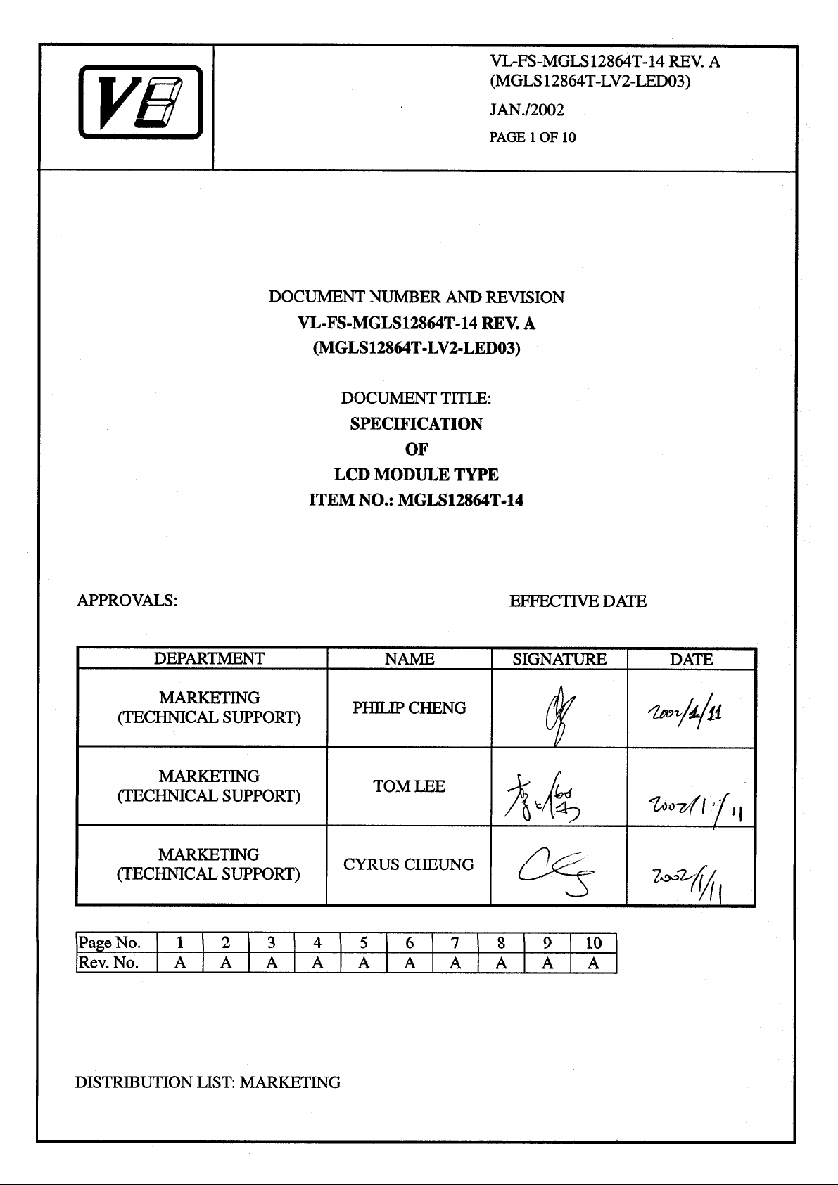
DOCUMENT REVISION HISTORY 1:
DOCUMENT
REVISION
DATE DESCRIPTION CHANGED
BY
CHECKED
BY
FROM TO
A
2002.01.11 First Release
(Based on the test specification
VL-TS-MGLS12864T-14, REV. A,
2001.03.05)
PHILIP
CHENG
TOM LEE
VL-FS-MGLS12864T-14 REV. A
(MGLS12864T-LV2-LED03)
JAN./2002
PAGE 3 OF 10
CONTENTS
Page No.
1. GENERAL DESCRIPTION 4
2. MECHANICAL SPECIFICATIONS 4
3. INTERFACE SIGNALS 6
4. ABSOLUTE MAXIMUM RATINGS 7
4.1
4.2 ENVIRONMENTAL CONDITION 7
5. ELECTRICAL SPECIFICATIONS 8
5.1 TYPICAL ELECTRICAL CHARACTERISTICS 8
5.2 TIMING SPECIFICATIONS 9
5.3 TIMING DIAGRAM OF VDD AGAINST V0 10
ELECTRICAL MAXIMUM RATINGS (Ta=25°C)
7

VL-FS-MGLS12864T-14 REV. A
(MGLS12864T-LV2-LED03)
JAN./2002
PAGE 4 OF 10
VARITRONIX LIMITED
Specification
of
LCD Module Type
Item No.: MGLS12864T-14
1. General Description
• 128 x 64 dot matrix STN LV2 positive yellow transflective dot matrix LCD graphic module.
• Viewing direction: 6 o’clock.
• Driving scheme: 1/64 multiplexed drive, 1/9 bias.
• ‘Toshiba’ T6963C flat pack or equivalent dot matrix LCD controller.
• ‘Toshiba’ T6A39 flat pack or equivalent dot matrix liquid crystal graphic display column drivers.
• ‘Toshiba’ T6A40 flat pack or equivalent dot matrix liquid crystal graphic display row driver.
• 8K byte display SRAM.
• Yellow-green LED03 backlight.
2. Mechanical Specifications
The mechanical detail is shown in Fig. 1 and summarized in Table 1 below.
Table 1
Parameter Specifications Unit
Outline dimensions 78.0(W) x 70.0(H) x 13.0 MAX.(D) mm
Display format 128(Horizontal) x 64(Vertical) dots
Effective viewing area 62.0(W) x 44.0(H) mm
Active area 56.27(W) x 38.35(H) mm
Dot size 0.39(W) x 0.55(H) mm
Dot spacing 0.05(W) x 0.05(H) mm
Dot pitch 0.44(W) x 0.60(H) mm
Weight: TBD grams

VL-FS-MGLS12864T-14 REV. A
(MGLS12864T-LV2-LED03)
JAN./2002
PAGE 5 OF 10
Figure 1: Specification Drawing

P
VL-FS-MGLS12864T-14 REV. A
(MGLS12864T-LV2-LED03)
JAN./2002
PAGE 6 OF 10
3. Interface signals
Table 2
in No. Symbol Description
1 FG Frame ground (see note 1).
2 VSS Ground (0V).
3 VDD Power supply for logic (+5V).
4 V0 Power supply for LCD drive
5 /WR Data Write. Write data into T6963C when /WR=“Low”.
6 /RD Data Read. Read data from T6963C when /RD=“Low”.
7 /CE Chip enable for T6963C.
/CE must be “Low” when CPU communicates with T6963C.
8 C / D /WR = “Low” …..C/D=”High”: Command Write C/D=”Low”: Data Write.
/RD = “Low” ….. C/D=”High”: Status Read C/D=”Low”: Data Read.
9 /RST “High”: Normal (T6963C has internal pull-up resistor).
“Low”: Initialize T6963C. Text and graphic have addresses and text and graphic
area settings are retained.
10 DB0 Data input/output (LSB).
11 DB1 Data input/output.
12 DB2 Data input/output.
13 DB3 Data input/output.
14 DB4 Data input/output.
15 DB5 Data input/output.
16 DB6 Data input/output.
17 DB7 Data input/output (MSB).
18 FS Font select.
“High” for 6 x 8 font &
“Low” for 8 x 8 font.
- A Anode of backlight
- K Cathode of backlight
Note 1: This pin is electrically connected to the metal bezel (frame).
User can choose to connect this pin to VSS or leave it open.

A
H
V
H
VL-FS-MGLS12864T-14 REV. A
(MGLS12864T-LV2-LED03)
JAN./2002
PAGE 7 OF 10
4. Absolute Maximum Ratings
4.1 Electrical Maximum Ratings(Ta = 25 ºC)
Table 3
Parameter Symbol Min. Max. Unit
Supply voltage (Logic & LCD) VDD - VSS -0.3 +7.0 V
Supply voltage (LCD drive)
(Built-in)
VLCD
=VDD – V0
-0.3 +30.0 V
Input voltage Vin -0.3 VDD+0.3 V
Note:
The modules may be destroyed if they are used beyond the absolute maximum ratings.
All voltage values are referenced to VSS = 0V.
4.2 Environmental Condition
Item
Operating
Temperature
(Topr)
Min. Max. Min. Max.
mbient Temperature
umidity
0°C +50°C -10°C +60°C
95% max. RH for Ta ≤ 40°C
< 95% RH for Ta > 40°C
ibration (IEC 68-2-6)
cells must be mounted
on a suitable connector
Shock (IEC 68-2-27)
alf-sine pulse shape
Frequency: 10 ∼ 55 Hz
Amplitude: 0.75 mm
Duration: 20 cycles in each direction.
Pulse duration : 11 ms
Peak acceleration: 981 m/s2 = 100g
Number of shocks : 3 shocks in 3
mutually perpendicular axes.
Table 4
Temperature
Storage
(Tstg)
Remark
Dry
no condensation
3 directions
3 directions

VL-FS-MGLS12864T-14 REV. A
(MGLS12864T-LV2-LED03)
JAN./2002
PAGE 8 OF 10
5. Electrical Specifications
5.1 Typical Electrical Characteristics
At Ta = 25 °C, VDD = +5V±5%, VSS=0V.
Table 5
Parameter Symbol Conditions Min. Typ. Max. Unit
Supply voltage
VDD -VSS 4.75 5.00 5.25 V
(Logic & LCD)
Supply voltage (LCD) VLCD
VDD = 5V, Note 1 9.7 10.2 10.7 V
=VDD –V0
Input signal voltage VIH “H” level VDD-2.2 - VDD V
V
Supply current
(Logic & LCD)
Supply current (LCD) I0 Checker board mode,
“L” level 0 - 0.8 V
IL
IDD Checker board mode,
- 6.38 10 mA
VDD = 5V, Note 1
- 2.24 4 mA
VDD = 5V, Note 1
Supply voltage of
Yellow-green LED03
backlight
VLED Forward current
=100mA
3.9 4.1 4.3 V
Number of LED dies
=20.
Note (1):
There is tolerance in optimum LCD driving voltage during production and it will be within
the specified range.

VL-FS-MGLS12864T-14 REV. A
(MGLS12864T-LV2-LED03)
JAN./2002
PAGE 9 OF 10
5.2 Timing Specifications
At Ta = 0°C To +50°C, VDD = 5V±5%,VSS=0V
Refer to Fig. 2, the bus timing diagram.
Table 6
Parameter Symbol Min. Max. Unit
C/D Set-up time
C/D Hold Time
/CE,/RD,/WR Pulse
t
CDS
t
CDH
tCE, tRD, tWR
100 - ns
10 - ns
80 - ns
Width
Data Set-up Time
Data Hold Time
Access Time
Output Hold Time
tDS
tDH
t
ACC
tOH
80 - ns
40 - ns
- 150 ns
10 50 ns
C/D
/CE
/RD, /WR
Figure 2: Bus Timing Diagram

VL-FS-MGLS12864T-14 REV. A
(MGLS12864T-LV2-LED03)
JAN./2002
PAGE 10 OF 10
5.3 Timing Diagram of VDD against V0.
Power on sequence shall meet the requirement of Figure 3, the timing diagram of VDD against V0.
VDD
95%
LOGIC SUPPLY
VOLTAGE
0V
OV
LCD SUPPLY
VOLTAGE
50ms(typical)
Figure 3: Timing diagram of VDD against V0.
“Varitronix Limited reserves the right to change this specification.”
FAX:(852) 2343-9555.
- END -
V0
 Loading...