

Page 1

Valent F(x) Logi Family
By Andy Gikling (asgikling@gmail.com)
v1.0 - 6/1/2013
A brief beginner’s guide to the Mark 1 FPGA platform
Page 2

Table of Contents
1. Forward ............................................................................................................................................................................ 1
2. Background ...................................................................................................................................................................... 1
3. Getting Started .................................................................................................................................................................. 2
3.1. Running a Pre-Compiled Design on the Mark 1 ........................................................................................................ 3
4. Developing Your Own Design ......................................................................................................................................... 4
4.1. Setup Your Development Environment ..................................................................................................................... 5
4.2. Create Your First Project ........................................................................................................................................... 6
4.3. Add Some Logic to Your Project ............................................................................................................................... 7
4.4. So What Does This Simple Program Do? ................................................................................................................ 10
4.5. Constraining the Design ........................................................................................................................................... 11
4.6. Build Your Project ................................................................................................................................................... 13
4.6.1. Errors! ................................................................................................................................................................ 15
5. Run Your Project ............................................................................................................................................................ 15
6. Where to Go From Here ................................................................................................................................................. 16
6.1. Integrating the Mark 1 with a Host .......................................................................................................................... 16
6.2. Integrate a PMod Device ......................................................................................................................................... 16
6.3. Read Pong P. Chu’s Book ........................................................................................................................................ 16
7. Conclusion ...................................................................................................................................................................... 16
Page 3

1. Forward
This tutorial is designed for beginners interested in getting started working with FPGA technology. FPGAs offer a very new and
robust way to tackle digital system design. Unfortunately, their power and flexibility, coupled with their multidisciplinary nature,
make them extremely complicated to work with. Consequently, the ba rrier to entry is quite a bit higher than your everyday
microcontroller or discrete integrated circuit. An FPGA designer really needs to know a lot of information to make an FPGA do
anything at all.
In an effort to ease this FPGA learning curve and get exposure to a wider audience of electronics practitioners, both hobbyist and
professional alike, ValentF(X) has developed the Mark 1 FPGA board. It is a part of the Logi family of boards and is a fantastic
platform to start out on for anyone who wants to learn about FPGA technology. It has many features that make it easy for beginners to
dive quickly into FPGA development as well as IO capabilities and a form factor that a seasoned professional can even appreciate.
The primary goal of this guide is to take an absolute beginner fro m having a lifeless piece of hardware in fro nt of them, to ma king it
actually do something in a matter of hours. Therefo re, the guide has also been designed to be a concise, goal oriented read. In areas
where verbosity would slow the pace, there are many links to external content provided so you can explore and further your ed ucation
on your own time.
Note, the part of this guide that actually takes the longest is downloading the FPGA development envir onment from Xilinx – the file is
nearly eight gigabytes. If you’re interested in completing this tutorial in an afternoon, start by getti ng the download going now! See
the section called Setup Your Deve lopment Envi ronment
to start downloading the Xilinx “ISE” development software.
2. Background
Field programmable gate arrays (FPGAs) are unique integrated c ircuits (ICs) whose defining characteristic i s that their internal logic
can be reprogrammed indefinitely. They arrived on the scene around 1986 and have grown ever more sophisticated and capable over
the years. Today they are found it many electronics devices such as networking equipment, electromechanical control equipment,
cellular equipment as well as in simpler desi gns such as your car o r maybe even your microwa ve .
At a fundamental level, the “program” running on an FPGA is actually a digital circuit whose wires are “executing” combinatorial
and/or sequential logi c. In FPGAs, the circuits consist of se ver a l to many millions of fundamental logic gates such as an OR, AND,
NOT and XOR gate, just to name a few. An FPGA design typically has man y inpu ts a nd outputs as well as clock s ignals to keep
things synchronized.
It’s really best to think a bout the logic on the FPGA’s “fabric” as a physical circuit. In computing applications that run on processors,
people are normally accustomed to thinking about their program as running in a sequential manner. The code executes from top to
bottoms right? Well, in FPGAs this is t ypically not the case. Everything is ha ppening at once. There can be many parallel “logical
flows” executing at the same time. Furthermore, parallel logical flows can intera c t with each other. In reality, you’re building a
circuit on the FPGA fabric, not a sequential processor. And, as in any circuit you are free to route any wire or “net
destination.
The reprogrammable internal logic found in FPGAs is an immensely powerful feature for many other reasons as well. For example,
back in the days before FPGAs if you were designing a printed circuit board
of course, if a mistake was made in the routing of the elec trical signals you will have nearly irreversible problems.
Say some data signal from pin P73 of component U8 was wired to pin P27 of component U15 on the PCB; you would lay a copper
trace on the PCB and then you are committed to that signal. If there was a mistake made on this trace or for some reason, after the
PCB was manufactured the design no longer needed that signal, you have no option but to revise the board design and manufacture the
board again. With an FPGA you might no t need to do thi s depending on the circumstances. Component U8 and U15 might actually
be in the FPGA fabric and therefor, all you would need to do is reprogram the FPGA to fix your mistake. Also, with an FPGA you
could potentiall y add more functionality to the board’s design after the PCB was made just by reprogramming the FPGA fabr i c !
At a higher level the reprogrammable, digital circuitry found in FPGAs allows designers to put much of the logic found in many
discrete integrated circuits, onto one FPGA chip. This “part consolidation” feature makes for cheaper PCB designs and allows a
greater margin of error in a PCB manufacturing. Imagine a PCB with 30, discrete integrated circuits on it. There would be a very
large number of traces that need to be perfectly placed in order for the design to work. If you took the same design and consolidated
the logic of 25 of these discrete integrated circuits onto the FPGA’s fabric, the PCB would have far fewer traces that could go wrong.
(PCB), the final design is what you were stuck with. And
,” to any
Furthermore, because the FPGA’s internal logic is reprogrammable; the FPGA designers c a n iter a te their logical implementation of
the 25 ICs as many times as they want wit hout incurring any costs of “spinnin g” a new PCB – the only cost is the programmer’s time.
Also, designs based on FPGAs often have a much shorter time to market than a similar ASIC
effective for smaller runs of complex custom hardware.
design and therefore are far more cost
Page| 1
Page 4
Indeed, the current t rend in the electronics industry is moving toward more and more the part consolidation on circuit boards. This
new breed of IC technology has been driven primarily by the mobile computing markets where size and power consumption are of
primary importance. This has given rise to the concept of a system on a chip
FPGA companies, Xilinx and Altera, offer sophisticated tools (Vivado and Qsys respectively) to help a designer efficiently make
FPGAs into effective, reprogrammable SoCs.
The FPGA space is still quite new and the technology is evolving rapidly. Today we find FPGAs with ARM microprocessors in them
which opens up a whole new world of possibilities. Most of all, FPGAs offer a unique and efficient way of sol ving very complex
digital system design proble ms in a n ef ficient, cost-effective manner. So why don’t we dive in!
(or SoC) integrated circuit. For tuna te l y, the t wo maj o r
3. Getting Started
After taking the Mark 1 out of the box, ta ke a moment to look carefully at the unit. You will see the board’s dominant chip is a Xilinx
Spartan 6 FPGA. This is a relatively low cost and high performance device.
Your average electronics consumer will also spot two micro USB headers, some buttons, switches and a bank of small LEDs. A more
trained eye will see two SATA headers, a JTAG interface and even a small square microcontroller by NPX Semiconductor.
You will notice a number of other headers on the board. The ones on top facing up arranged in a straight line can be used for general
purpose IO. The ones facing to the left, bent off the board at a right angle, are Pmod interfaces. Obviously, these bring huge device
expandability to the Mark 1. The headers facing down are designed to fit into a host microcontroller or microcomputer platform such
BeagleBone, Arduino and even the Raspberry Pi! Integrating with these hosts significantly increases the overall system’s
as the
capabilities. Sorry, using the Mark 1 to expand the functionality of one of these popular computing platforms is outside the scope of
this document. There are so many possibilities this topic m e rits its own set of manuals!
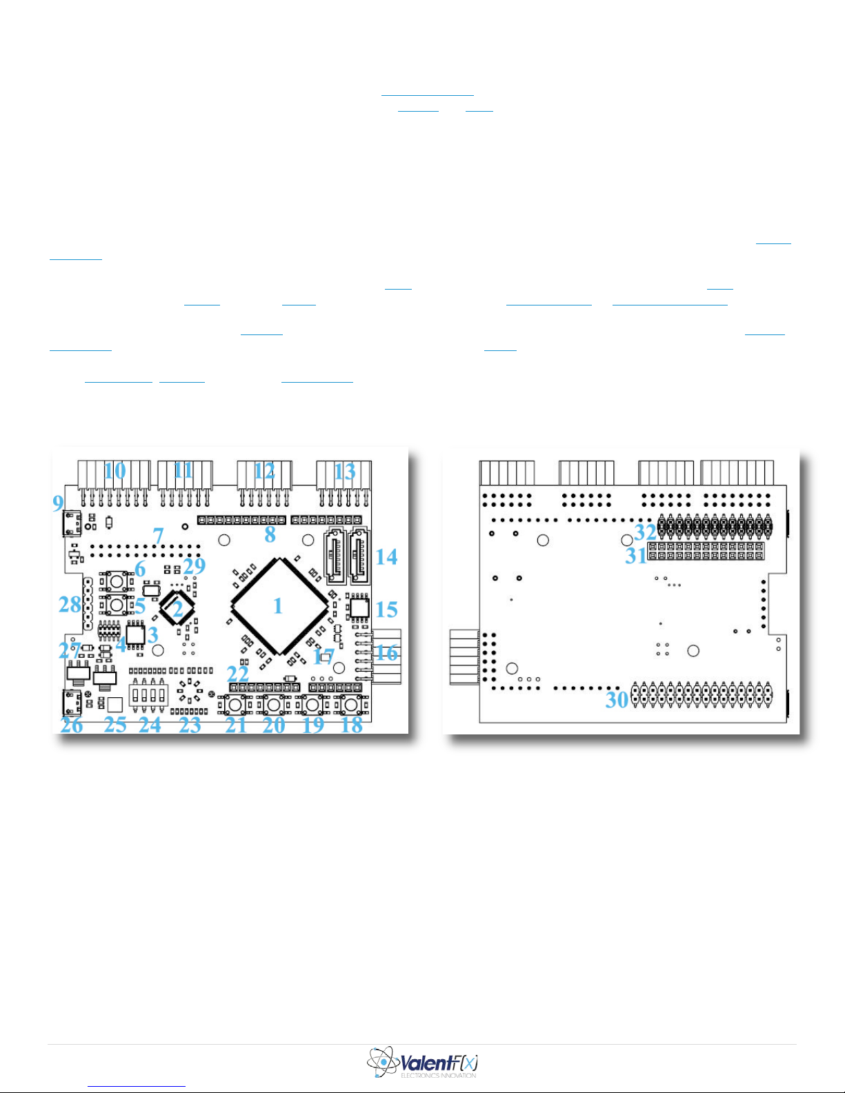
Here is a useful component map of the device:
Figure 1 – Mark 1 Top and Bottom Component Map
1. U5 - Xilinx Spartan 6 - FPGA (XC6SLX9-3TQG144C)
2. U9 - NP X Semiconduct or - Arm Cortex M3 Microcontroller (LPC1343FBD48)
3. U6 - Micron Technology Inc. - 16Mbit Serial Flash (M25PE16)
4. Spare Serial Wire JTAG Header
5. Push Button PB5
6. Push Button PB6
7. P6 Host Connector
8. P1D Arduino Uno Header
9. J11 Micro USB Connector 2
10. PMOD1 Header
11. PMOD2 Header
12. PMOD3 Header
13. PMOD4 Header
14. SATA Headers 1 and 2
15. U10 - Micron Technology Inc. - 16Mbit Serial Flash (M25PE16)
16. PMOD6 Header
Page| 2
Page 5

17. U4 - Abracon Corporation - 50MHz Oscillator (ASDMB-50.000MHZ-LC-T)
18. Push Butto n PB0
19. Push Butto n PB1
20. Push Button PB2
21. Push Butto n PB3
22. P1C Arduino Uno Header
23. LEDs - LED0 through LED7
24. Switches - SW0 thr ough SW4
25. U1 - Future Technology Devices International Ltd. - FTDI UART to USB (FT231XQ-R)
26. J1 Micro USB Connector 1
27. Power Regulation Circuitry
28. J7 - JTAG Header
29. LEDs DC17 and DC18 - power and configuration stat us
30. P28 Header - BeagleBone IO
31. P6 Header - Raspberry Pi IO
32. P29 Header – BeagleBone IO
3.1. Running a Pre-Compiled Design on the Mark 1
The Mark 1 ships with a great “LED counter” demo design that has already been compiled for you. If you’re interested in getting
your hands dirty right away, you can run this program right out of the box! Otherwise, skip down to Developing Your Own Design to
get started making your own FPGA design.
One difficulty with FPGAs is that thei r program or “configuration” is stored in a “volatile memory.” After the FPGA loses its power
it also loses the p rogram it was running. Some FPGAs can store their configuration in non-volatile memory in order to restore their
program automatically on power up without any support circuitry. However, these devices are normally called complex
programmable logic devices (or CPLDs). CPLDs differ in several other ways from FGPAs and are designed to do different things
than FPGAs. Fundamentally both are programmable logic devices.
The Mark 1 has a support microcontroller by NPX Semiconductor on it. This IC is used to configure the FPGA after power up. Using
a microcontroller to assist in the configuration of the FPGA is one of the Mark 1’s best features. With this to pology, the user can
“drag and drop” a program onto the device. The device can then be rebooted by power cycling or pressing the PB5, Reset button.
Then, on system reset, the NPX microcontroller’s firmware
FPGA. In this way, the NPX microcontroller makes “configuring” the FPGA very easy for the end user. If this topology wasn’t used,
the user would need to purchase and extra programmer device to configure the FGPA after power up. This might , for example b e a
programmer connected to the board’s JTAG header. This procedure is much more tedious and would need to be performed every time
the FPGA powers on.
Steps to set the Mark 1’s boot confi guration file usi ng the Windows “drag and drop” method:
1. Usin g a micro USB to standard USB cable, plug the Mark 1 into your Windows
header.
will load the program the use r downloaded to it, onto the Spartain 6
based computer using the J11 mini USB
Figure 2 – Micro USB Connection on J11
Page| 3
Page 6

2. The board will come alive and you will see little green LEDs glowing on it. After a few seconds you will see LED DC17
start flashing if the board already has a configuration file setup on it. This means the NPX microcontroller is configuring the
FPGA. Once the configuration is done you will see DC17 stop flashing and change to sol id green. This means the FPGA is
configured and running its progra m.
3. Once the Mar k 1 is c onnected to your computer Windows wi ll try to install the appropriate device driver. This should
succeed without any issues. When it does, you will see a new Removable Disk in Windows Explorer as shown in Figure 3 .
Figure 3 – New Device Appears in Windows Explorer
4. On the removable disk you will see pre-compiled programs that come saved on the Mark 1’s non-volatile memory.
Figure 4 – Files Factory Preloaded Onto the Mark 1 Board as Shown in Windows Explo r er
5. The file “config.bit” is the file the NPX microcontrolle r is looking for to load onto the FPGA at boot time.
“Config.bit.original” is a backup of the demo program shipped with the Mark 1.
6. To make the s ystem load a totally different FPGA configuration on boot up, simply delete the “config.bit” file and replace it
with a .bit file of your choosing. Just make sure the file that is used for a replacement is named “config.bit.” It’s as simple as
that. No special programmer hardware needed. Later in this guide we will show you how to make the Xil inx ISE generate a
.bit file from your custom design.
7. But, for demonstration purposes let’s have the FPGA run a more interesting program. After deleting the “config.bit” file that
is shipped with the board, use Windows Explorer to make a new copy of “led_counter_i2c_buffered.bit.” If you’re using
Windows 7, highlighting the file and doing a Copy, Paste will generate a copy of the file called “led_counter_i2c_buffered Copy.bit.” Make a copy of the file before renaming it in the interest of pre se r ving this example design for later use.
8. Now rename “led_counter_i2c_buffered - Copy.bit.” to “config.bit.”
9. The final step is to reset the board – just push button PB5.
On system re set you will see the NPX microco ntroller start configuring the FPGA with the config.bit file you just chose. Once it’s
done configuring, you will immediately see LEDs 0 through 7 on the edge of the board start dancing wildly. Each LED represents a
. Because there are 8 LEDs total these LEDs can display 256 unique combinations. What they are actually doing is a very rapid
bit
binary cou nt ing sequence from 0 to 255 in about three seconds. When the sequence finishes it just starts over. Note that the least
significant bit is LED 0 and the most significant bit is LED 7 .
This demo is a very simple example of what’s possible on this FPGA platform. With a little more learning and HDL code
development, you can be on your way to blinking lights in your own sequence in no time! …Or reading MP3s off your SATA
connected, terabyte hard drive while playing the audio and displaying a visualizer! …For example.
4. Developing Your Own Design
Now that you have a bit of FPG A background we will move on to the hands-on part of this instructio n. In the following sections you
will learn what is required to actually d e sign and build your own FPGA configurati on and then run it on the hardware. The example
design given below is ra ther simple, but seeing the major FPGA software development concepts and workflo ws that are exposed
through this tutorial will be instrumental in understanding the big picture.
Page| 4
Page 7

4.1. Setup Your Development Environment
Software development for the Spartan 6 target is d one in Xilinx’s ISE development environment (ISE loosely means Integrated
Software Environment). As of this writing, Xilinx is on ISE version 14.5. Go here to start downloading it. If you have a slow or
unreliable, connection you might want to download the file in parts. I f you have a fast broadband connection, shoot the moon and go
for the full DVD single file download – the full download can be found about half way down the page linked to above and it’s 7.79GB
– so get started. (Also note you want to install the Xilinx ISE for this tutorial, not Vivado which is Xilinx’s SoC design tool.)
When the file is finally done downloading you will need to extract its contents to your hard drive as your download comes in a .tar
archive format (That is, if yo u’ve downloaded the entire DVD in one file. Otherwise, follow the instruction on the website for ho w to
reassemble a multi-part download). If you’ve never used .tar archives there is a pleasant little open source program you should have a
look at, 7Zip
“xsetup.exe” under the extracted files’ root folder. Run this installer program and follow the on screen instructions. A “typical”
installation will suffice. This rather long document is the official
installation.
When the installation completes, open the Xilinx ISE (you wil l most likely find it in your Start menu’s A ll Programs list under “Xilinx
Design Tools > ISE Design Suite 14.5 > ISE Design Tools > 32-bit Project Navigator”). The ISE download comes with the “full”
version of the software. However, your computer will not have licenses to enable the various features Xilinx offers. Therefore, you
need to get your own license file before you continuing.
. It’s archiving software you can use to extract the files. Once you’ve extracted the contents of the .tar file you will see
Xilinx Install Guide. Consult it if yo u have probl ems with the IS E
Go to the Xilinx website
what you will find is your user account gives you access to many useful design resources. With a Xilinx user account you can watch
training videos, use the forum, get updates and add-on software, and get license files – it’s totally worth it.
Xilinx offers many different licensing tiers. We will be using the free “WebPack” license. This enables enough software features to
get us started. The WebPack allows your software to compile and you can use most of the basic Xilinx development tools.
In the ISE, navigate to the “Help” toolbar on the top of the screen and choose “Manage License.” This opens the Xilinx License
Configurati on Manager . Under the “Acquire License” tab, select the “Get Free ISE WebPack License” radio button and click Next:
and create a user account. Yes, needing a user account might seem like overkill if you’re a beginner, but
Figure 5 – Xilinx License Configurat ion Manager
The software will gather s ome unique information about your machine and then give you the option to “Con nect N ow.” Click it:
Page| 5
Page 8

Figure 6 – Unique Computer Info Tied to WebPack License
At this point the software will ope n your web browser and bring you to the Xilinx site. It will ask you to login with your user account.
Do it and follow the on screen instructions. Once you complete the on screen steps Xilinx will email you a license file with the file
extension .lic. Save this .lic attachment somewhere safe. The ISE installation directory would suffice. The email also contains
instructions on how to install the lice nse.
Essentially all you need to do is open the Xilinx License Configuration Ma nager again, click the Manage Xilinx Licenses tab, and
click Copy License. This will open a dialog that lets you find and select the .lic license file you d ownloaded from your email. Select
it and click Ok. Under the Manage Xilinx Licenses tab the table should now be populated with details about what features of the
software are enabled by your WebPack license. Congratulations, your software is setup and ready to go!
4.2. Create Your First Project
In this tutorial we will be using the Mark 1 hardware to create a working Verilog HDL design. We will keep the physical goals simple
in order to demonstrate the basics. In the following example, the Mark 1’s buttons will be used to turn on some of its LEDs.
Thrilling! Absolute l y ye s, but it’s an invaluable exercise none the less. Let’s begin with creating our “Project” file in the ISE Project
Navigator.
In the Xilinx ISE, like many other engineering progra ms, us e r s create “Projects” to save all aspects of their design. FPGA designs
often consist of many files of many different file types. The Project encapsulates everything and serves as a means to easily manage
all the FPGA’s design files. (ISE Project files contain references to many support files like the source code files and configuration
files. They have a .xise file type.).
To create a project for this tutorial, open the Xilinx ISE Project Navigator. Under the File menu, choose New Project… you should
see the New Project Wizard open. Choose some file paths and a name for your project (it is recommended each of your projects be
put in its own folder to c ontain all the design files in one place):
Figure 7 – The New Project Wizard
Page| 6
Page 9

After clicking next you will find the project’s settings page. You can use the settings shown below for the Mark 1 board. These
settings can be changed at any time later on. This wizard page is designed to let you choose important software environment settings
from lists of possibilities.
For example, it is on this dialog where you specify what chip you’re de s igning for, the speed gr ade, and physical package. You also
set which software toolchain
shortly.
and HDL language you prefer. We’ll touch on what the common tools are and why they are used
Figure 8 – Project Settings
The last page is a summary of your chosen settings displayed in plain text. Click Finish and you will be brought into the ISE Proj ect
Navigator development environment. You are now ready to add content to your design.
4.3. Add Some Logic to Your Project
Take some time to look around the software. The Project Navigator has a clean looking layout and there can be an enormous density
of information displayed at once. Windows users will be familiar with the standard set of menu items located across the top of the
screen; File, Edit, View, Project, Source, Process, Tools, Window, Layout and Help all contain items that f it their respective
categories – as is tradition. The rearrangeable butto ns across the top are concise and self-explanatory as well.
In the default workspace view, the top left pane shows the Project’s “Hierarchy.” This tree view shows the relationship between
various HDL modules in t he design. You can use this pane to add or remove HDL files from the project.
FPGA are often designed in a tree structure of “modules.” Modules are blocks of logic that encapsulate
a design. The blue link describes encapsulation in the context of object-oriented programming but really the term is effective in a
broader sense; HDL modules are can be thought of as “layers” that encapsulate the logic of some abstract but compartmentalized piece
of circuitry. The “top level” module is the “root” of the tree of HDL modules. Although this design will not provide an example of
how to add sub modules to the tree hierarchy, be aware that this is easily done and very common.
some discrete, unique part of
Let’s start by adding your design’s to p level HDL file.
Page| 7
Page 10

Figure 9 – An Empty Design in the Hierarchy View
To add a top level HDL file, right click the target chip i n the Hierarchy view (denoted by the model, xc6slx9…) and choose New
Source. This will bring up a view that allows you to add a design file to your project. There are many different types of files you can
choose here but for this i nstruction we will have you load a new “Verilog Module.” Give it a name and click Next.
Figure 10 – New Source Wizard
On clicking next you are presented with a GUI that lets you defi ne the module’s input and outputs. It ’s convenient to think of Verilog
HDL modules as chips on a circuit board. T ypically a chip has a number of pins that are either inputs or outputs. This GUI lets the
user specify names for the module’s IO, then, when the Verilog HDL file is generated and added to the project it will contain
definitions for these IOs. Setup your Verilog module like t he picture below. Note that you don’t need to specify these IO points as
being “buses” or what their most or lea st sig nificant bit is – all of these IO points are just one bit (or wire - depending on how you
view the worl d).
Page| 8
Page 11

Figure 11 – A Top-Level Verilog Module’s IO Definition
In the Hierarchy view you will see a new Verilog source file called “Mark1Starter_TopLevel.v.” “.v” is the file extension for Verilog
files. Double click it and its content s will be shown in the text editor on the pane to the right. Here is what you should see:
Figure 12 – An Auto Generated Ver i log Module
You will notice that the Verilog syntax is highlighted. Things marked in green are comments, blue are Verilog language keywords
and the pink at the top used to denote the module’s timing information for simulating the design (we’re not going to touch on de s ign
simulation).
At this point you have your top-level Verilog module defined and all you need to do is add logic to it. The module takes in two bits
and can output two bits. One could even think of these as wires coming in and goi ng out of our module. We will use the
“OSC_FPGA” input bit to d e fine a system clock signal. This signal will be used to turn over the logic on a specific time base.
Page| 9
Page 12
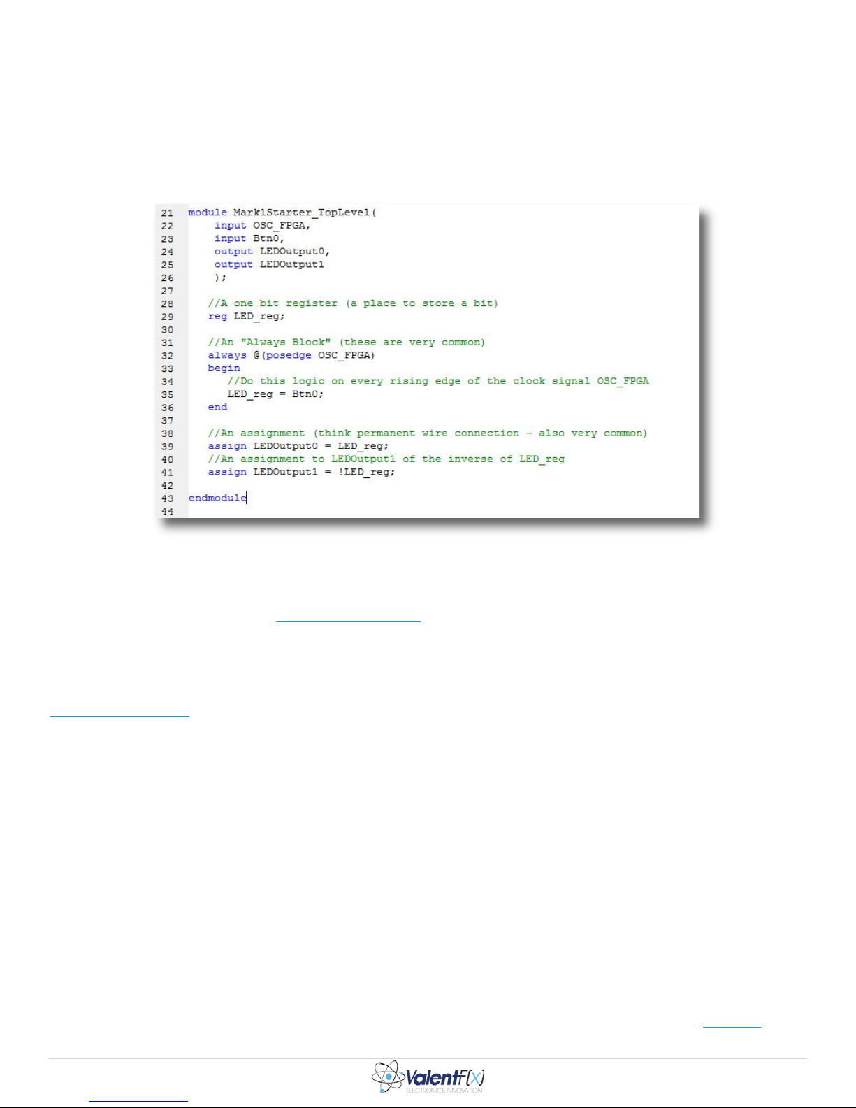
The “Bt n 0” input represents the wire coming from PushButton0 on the PCB. Similarly, “LEDOutput0” and “LEDOutput1” represent
the wires going out to LED0 and LED1 on the PCB.
What we’re going to do with these signals is ground breaking… The goal is when the button is not pushed, LED0 will be illuminated
and LED1 will not be illuminated. Then just whe n yo u lea s t exp e c t it, Btn0 will be pushed and the LEDs will flip -flop states; LED0
will become dark and LED1 will illuminate. Like I sa id, ground breaking stuff!
Although this truly novel goal can be accomplished without a clock signal we will implement the solution using a system clock. Add
a few lines of code to your design as shown below:
Figure 13 – Verilog HDL Code for Example Design
4.4. So What Does This Simple Program Do?
The goal of this document is to get the user on their feet, not to teach Verilog HDL sorry... If you are really interested in learning
Verilog see the section at the end called Where To Go From Here.
In the module’s definiti on we have two inputs and two outputs. For now, assume the Btn0 input is exter nally wired to the user
PushButton0 on the PCB and OSC_FPGA is connected to our clock source – these are t he inputs to the module. Also assume
LEDOutput0 and LEDOutput1 are connected to LED0 and LED1 on the bank of LED s – these are the outputs. These external
connections to hardware IO are defined in the design’s “user constraints” file. Constraining a design is described below in the section
Constraining the Desig n.
Just below the module’s definition ( line 2 9) we’ve defined a “register” that is one bit “wide” called LED_reg (registers like this can be
defined as multi-bit registers if desired). This register can store the state of one bit of data and it is used as such.
After the register definition there is an “Always Block” (line 32). Verilog structures like this Always Block are a common way to
define synchronous clocked circuitry. Wha t this block describes is on every rising edge of the input clock signal, OSC _FPGA, the
status of the Btn0 bit will be set to the o ne bit register LED_reg. OSC_FPG A is oscillating at 50MHz so the logic between the Begin
and End in thi s Always Block is being “executed” fifty million times per se cond.
On the bottom we have two “Assign” statements. The simplest way to describe Assign statements is to think of them as wires being
connected together permanently. The logic is not dependent on a clock. As soon as LED_reg’s value changes because of the Always
Block above, the value immediately propagates to the output wires LEDOutput0 and LEDOutput1. Notice that LEDOutput1 is getting
assigned the inverse state of LED_reg. T he exclamation point operator denotes a logical NOT gate (as in many other computer
languages).
That said here is a quick description of what’s going on.
Remember, Verilog is a hardware description language. The logic in this module can be imagined as an actual circuit that does
exactly what is described.
When executi on starts, LE D0 will be on and LED1 will be off. This might be counter intuitive but there are two important things that
cause this initial condition. First, the user PushButton0 input, Btn0, is electrically connected as negative logic (aka “active low
when the button is pressed the wire changes to false, or zero volts. So under normal circumstances, when the button is not pressed this
” –
Page| 10
Page 13

IO point is true). And second, the LEDs on the PCB are electrically connected in a positive logic manner (or “active high” – when the
LEDOuput0 changes to true, a positive voltage is put on the output pin and current will fl ow through the LED and illuminate it).
For these reasons, the initial cond ition for this circuit has LED0 on and LED1 off when PushButton0 is not pressed. When the
module’s input wire, Btn0, changes from true to false because the user pressed PushButton0 on the PCB, the logic shown above will
assign this false input to our LED_reg register on the rising edge of the next OSC_FPGA c l ock signal.
Finally, because the module logic has used an Assign statem ent to assign t he value of LE D_reg to the LEDOutput0 wire and its
inverse to LE DOutput1, you wil l the n see LED0 go dark and LED1 illuminate on the PCB when PushButton0 is pr essed.
For more det ails on how the surrounding hardware is connecte d to the FPGA consult the Mark 1 electrical schematic
below is the electrical drawing that details the FPGA’s outputs to the bank of LEDs (found on page 5 of the schematic). Clearly, when
the L7 output changes to a logic high level, current will flow through the LED 0 to Ground and the LED will illuminate.
Figure 14 – Electrical Drawing of FPGA’s Outputs to Bank of LEDs
To illustrate the inverting nature of our user PushButton0 the following is a drawing of the input circuit (also found on page 5 of the
electrical schematic). You can see that the FPGA’s input, PB0, has a 4.7kOhm “pull-up” resistor attached to it. This means the lo gic
level on this wire is normally connected to 3. 3v which is a logical true. Only when the user presse s the button does this input wire’s
voltage level fall to 0v, or false, because the button connects the wire to Ground.
. For example,
Figure 15 – Electrical Schematic of Active Low Push Button Inputs to FPGA
4.5. Constraining the Design
In the previous section we described a simple module that turns some LEDs on and off based on the state of an input push button. The
Verilog that describes the circuit is simple. It was entirely defined in one top -level module with two inputs and two outputs. What we
didn’t describe is how this simple design links the module’s inputs and outputs to physical IO points on the FPGA.
Page| 11
Page 14

This is where the “Implementation Constrains File” comes in. These files have a .ucf file extension and describe the design’s “user
constraints.” Design constrains are a set of rules the compilation process needs to take into account when building the design’s binary
output file. This “.bit” file is output by the compilation pro c e ss and is the file that gets downloaded and run on the FPGA as described
in the section called Running a Pre-Compiled Des ign on the Mark 1
Some examples of types of things that can be constrained in an FPGA design are:
• Timing const raints
• Logical constraints
• Physical constraints
• Mapping and Routing constraints (or directives)
• Physical pin assignment
User constraint files can vary dramatically in complexity and detail. The topic is very vast and discussing it in detail is outside the
scope of this document.
So there is a huge amount of information to know surrounding how to constrain designs, but fortunately fo r us, our design only needs
to constrain a handful of items to work properly (this design is so simple we’re also not going to worry about enforcing any timing
constraints either). All that we need to do is to define what hardware pins our top-level Verilog HDL module’s inputs and o utp uts link
up to. We also give some details about the design’s clock input, OSC_FPGA.
Start by adding a constraints file to the project. Right click anywhere in the project Hierarchy view and choose New Source. This
time, select Implementation Constraints File, give it a name and choose Next :
.
Figure 16 – Add a new constraints file to the design
A Summary window will appear. Click Finnish. Now in your project Hiera rchy view you will see a new “.ucf” file. Double click it.
The Text Editor view on the right window pane will show your file is totally empty. Add the following code to it then we will discuss
what each piece means:
Figure 17 – Implementation constraints file
Page| 12
Page 15

As is tradition, the green denotes comments and the language syntax are highlighted appropriately. Thank goodness for modern
IDE’s… and remember to end each statement with a semicolon! The 4
parameter gets the name clk50_grp. TNM_NET is a keyword used for defining a design’s clock signals. Again, there are many
keywords that can be used in an infinite number of ways in these constraints files. Don’t worry about the details of this line until you
take the time to actually study more advanced FPGA principles such as Timing Closure
Constraints Guide.
After the OSC_FGPA net declaration is a new TIMESPEC definition (line 7 ) . This constraint essentially calls out how fast our
OSC_FPGA clock signal is. A 20 nanosecond clock period means the clock is r unning at 50MHz. Yo u’re free to research exactly
what this keyword means but for our purposes, you can regard this line as “magic.”
Lines 10 through 13 define some new nets and use the LOC key word to assign them to the FPGA’s physic al pins. Thi s is how we link
our top-level Verilog module’s inputs and outputs to phys ical pins on the IC. The names of these nets must be identical to the names
of your module’s input and output ports! The pin number can be found by referencing the electrical schematic; the following is taken
from page 7:
th
line defines a “net” called OSC_FPGA and its TNM_NET
or consult a recent copy of the official Xilinx
Figure 18– FPGA Bank 2 Electrical Drawing
Here you can see all the connections to Bank 2 of our FPGA. You can see wires connecting the FPGA to all 7 LEDs on the board.
Note that the LED wires are connected to the pin number called out above. Furthermore, you can see the pins’ official name next to
the input. These match what’s written in the comments of the constraint s f ile . This is common practice.
For example our design uses LED0. This LED is connected to pin 41 and that pin’s name is IO_L64P_D8_2. In our constraints file
we can see that we’ve called out the net LEDOutput0 to land on “P41” using the LOC keyword. In the above s chematic you can also
see the FPGA’s clock input on pin 55 and the oscillator IC it’s connected to.
4.6. Build Your Project
We’re almost done! Phew! All that’s left i s to compile the design and then we’re ready to run. If you’ve followed the directions
above carefully this step should be simple!
The final step is for the Xilinx software toolchain to take all of your design files a nd c ompile them into one single “bit-stre am” file, or
“binary” file as it’s often called. With a file type of .bit, this is the file that gets downloaded to the FPGA and run. Remember, at
power up, an FPGA doesn’t have a program loaded onto it. The vast arrays of programmable logic blocks in an FPGA need to receive
a configuration before the chip does anything useful. Once configured, the FPGA starts e xecuting your program.
There are a handful of software build steps that need to be complete for the toolchain to outp ut a b it-stream file. Novels have been
written about each topic but here’s a rapid summary:
1. Synthesize – This step is where the Xilinx XST tool converts HDL logic into a gate-level netlist. This low level netlist is
represented in terms of the UNISIM component library. If your HDL code has syntax errors this step will not complete.
Fortunately, the Output window pane at the bottom of the ISE will tell you where the er ror is.
2. Implementation – This step converts the gate-level netlist into a placed and routed design that fits on the chip selected. This
is composed of three discrete build steps.
Page| 13
Page 16

a. Translate – The NGDBUILD software tool is used to translate the netlist from using the UNISIM library to the
SIMPRIM library.
b. Map – the MAP software tool is used to take the SIMPRIM primitives and decide how the chip’s physical resources
(flip-flops, BRAMs, Multipliers, LUTs etc.) will be used.
c. Place and route – the PAR software program runs a lot of computation to layout where all the chips resources will be
used and how the design com p onents get placed, routed and interconnected.
3. Generate Programming File – The final step takes the output from the previous steps and puts t hem together i nto a single
binary that can be used to program the device.
The ISE Project Navigator has an entire window pane dedicated to this process. This is because when designs get very large these
discrete steps can take hours! An engineer would not like to have to re-run every step of the compilation process if it’s not necessary.
The following view can be used to explicitly run individual steps of the build process and see the status of what’s currently running or
even what’s failed (note in order to see the following view you must have the Mark1Starter_TopLevel.v file selected in the Hierarchy
view:
Figure 19 – The Process View
Simply click the little green pla y button in the top left corner to compile the whole design. On a modern computer this should take
less than 2 mi nutes to run for this project. If the process completes without any errors you will get green check boxes next to the
major steps in the compilation process:
Also you will note the Console view pane on the bottom of the ISE will show output like the following:
Figure 20 – A Successful Build
Page| 14
Page 17

Figure 21 – Console Output at the End of a Successful Build
4.6.1. Errors!
Chances are you’re going to make a mistake at some point along the way. If not in this tutorial, someday, you will make a mistake
and get a compiler error, sorry. In this case one of your build steps will have a red X next to it. The X isn’t entirely helpful to a
beginner. It does tell you which build step failed and to the trained developer this can greatly narrow the scope of what’s gone wrong.
More often t hough you will immediate ly query the e rror log to fi nd out what’s going on.
For example, if you try to recompile your design with an extr a comma in your module defi nition (immediately after LEDOutput1 and
before then module definition’s end parentheses…) the error tab yields this relatively clear message:
Figure 22 – Syntax Error Found During Synthesis
The probl em is indeed on line 26, this is an easy one to find and fix i f you know Verilog.
If you get errors, don’t fret. This is normal. It happens all the time. Read the error message carefully and try to understand what the
compiler isn’t happy about. Non-developers tend to forget this but error messages are designed to point you to the problem so you can
resolve it! Imagine a world without error messages!
You will find that when you’re new to a programming language, working through compiler errors teaches you about what’s allowed
and what’s not allowed slowly, but effectively. However, in general, it’s advisable to save yourself some headache, buy a beginners
book on the langue and power through it before taking on any serious projects.
5. Run Your Project
If you’ve got t en this far i t means you’ve c reated your very own FP GA design in the Xilinx IS E. You’ve added a Verilog HDL
module to the design, constrained it, c ompiled it and now you’re ready to run it!
But before you do, you need to generate the programming “binary” file that gets downloaded to the target. Simply double click the
build step called “Generate Programming File” in the Process view (it’s directly under Place & Route).
When this finishes successfully, open Windows Explorer and navigate to the folder where you’ve saved your project files. In this
folder you will see a .bit file with the same name as your top-level module, “Mark1Starter_TopLevel.bit” in this tutorial ’s c a se.
This bit file can be used to configure the FPGA as described above in the section Running a Pre-Compiled Design on the Mark 1
Essentially you plug your Mark 1 into a USB port on your computer. When the Mark 1 appe ars in the Windows Explorer as a
removable disk, copy and paste the Mark1Starter_TopLevel.bit file onto the removable disk. Once it’s on the removable disk, change
the file’s name to “config.bit.”
.
Page| 15
Page 18

Now power cycle your Mark 1 and see, once the FPGA is configured that, YAY!!!! LED0 i s on!!!! AND when you press
PushButton0, LED0 turns off and LED1 t urns on! Wow super cool!
6. Where to Go From Here
There are many places you can go from here. You’ve successfully programmed an FPGA and now the sky is the limit. Have a look
over the following sections to see what else is possible with the Mark 1 platform.
6.1. Integrating the Mark 1 with a Host
The Mark 1 was designed to be mounted on a number of host circuit boards such as the Beaglebone, the Raspberry Pi, and the
Arduino Uno.
When integrated with these powerful microcomputers and microcontrollers, the Mark 1 platform can do some truly amazing things.
Combining the signal routing and interfacing capabilities of the Mark 1 with a high speed processor allows a design to do many more
things than either component can do on its own.
Here’s a short list of open source projects where a computing platform has been integrated with the Mark 1:
• Bitcoin Miner
o http://valentfx.com/logi-blog/item/fpga-logi-family-bitcoin-mining-application
• Autonomous Vehicle Platform – A design to drive a car through a course. Integrates sensors and the Raspberry Pi
o http://valentfx.com/logi-blog/item/logi-bot-autonomous-vehicle-project-for-logi-boards
• Image Processing Application – Implementation of a Sobel Filter for the Mark 1 and Beaglebone
o http://valentfx.com/logi-blog/item/logi-guide-image-processing-sobel-filter-demo
• Camera Interface Board – A PMOD camera interface board
o http://valentfx.com/logi-blog/item/logi-camera-pmod-pcb
As you can see, clearly the Mark 1’s flexibility and power is highlighted when the device has a ho st p la tform. To be sure, there will
be many more projects like the above to come. If you are a more advanced user you will likely be using a host platform in your des ign
already. ValentF(x) has plans to release an official integration guide with source code for each of these popular microcomputer
platforms. The data link will likely be SP I , GPMC or I2C.
Another advantage integrating the Mark 1 with a microcomputer has is beginners can then see examples of writing software in
languages like C and C++ along with their HDL deve lopment. Furthermore, for anyone working in the electronics or software
industries, having a working knowledge of Linux is certainly worthwhile as well. And these host platforms provide exposure to
embedded Linux! The Mark 1 coupled with a host, is truly great way to study Linux software development and computer science in
general.
– An FPGA based Bitcoin miner design for the Mark 1 and Beaglebone
6.2. Integrate a PMod Device
The PMOD headers on the side of the Mark 1 allow for easy connectivity to “caned” electronics modules. You c an add things like
GPS, Audio Amplifiers, OLED displays, Wifi, Networking, RS232, DACs, ADCs Accelerometers, Moto r D rivers etc. to your design!
Have a look through all the PMOD possibilities at the Digilent site.
6.3. Read Pong P. Chu’s Book
There’s a great intro book by Pong P. Chu that you should read if you want to develop a sound understanding of the Verilog or VHDL
languages. ValentF(X) and open source supporters are porting a number of the exampl es from this book so they can be run right on
the Mark 1 platform.
7. Conclusion
I hope you were able to work through this tutorial at a reasonable pace. I also hope the detail was such that you could grasp t he major
topics surrounding the FPGA development workflow witho ut too muc h hea d ac he. This document will certainly be revised as this
platform evolves. Also stay tuned for a Beaglebone or Raspbery Pi integration guide. Feel free to contact me with questions,
comments or corrections. Good luck and have fun explo ring the world of FPGA design!
Page| 16
 Loading...