

Vaishali Semiconductor VT98001Q, VT98001QX Datasheet
Advance Information
r
VT98001
Multifrequency Synthesize
Applications
•= Set-top boxes •= MPEG Video clock source
General Description
The Vaishali VT98001 is a single-c hip, integr ated multiple Phase Locked Loop (PLL) clock synthesizer. The
device uses an analog Phase Locked Loop (PLL) to accept a 27 MHz crystal input to produce multiple
outputs. Selection pins are used to provide various outputs.
Features
•= 24.576 MHz for Firewire IEEE1394 or video
digitizer
•= 24.576 MHz / 28.224 MHz for software or
hardware modem
•= 27 MHz buffered output clock
•= 6.000MHz buffered output clock
•= 18.432 MHz for audio processor
•= 2kHz standby clock
•= Zero ppm synthesis error in all clocks
(except the 2 kHz standby clock)
•= 5V tolerant inputs
•= 20-pin, 150 mil SSOP (QSOP)
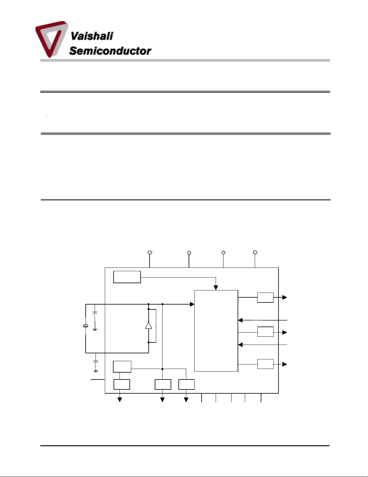
Figure 1. Functional Block Diagram
ROM Table
27 MHz
Crystal
X2
osc
X1
Divider
/PD
VDD2
VDD3 VDD1
VDD4
Buffer
24.576/
28.224 MHz
PLL
Multiplier
BufferBufferBuffer
Buffer
Buffer
Select
24/28 MHz
24.576 MHz
MODE
18.432MHz/
6.000MHz
2kHz
GND1
GND4 27 MHz 27 MHz GND2 GND3
GND5
2001-07-25 Page 1 MDST-0013-00
Vaishali Semic onductor 747 Camden Avenue, Suite C Cam pbel l CA 95008 P h. 408.377.6060 Fax 408.377.6063
www.vaishali.com
VT98001 Advance Information
Figure 2. Pin Configuration
VT98001
Select 24/28MHz
X2
X1
VDD1
VDD2
GND1
GND2
24.576MHz
MODE
24.576MHz/28.224MHz
20
1
2
3
4
5
6
7
8
9
10
GND5
27MHz
19
27MHz
18
VDD4
17
VDD3
16
15
GND4
14
GND3
13
18.432MHz/6.000MHz
12
/PD
2kHz
11
Table 1. Pin Description
Name Pin # Type Description
Select 24/28 MHz 1 I(PU) Select 24.576 MHz or 28.224 MHz output
X2 2 O Crystal connection. Connect to a 27 MHz crystal
X1 3 I Crystal connection. Connect to a 27 MHz crystal
VDD1 4 P Connect to 3.3V
VDD2 5 P Connect to VDD
GND1 6 P Connect to ground
GND2 7 P Connect to ground
24.576 MHz 8 O Clock output, 24.576 MHz
MODE 9 I(PU) Mode control. See Table 2
24.576 MHz/ 28.224MHz 10 O Clock output, 24.576 MHz or 28.224 MHz
2 kHz 11 O Clock output, 2 kHz
(1)
/PD
12 I(PU) Powerdown control. When LOW, all clocks are disabled except
2kHz standby clock
18.432MHz/6.000MHz 13 O Clock output, 18.432 MHz or 6.000 MHz
GND3 14 P Connect to ground
GND4 15 P Connect to ground
VDD3 16 P Connect to VDD
VDD4 17 P Connect to VDD
27 MHz 18,19 O 27 MHz buffered clock outputs
GND5 20 P Connect to ground
Legend: I = Input
O = Output
P = Power supply connection
I(PU) = Input with a 250k ohm pull up
Note (1). All disabled cloc k outputs are tristated (high impedance).
2001-07-25 Page 2 MDST-0013-00
www.vaishali.com
Vaishali Semic onductor 747 Camden Avenue, Suite C Cam pbel l CA 95008 P h. 408.377.6060 Fax 408.377.6063
 Loading...