

Vaishali Semiconductor VT83027S1X, VT83027S1, VT83027-D, VT83027-DW Datasheet
2001-04-17 Page 1 MDST-0003-03
www.vaishali.com
Vaishali Semiconductor 747 Camden Avenue, Suite C Campbell CA 95008 Ph. 408.377.6060 Fax 408.377.6063
Applications
•= Set-top boxes
•= Telecom switching
•= HDTV
•= MPEG Video clock source
General Description
The Vaishali VT83027 is a single-chip, integrated VCXO and Phase Locked Loop (PLL) clock synthesizer.
The device uses the VCXO and an analog Phase-Locked Loop (PLL) to accept a 13.5 MHz, 14 pF (pull
range of 200 ppm) crystal input, and produce a 27 MHz output. A 0 to 3V control signal is used to fine tune
the output clock frequency in the ±100ppm range.
Features
•= 3.3V supply operation
•= Low jitter PLL Clock Synthesizer
−= Zero ppm synthesis error
•= Uses inexpensive pullable crystal
•= ±12mA drive capability
•= On-chip oscillator with 200 ppm pull
range (±100 ppm)
•= 8 pin SOIC package
VT83027
27MHz, 3.3V VCXO
(Voltage-Controlled Crystal Oscillator)
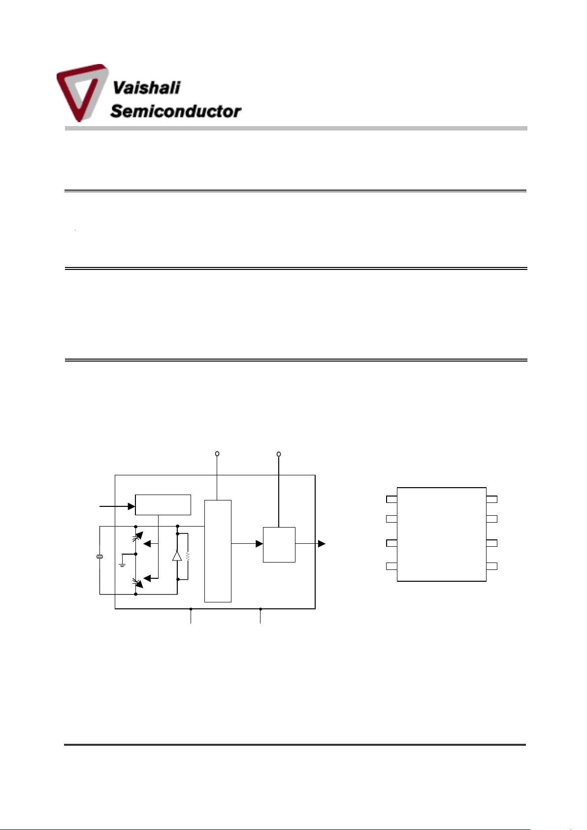
Figure 1. Functional Block Diagram
CLK1
VDD2
X2
Load Cap
Control
Low
Phase
Noise
PLL
Output
Buffer
osc
VDD1
13.5 MHz
Pullable
Crystal
VIN
X1
GND1 GND2
Load
Caps
8 pin (150 mil) SOIC
VT83027
X1 X2
VDD1
VIN
GND2 CLK
1
2
3
4
5
6
7
8
GND1
VDD2
Figure 2. Pin Configuration
VT83027
2001-04-17 Page 2 MDST-0003-03
www.vaishali.com
Vaishali Semiconductor 747 Camden Avenue, Suite C Campbell CA 95008 Ph. 408.377.6060 Fax 408.377.6063
Table 1. Pin Description
Name Pin # Type Description
X1 1 Xi Crystal connection. Connect to a 13.5 MHz pullable crystal
VDD1 2 P Core VDD. Connect to 3.3V
VIN 3 I Voltage input to VCXO. Zero to 3V signal controls the frequency of the
VCXO.
GND2 4 P Connect to ground.
CLK 5 O Clock output
VDD2 6 P Output driver V
DD
. Connect to 3.3V
GND1 7 P Connect to ground.
X2 8 Xi Crystal connection. Connect to a13.5 MHz pullable crystal.
Legend: I = Input
O = Output
P = Power supply connection
Xi = Crystal connections.
Table 2. Pullable Crystal Specifications
Parameter Value
Correlation (load) capacitance 14 pF
C0/C1 240 max
ESR
35 Ω max
Operating Temperature
0°C to +70°C
Initial Accuracy ±20 ppm
Temperature + Aging Stability ±50 ppm
Table 3. Absolute Maximum Ratings
Parameter Conditions Min Typ Max Units
Supply voltage, VDD Referenced to GND 5 V
Inputs and Clock Outputs Referenced to GND -0.5 VDD+0.5 V
Soldering Temperature Max of 10 seconds 260 °C
Storage temperature -65 150 °C
Stresses above those listed under Absolute Maximum Ratings may cause permanent damage to the
device. These ratings are stress specifications only and correct functional operation of the device at these
or any other conditions above those listed in the operational sections of the specifications is not implied.
Exposure to absolute maximum rating conditions for extended periods may affect product reliability.
 Loading...