

Vaishali Semiconductor VS3V257Q, VS3V257QX, VS3V2257QX, VS3V2257Q Datasheet
VS3V257 / VS3V2257
A
A
A
High-speed 3.3V CMOS VSwitch
Quad 2:1 Mux/Demux
Applications
•= 3.3V to 2.5V translation
•= 2.5V to 1.8V translation
•= Hot-Swapping
General Description
The VS3V257 is a high-speed LVTTL–compatible Quad 2:1 multiplexer/demultiplexer. The VS3V257
contains four mux /demux channels, with a com mon path c ontrol (S) and active low enable (/E) . The low ON
resistance of the VS3V257 allows inputs to be connected to outputs , without adding propagation delay and
without generating additional signal noise. The VS3V2257 has 25Ω resistors in series with the switches to
reduce ground-bounce noise and signal reflection.
The VS3V257 and VS3V2257 are designed for 3.3V to 2.5V or 2.5V to 1.8V level trans lation, without any
external components. These switches also offer very high impedance between switch terminals in the
power-off or “disabled” state. This feature, combined with near-zero propagation delay in the “on” state,
makes VS3V257 and VS3V2257 ideal interface elements for hot-swapping applications.
•= Logic replacement
•= Memory bank, video, and audio
switching
Features
•= Enhanced N-FET with no DC path to VCC
or GND in normal operating signal voltage
range.
•= Low impedance switches connect inputs to
outputs with near-zero propagation delay:
5Ω (VS3V257) and 25Ω (VS3V2257)
•= Pin-compatible with 74LVC257 or
equivalent logic devices
•= Zero added ground bounce or signal noise
•= Break-before-make feature
•= Undershoot clamp diodes on all switch and
control pins
•= ESD rating >2000V (Human Body Model)
•= or >200V (Machine Model)
•= Latch-up current >100mA
•= Available in 150-mil wide QSOP package
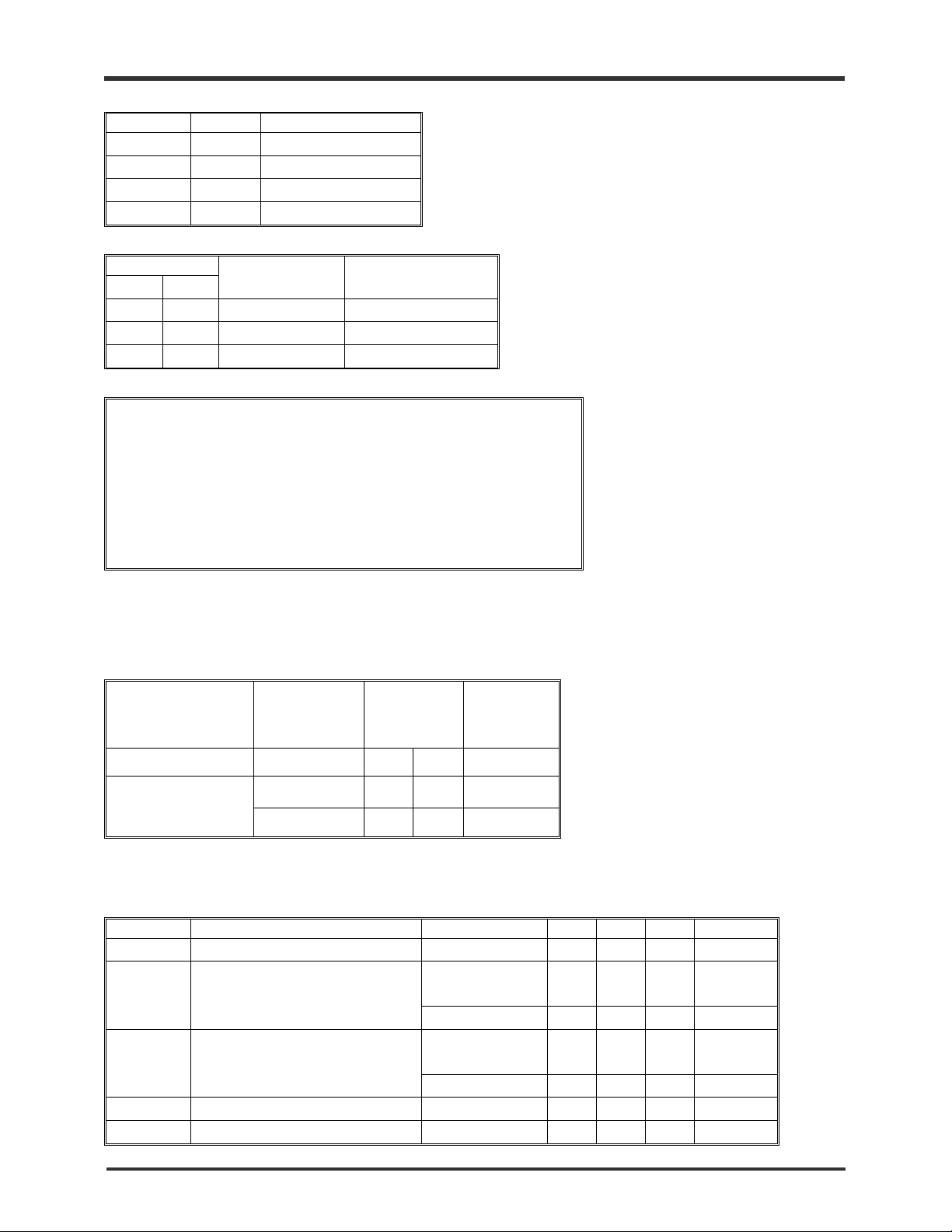
Figure 1. Functional Block Diagram Figure 2. Pin Configuration
S
QSOP
/E
16
15
14
13
12
11
10
9
Y
Y
Y
Y
C
D
S
I0
I0
I1
I0
I1
I1
I0
I1
B
B
C
C
D
D
GND
B
1
I0
2
A
I1
3
A
Y
4
A
I0
B
5
I1
B
6
Y
B
7
8
(All Pins Top View)
V
/E
I0
I1D
Y
I0C
I1
Y
CC
D
D
C
C
2000-11-28 Page 1 MDSS-0001-01
Vaishali Semic onductor 747 Camden Avenue, Suite C Cam pbel l CA 95008 P h. 408.377.6060 Fax 408.377.6063
www.vaishali.com
VS3V257/VS3V2257
Table 1. Pin Description
Name I/O Description
I0X, I1X I/O Data Input or Output
S I Select Input
/E I Enable Input
YA - YD I/O Data Output or Input
Table 2. Function Table
Inputs Path Function
/E S
H X Hi Impedance Disable all switches
L L IOX <-> YX Select 0
L H I1X <-> YX Select 1
Table 3. Absolute Maximum Ratings
Supply Voltage to Ground………………………….…..-0.5V to +4.6V
DC Switch Voltage VS……………………….………….-0.5V to +4.6V
DC Input Voltage VIN…………………………………...-0.5V to +4.6V
AC Input Voltage (Pulse Width < 20ns)……………….…………-3.0V
DC Output Sink Current per Switch Pin…………………...…..128 mA
Maximum Power Dissipation…………………………….…..0.5 Watts
Storage Temperature………………………………...-65oC to +150oC
Note ABSOLUTE MAXIMUM CONTINUOUS RATINGS are those values beyond which damage to the device may occur. Exposure
to these conditions or conditi ons beyond those indicated may adversely affect device reliability. Correct functional operation
while operating in the absolute maximum rated conditions is not implied.
Table 4. Capacitance
TA = 25oC, f = 1 MHz, VIN = 0V, V
OUT
= 0V
QSOP
Pins Operation Typ Max Unit
Control Inputs 4 5 pF
VSwitch Channels Demux 5 7 pF
(Switch OFF) Mux 7 8 pF
Note Capacitance is guaranteed, but not production tested. Total capac i tance of a path, when the switch is clos ed, i s the sum of the
switch terminal capac i tances.
Table 5. Recommended Operating Conditions
Symbol Parameter Conditions Min Typ Max Units
VCC Power supply voltage 2.3 3.6 V
VIL Low level input voltage
(Control inputs)
Vcc = 2.3 to 2.7
0.7
V
Vcc =2.7 to 3.6 0.8
VIH High level input voltage
(Control inputs)
Vcc = 2.3 to 2.7
1.7 V
Vcc = 2.7 to 3.6 2.0
TA Operating free-air temperature -40 85
o
C
Note: All unused control inputs of the device must be held at Vcc or GND, to ensure proper device operation
2000-11-28 Page 2 MDSS-0001-01
www.vaishali.com
Vaishali Semic onductor 747 Camden Avenue, Suite C Cam pbel l CA 95008 P h. 408.377.6060 Fax 408.377.6063
 Loading...