

Vaishali Semiconductor VS3244QX, VS3244Q, VS32244QX, VS32244Q Datasheet
VS3244 / VS32244
A
0
/
CC
5 6
/
High Speed CMOS VSwitch
Dual 4-Bit Bus Switches
Applications
•= 5V to 3.3V translation in mixed-supply environment
•= Hot-swap interface
General Description
The VS3244 and VS32244 are high-speed TT L–compatible dual 4-bit bus switches. The VS3244 contains
two banks of 4-bit switches, with one com mon active low enable (/G) per bank. The low ON resistance of the
VS3244 allows inputs to be connected to outputs, without adding propagation delay and without generating
additional signal noise. The VS32244 has 25Ω resistors in series with the switches to r educe gr ound-bounc e
noise and signal reflection.
The VS3244 and VS32244 bus switches are function and pinout compatible with QS3244 and CBT3244
switches. They enable 5V to 3.3V translation when used with a diode in the power supply line. In addition,
the high off-isolation in the ‘disable’ mode makes VS3244 and VS32244 ideal interface elements for hot-swap
applications.
•= Logic replacement
•= Bus isolation
/1G
Features
•= Enhanced N-FET with no DC path to VCC
or GND in normal operating signal voltage
range.
•= Low impedance bidirectional data flow:
5Ω (VS3244) and 25Ω (VS32244)
•= Pin-compatible with QS3244 and CBT3244
switches.
•= Near-zero propagation delay
•= Zero added ground bounce or signal noise
•= TTL-compatible control signals
•= Undershoot clamp diodes on all switch and
control pins
•= ESD rating >2000V (Human Body Model)
or >200V (Machine Model)
•= Latch-up current >100mA
•= Available- Available in 150-mil wide QSOP
package
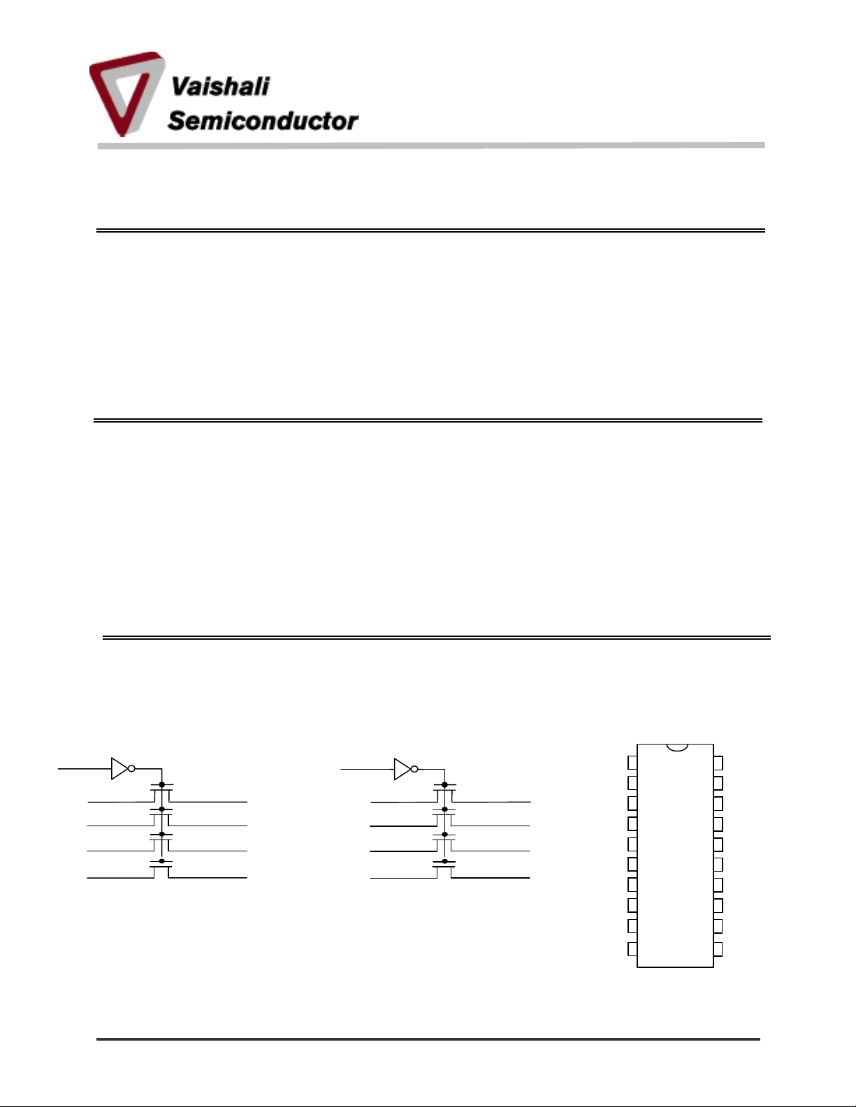
Figure 1. Functional Block Diagram Figure 2. Pin Configuration
(All Pins Top View)
/1G
1A1
2B4
1A2
2B3
1A3
2B2
1A4
2B1
GND
1
2
3
4
7
8
9
10
1A2
1A3
1A4
2G
1B1
1B4
2A2
2A3
2A4
2B1
2B4
QSOP
20
19
18
17
16
14
13
12
11
15
V
2G
1B1
2A4
1B2
2A3
1B3
2A2
1B4
2A1
2001-04-12 Page 1 MDSS-0008-02
Vaishali Semic onductor 747 Camden Avenue, Suite C Campbell CA 95008 Ph. 408.377.6060 Fax 408.377.6063
www.vishali.com

VS3244/VS32244
Table 1. Pin Description
Name I/O Description
1A1 – 1A4
2A1 – 2A4
/1G, /2G I Enable Input
1B1 – 1B4
2B1 – 2B4
I/O Data Input or Output
I/O Data Output or Input
Table 2. Function Table ( Each 4-bit bus switch)
Input Path Function
/nG
H Hi Impedance Disable all switches
L Switch Closed A port = B port
Table 3. Absolute Maximum Ratings
Supply Voltage to Ground………………………….…..-0.5V to +7.0V
DC Switch Voltage VS……………………….………….-0.5V to +7.0V
DC Input Voltage VIN………………………………… ...-0.5V to +7.0V
AC Input Voltage (Pulse Width < 20ns)……………….…………-3.0V
DC Output Sink Current per Switch Pin…………………...…..120 mA
Maximum Power Dissipation…………………………….…..0.5 Watts
Storage Temperature………………………………...-65oC to +150oC
ABSOLUTE MAXIMUM CONTINUOUS RATINGS are those values beyond which damage to the device may occur.
Exposure to these conditions or conditions beyond those indicated may adversely affect device reliability.
Correct functional operation while operating in the absolute maximum rated conditions is not implied.
Table 4. Capacitance
TA = 25oC, f = 1 MHz, VIN = 0V, V
OUT
= 0V
QSOP
Pins Typ Max Unit
Control Inputs 4 5 pF
VSwitch Channels
(Switch OFF)
Note Capacitance is guaranteed, but not production tested. Total capacitance of a path, when the switch is closed, is
the sum of the switch terminal capacitances.
5
7
pF
2001-04-12 Page 2 MDSS-0008-02
www.vaishali.com
Vaishali Semic onductor 747 Camden Avenue, Suite C Campbell CA 95008 Ph. 408.377.6060 Fax 408.377.6063
 Loading...