

Vaishali Semiconductor VS3125Q Datasheet
VS3125
Quad Bus Switch with
Individual Active Low Enables
Applications
•= 5v to 3.3V translation in mixed supply environment
•= Hot Swap interface
•= Video, audio switching
General Description
The VS3125 contains a set of f our high-speed, low-resist ance bus switches. Each bus switch is individually
controlled by TTL-compatible, active-low control input (/xOE). The low ON resistance of VS3125 allows
inputs to be connected to outputs without adding propagation delay and without generating additional signal
noise.
The VS3125 is function and pinout com patible with QS3125. It enables 5V to 3.3V level translation when
used with an external diode in the power supply line. In addition, the high off-isolation between switch
terminals in the ‘disable’ m ode, and the near-zero propagation delay in the ‘on’ state make the VS3V125 an
ideal interface element for hot-swapping applications.
•= Clock gating
•= Logic replacement
Features
•= Enhanced N-FET with no dc path to VCC or
GND in normal operating signal voltage range.
•= Low impedance bidirectional data flow
•= Pin-compatible with QS3125 & PI5C3125
switches
•= Zero added ground bounce or signal noise
•= TTL-compatible control signals
•= Near-zero propagation delay
•= Undershoot clamp diodes on all
switch and control pins
•= ESD rating >2000V (Human Body
Model) or >200V (Machine Model)
•= Latch-up current >100mA
•= Available in 150-mil wide QSOP
package
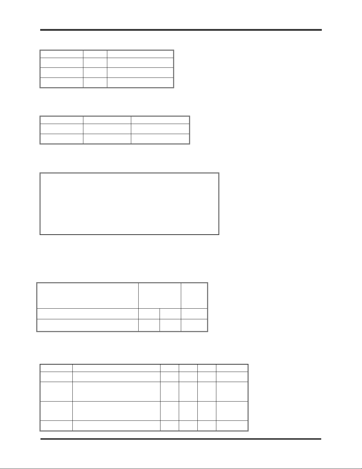
Figure 1. Functional Block Diagram Figure 2. Pin Configuration
/1OE
/2OE
/3OE
/4OE
1A 2A 3A 4A
QSOP
NC
1
/1OE
2
1A
3
1Y
4
/2OE
5
2A
6
2Y
7
GND
8
All Pins, Top View
NC= No Connect
16
15
14
13
12
11
10
V
CC
/4OE
4A
4Y
/3OE
3A
3Y
9
NC
1Y 2Y 3Y 4Y
2001-04-12 Page 1 MDSS-0011-01
Vaishali Semic onductor 747 Camden Avenue, Suite C Cam pbel l CA 95008 P h. 408.377.6060 Fax 408.377.6063
www.vaishali.com
VS3125
Table 1. Pin Description
Name I/O Description
1A – 4A I/O Data Input or Output
1Y – 4Y I/O Data Input or Output
/1OE - /4OE I Bus Switch Enable
Table 2. Function Table
/xOE Path Function
L xA <-> xY Enable switch
H High Impedance Disable switch
Table 3. Absolute Maximum Ratings
Supply Voltage to Ground………………………….…..-0.5V to +7.0V
DC Switch Voltage VS……………………….………….-0.5V to +7.0V
DC Input Voltage VIN…………………………… ……...-0.5V to +7.0V
AC Input Voltage (Pulse Width < 20ns)……………….…………-3.0V
DC Output Sink Current per Switch Pin…………………...…..120mA
Maximum Power Dissipation…………………………….…..0.5 Watts
Storage Temperature………………………………...-65oC to +150oC
Note ABSOLUTE MAXIMUM CONTINUOUS RATINGS are those values beyond which damage to the device may
occur. Exposure to these conditions or conditions beyond those indicated may adversely affect device reliability.
Functional operation under absolute maximum rated conditions is not implied.
Table 4. Capacitance
TA = 25oC, f = 1MHz, VIN = 0V, V
OUT
= 0V
QSOP
Pins Typ Max Unit
Control Inputs 4 5 pF
VSwitch Channels ( Switch OFF ) 5 7 pF
Note Capacitance is guaranteed, but not production tested. Total capacitance of a path, when the switch is closed, is
the sum of the switch terminal capacitances.
Table 5. Recommended Operating Conditions
Symbol Parameter Min Typ Max Units
VCC Power supply voltage 4.5 5.5 V
VIL Low level input voltage
(Control inputs)
VIH High level input voltage
(Control inputs)
TA Operating free-air temperature -40 85
Note: All unused control i nputs of the device must be held at Vcc or GND, to ensure proper device operation
2001-04-12 Page 2 MDSS-0011-01
Vaishali Semic onductor 747 Camden Avenue, Suite C Cam pbel l CA 95008 P h. 408.377.6060 Fax 408.377.6063
-0.5 0.8 V
2.0 5.5 V
o
C
www.vaishali.com
 Loading...