

Vaishali Semiconductor VN16118L2, VN16118L1 Datasheet
Applications
Preliminary
VN16118
SERDES Gigabit Ethernet Transceiver
• Gigabit Ethernet Up-links
• High Speed Proprietary
interface
• Backplane Serialization
• Bus Extender
General Description
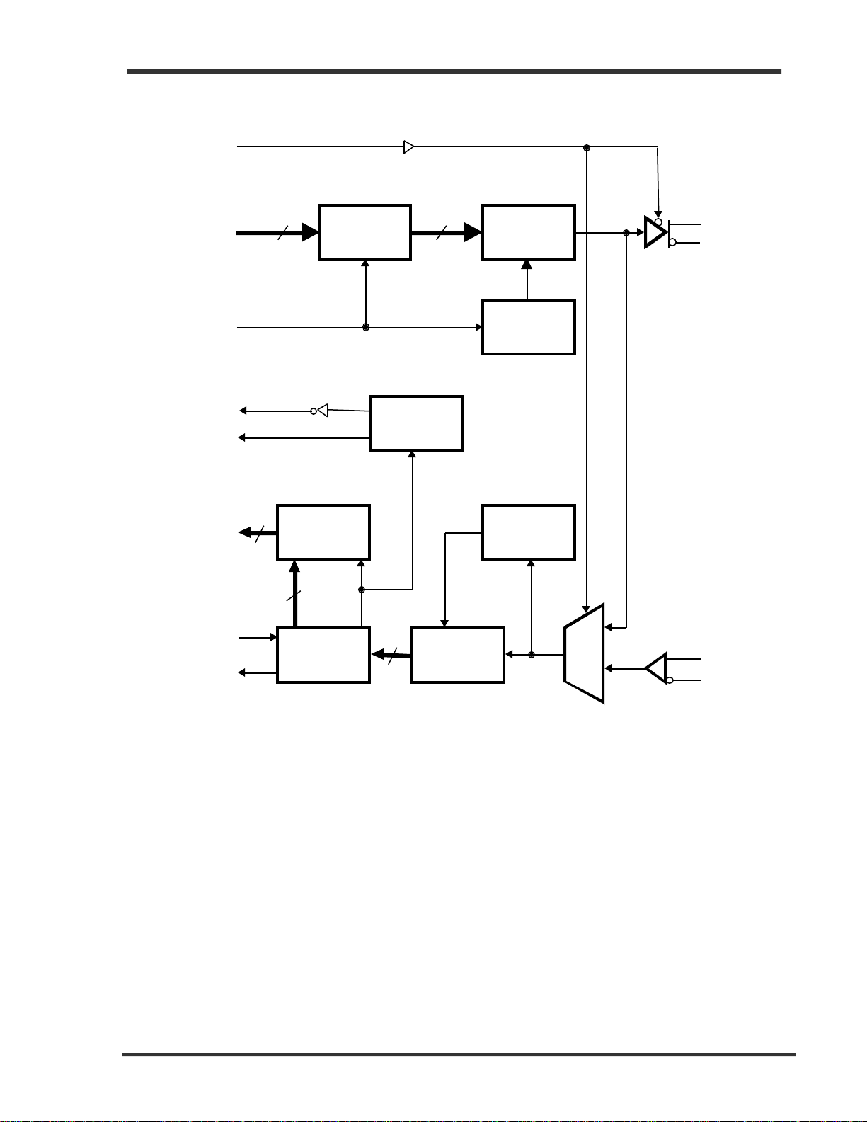
The VN16118 is a single chip,1.25 Gigabits per second Ethernet transceiver. It performs all the
functions of the Physical Medium Attachment (PMA) portion of the Physical layer, as specified
by the IEEE 802.3z Gigabit Ethernet standard. These functions include parallel-to-serial and
serial-to-parallel conversion, clock generation, clock data recovery, and word synchronization.
In addition, an internal loopback function is provided for system debugging.
The VN16118 is ideal for Gigabit Ethernet, serial backplane and proprietary point-to-point
applications. The device supports both 1000BASE-LX and 1000BASE-SX fiber-optic media,
and 1000BASE-CX copper media.
The transmitter section of the VN16118 accepts 10-bit wide parallel TTL data and converts it to
a high speed serial data stream. The parallel data is encoded in 8b/10b format. This
incoming parallel data is latched into an input register, and synchronized on the rising edge of
the 125 MHz reference clock supplied by the user. A phase locked loop (PLL) locks to the 125
MHz clock. The clock is then multiplied by 10 to produce a 1.25 GHz serial clock that is used
to provide the high speed serial data output. The output is sent through a Pseudo Emitter
Coupled Logic (PECL) driver. This output connects directly to a copper cable in the case of
1000BASE-CX medium, or to a fiber optic module in the case of 1000BASE-LX or 1000BASE
SX fiber optic medium.
The receiver section of the VN16118 accepts a serial PECL-compatible data stream at a 1.25
Gbps rate, recovers the original 10-bit wide parallel data format, and retimes the data. A Phase
Lock Loop (PLL) locks on to the incoming serial data stream, and recovers the 1.25 GHz high
speed serial clock and data. This is accomplished by continually frequency locking on to the
125 MHz reference clock, and by phase locking on to the incoming data stream. The serial
data is converted back to parallel data format. The ‘comma’ character is used to establish byte
alignment. Two 62.5 MHz clocks, 180 degrees out of phase, are recovered. These clocks are
alternately used to clock out the parallel data on the rising edge. This parallel data is sent to
the user in TTL-compatible form.
Features
• IEEE 802.3z Gigabit Ethernet
Compliant
• Supports 1.25 Gbps Using NRZ Coding
over uncompensated twin-coax cable
• Fully integrated CMOS IC
• Low Power Consumption
• ESD rating >2000V (Human Body
Model) or >200V (Machine Model)
• 5-Volt Input Tolerance
• Fully Compatible with HP HDMP-
1636/HDMP-1646 and Vitesse
VCS7135 transceivers
• Available in both 10 mm x 10 mm
and 14 mm x 14 mm LQFP
Packages
1999-12-15 Page 1 MDSN-0001-00
Vaishali Semiconductor l 747 Camden Avenue l Campbell l CA 95008 l Ph. 408.379.2900 l Fax 408.379.2937
VN16118 Preliminary
Figure 1. Functional Block Diagram
EWRAP
TX<9:0>
TX_CLK
RX_CLK<1>
RX_CLK<0>
RX<9:0>
10
10
Output Latch
10
Input Data Latch
62.5 MHz
62.5 MHz
÷ 2
125 MHz
10
Shift Registers
TX PLL Clock
Generator
RX PLL Clock
Recovery
DOUT+
DOUT-
EN_CDET
COM_DET
FRAME
ENABLE
10
Shift
Registers
INPUT
SELECTOR
DIN+
DIN-
1999-12-15 Page 2 MDSN-0001-00
Vaishali Semiconductor l 747 Camden Avenue l Campbell l CA 95008 l Ph. 408.379.2900 l Fax 408.379.2937
VN16118 Preliminary
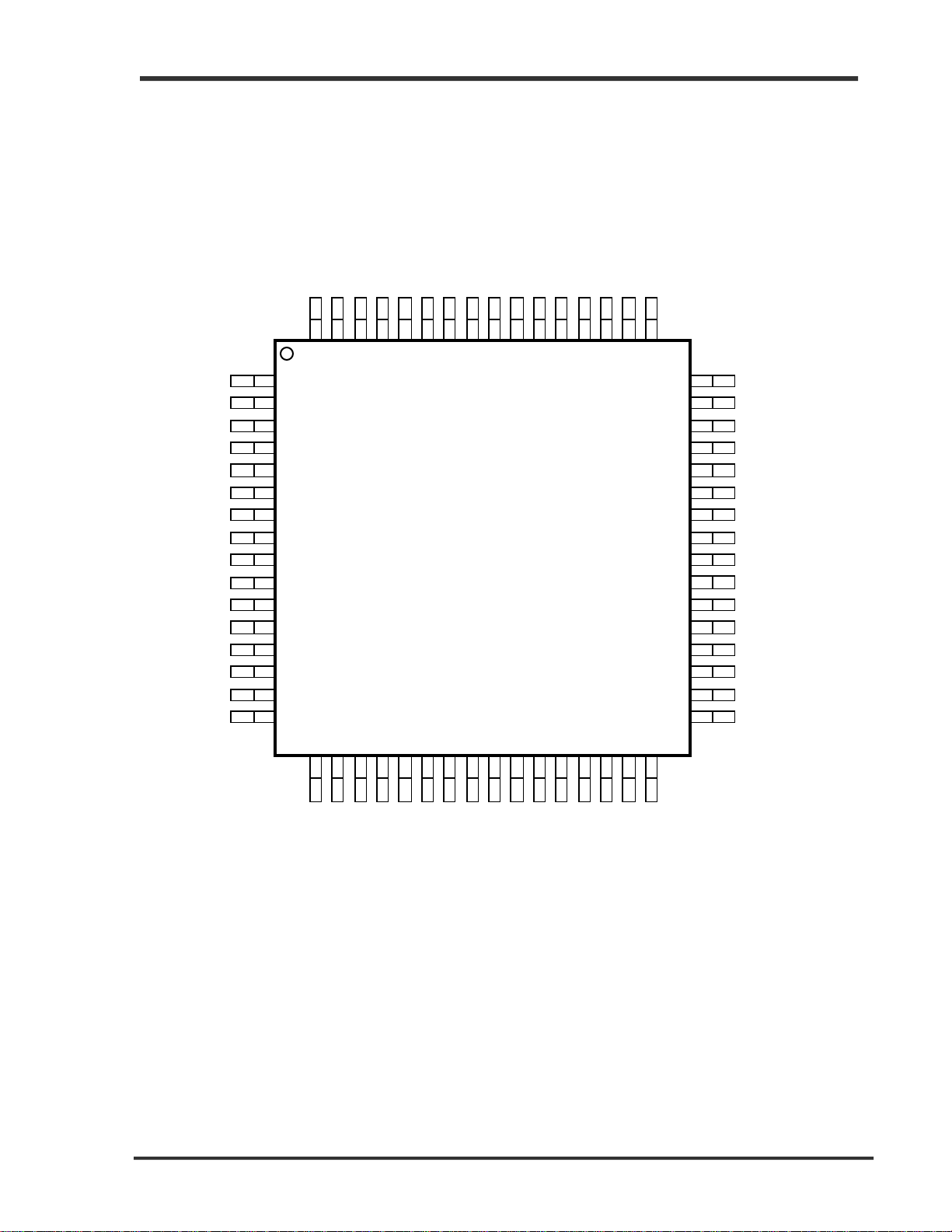
Figure 2. Pin Configuration (Top View)
GND_TX_HS
VCC_TX_HS
DOUT+61DOUT-60VCC_TX_ECL
64
63
62
1GND_ESD
2TX<0>
3TX<1>
4TX<2>
5VCC_ESD
6TX<3>
7TX<4>
8TX<5>
9TX<6>
10VCC_ESD
11TX<7>
12TX<8>
13TX<9>
14GND_ESD
15GND_TXA
16NC
17NC18
19
20
21
VCC_RXA
GND_RXA
59
58
22
23
VCC_RXA
GND_RX_ESD
57
56
24
25
VCC_RX_ESD
DIN+53VCC_RX_ESD
55
54
26
27NC28
DIN-51GND_RXF
VCC_RXF
52
50
29
30
31
NC
49
48 NC
47 COM_DET
46 GND_RXT
45 RX<0>
44 RX<1>
43 RX<2>
42 VCC_RXT
41 RX<3>
40 RX<4>
39 RX<5>
38 RX<6>
37 VCC_RXT
36 RX<7>
35 RX<8>
34 RX<9>
33 GND_RXT
32
EWRAP
VCC_TXA
1999-12-15 Page 3 MDSN-0001-00
Vaishali Semiconductor l 747 Camden Avenue l Campbell l CA 95008 l Ph. 408.379.2900 l Fax 408.379.2937
TX_CLK
VCC_TXD
GND_TXD
EN_CDET
VCC_RXD
GND_RXD
SIG_DET
VCC_RX
VCC_RXD
RX_CLK<1>
GND_RX
RX_CLK<0>
 Loading...