

Page 1
3
8
9
A
A1A2A3A4A
A6A
/
查询VS32245Q供应商
VS3245 / VS32245
High Speed CMOS VSwitch
8-Bit Bus Switches
Applications
•= 5V to 3.3V translation in mixed-supply environment
•= Hot-swap interface
General Description
The VS3245 and VS32245 are high-speed T TL–compatible 8-bit bus switches. The VS3245 contains eight
high-speed bus switches, with a comm on active low enable (/OE). The low ON resistance of the VS3245
allows inputs to be connected to outputs, without adding propagation delay and without generating additional
signal noise. The VS32245 has 25Ω resistor s in s er ies with the switches to r educ e ground- bounce noise and
signal reflection.
The VS3245 and VS32245 bus switches are function and pinout compatible with QS3245 and CBT3245
switches. They enable 5V to 3.3V translation when used with a diode in the power supply line. In addition,
the high off-isolation in the ‘disable’ mode makes VS3245 and VS32245 ideal interface elements for hot-swap
applications.
•= Logic replacement
•= Bus isolation
Features
•= Enhanced N-FET with no DC path to VCC
or GND in normal operating signal voltage
range.
•= Low impedance bidirectional data flow:
5Ω (VS3245) and 25Ω (VS32245)
•= Pin-compatible with QS3245 and CBT3245
switches.
•= Near-zero propagation delay
•= Zero added ground bounce or signal noise
•= TTL-compatible control signals
•= Undershoot clamp diodes on all switch and
control pins
•= ESD rating >2000V (Human Body Model)
or >200V (Machine Model)
•= Latch-up current >100mA
•= Available in 150-mil wide QSOP package
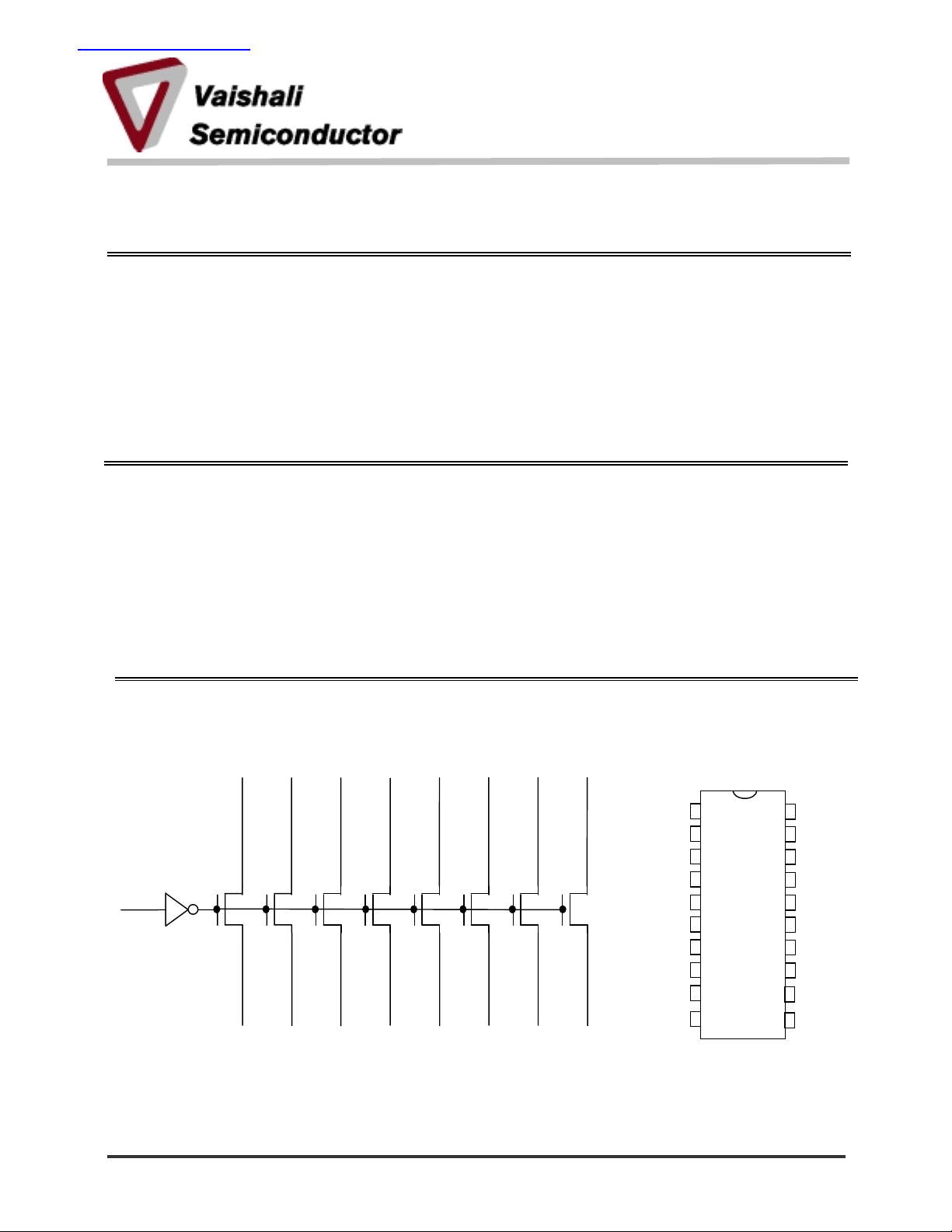
Figure 1. Functional Block Diagram Figure 2. Pin Configuration
A0
A1 A2 A3 A4 A5 A6 A7
(All Pins Top View)
QSOP
/OE
B2
B3 B4 B5 B6
B7B0 B1
GND
NC
0
5
7
1
2
4
5
6
7
10
20
19
18
17
16
14
13
12
11
15
V
OE
B0
B1
B2
B3
B4
B5
B6
B7
2001-04-12 Page 1 MDSS-0007-02
Vaishali Semic onductor 747 Camden Avenue, Suite C Cam pbel l CA 95008 P h. 408.377.6060 Fax 408.377.6063
www.vaishali.com
Page 2
VS3245/VS32245
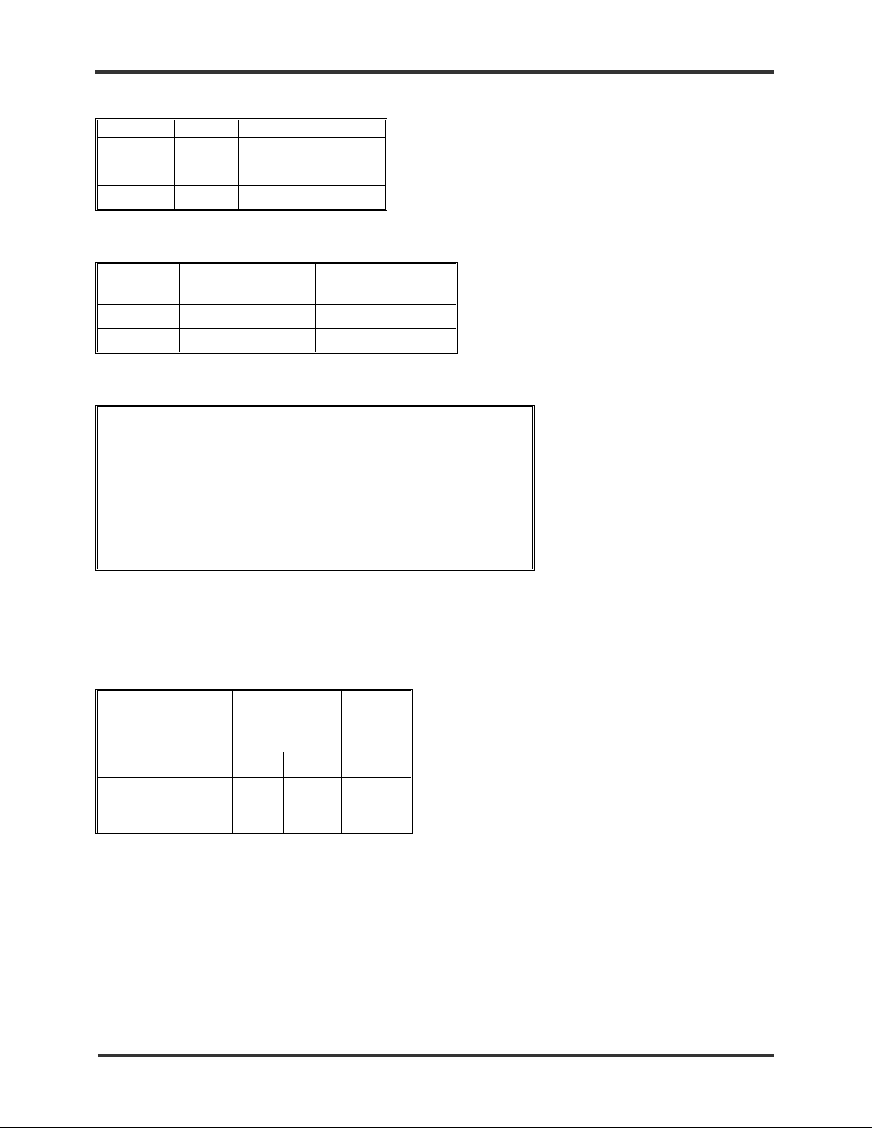
Table 1. Pin Description
Name I/O Description
A0 - A7 I/O Data Input or Output
/OE I Enable Input
B0 – B7 I/O Data Output or Input
Table 2. Function Table
Input Path Function
/OE
H Hi Impedance Disable all switches
L An <-> Bn A
= Bn
n
Table 3. Absolute Maximum Ratings
Supply Voltage to Ground………………………….…..-0.5V to +7.0V
DC Switch Voltage VS……………………….………….-0.5V to +7.0V
DC Input Voltage VIN………………………………… ...-0.5V to +7.0V
AC Input Voltage (Pulse Width < 20ns)……………….…………-3.0V
DC Output Sink Current per Switch Pin…………………...…..120 mA
Maximum Power Dissipation…………………………….…..0.5 Watts
Storage Temperature………………………………...-65oC to +150oC
Note ABSOLUTE MAXIMUM CONTINUOUS RATINGS are those values beyond which damage to the device may
occur. Exposure to these conditions or conditions beyond those indicated may adversely affect device reliability.
Correct functional operation while operating in the absolute maximum rated conditions is not implied.
Table 4. Capacitance
TA = 25oC, f = 1 MHz, VIN = 0V, V
OUT
= 0V
QSOP
Pins Typ Max Unit
Control Inputs 4 5 pF
VSwitch Channels
(Switch OFF)
Note Capacitance is guaranteed, but not production tested. Total capacitance of a path, when the switch is closed, is
the sum of the switch terminal capacitances.
5
7
pF
2001-04-12 Page 2 MDSS-0007-02
www.vaishali.com
Vaishali Semic onductor 747 Camden Avenue, Suite C Cam pbel l CA 95008 P h. 408.377.6060 Fax 408.377.6063
Page 3
VS3245/VS32245
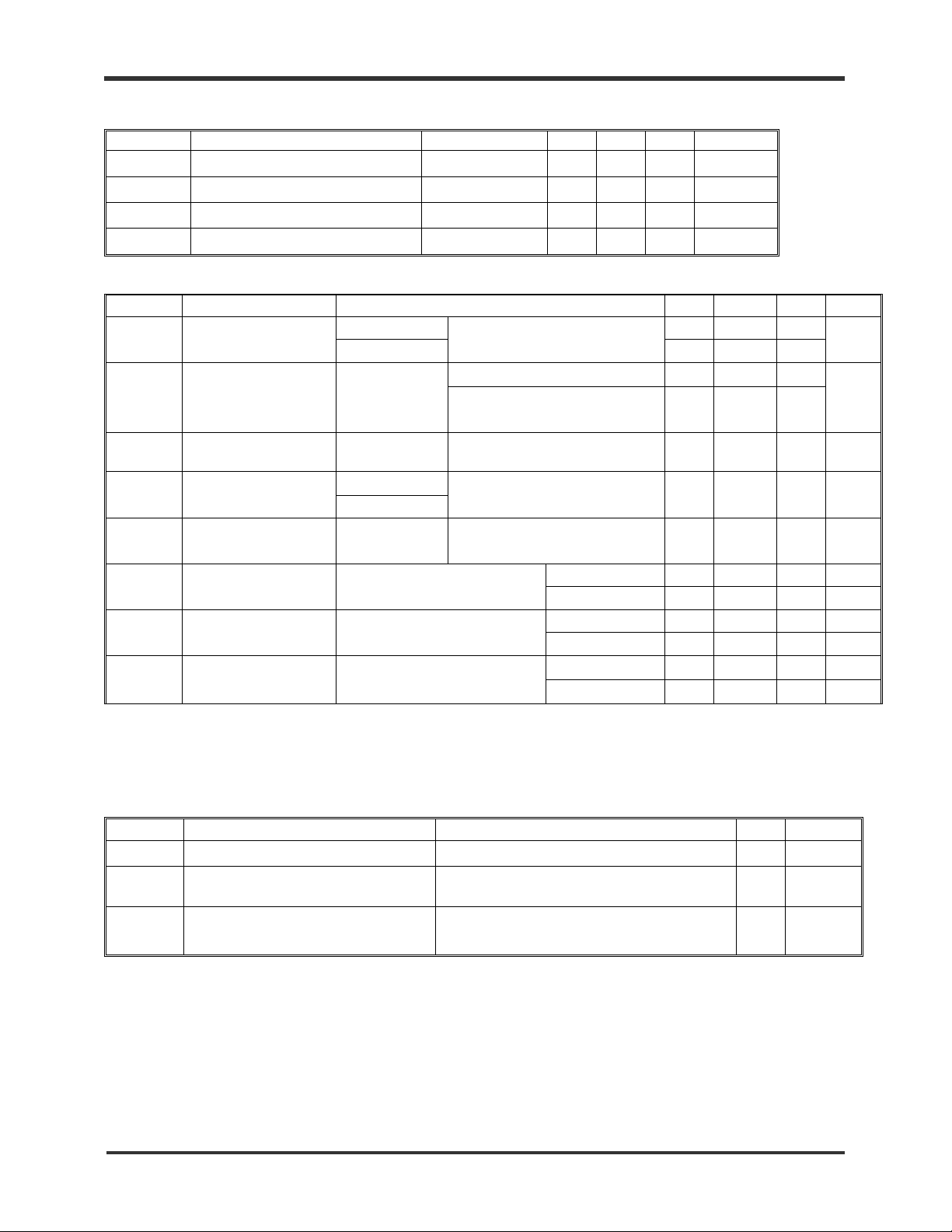
Table 5. Recommended Operating Conditions
Symbol Parameter Conditions Min Typ Max Units
VCC Power supply voltage 4.5 5.5 V
VIL Low level input voltage -0.5 0.8 V
VIH High level input voltage 2.0 5.5 V
TA Operating free-air temperature -40 85
o
C
Table 6. Electrical Characteristics Over Recommended Operating Free-air Temperature Range
Symbol Parameter Test Conditions Min Typ
Control Input -1.5 VIK Clamp Voltage
Switch I/O
VOH Logic High Voltage Switch I/O
I
I
Input Leakage
Control Input VCC = Max, VI = VCC or GND 1
Current
| Power OFF Leakage
OFF
Current
|IOZ| OFF State Leakage
Control Input |
Switch I/O
Switch I/O VCC = Max, V
Current
Switch I/O Drive
ODL
Current (Logic LOW)
Switch I/O Drive
ODH
Current (Logic HIGH)
RON Switch ON
Resistance
(2)
VCC = Min, VIN = 0,
= 0.4V
V
OUT
VCC = Min, VIN = VCC,
= 2.4V
V
OUT
= Min, VIN = 0,
V
CC
= 30mA
I
OUT
VCC = Min, IIK = -18 mA
VIN = VCC = 5V, I
OUT
= -5µA
VCC = 4.3V, VN = 5V,
= -5µA
I
OUT
V
= 0,
CC
or VO = VCC or GND
V
I
= VCC,
I/O
/OE = V
CC
VS3245 50 mA I
VS32245 mA
VS3245 -50 mA I
VS32245 mA
VS3245 5 7
VS32245 20 28 40
-1.5
3.7 3.9 4.1
3.0 3.3 3.6
1
1
(1)
Max Units
Notes:
1. Typical values are specifi ed at V
2. R
is measured by forcing specified current into the ‘output ’ node of the switch with the ‘input’ node of the switch at the the
ON
specified voltage
= 5.0V and TA = 25oC.
CC
V
V
µA
µA
µA
Ω
Ω
Table 7. Power Supply Characteristics Over Recommended Operating Free-air Temperature Range
Symbol Parameter Test Conditions
I
Quiescent Power Supply Current VCC = Max, /OE = VCC or GND, f = 0 1
CCQ
∆ICC
Q
Dynamic Power Supply Current
CCD
Power Supply Current per Input High
(Control Input)
(2)
= Max, VIN = 3.4V, f = 0 1.5 mA
V
CC
(3)
VCC = Max, Switch pins open,
Control Inputs toggling at 50% duty cycle
(1)
Max Units
µA
0.25 mA/MHz
Notes:
1. For conditions shown as Min or Max, use the appropriate values per Recommended Operating Conditions.
2. Per TTL-driven control input. All other control inputs at GND. Switch I /O pins do not contribute to ∆ICC.
3. This parameter represents the average DC current resulting from the switching of internal nodes of the device at a given
frequency. The switch I/O pins make insignificant contribution to the dynamic power supply c urrent of the device. This paramete r
is guaranteed, but not producti on t ested.
2001-04-12 Page 3 MDSS-0007-02
www.vaishali.com
Vaishali Semic onductor 747 Camden Avenue, Suite C Cam pbel l CA 95008 P h. 408.377.6060 Fax 408.377.6063
Page 4
VS3245/VS32245
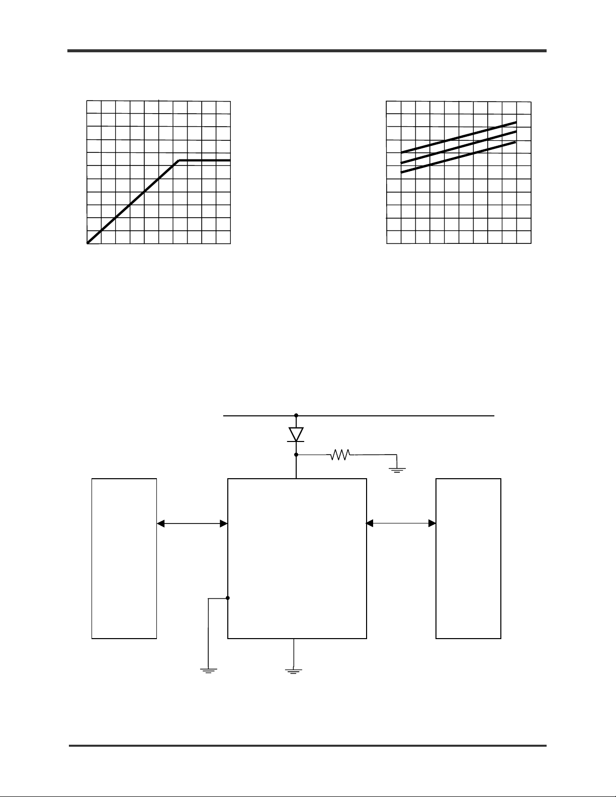
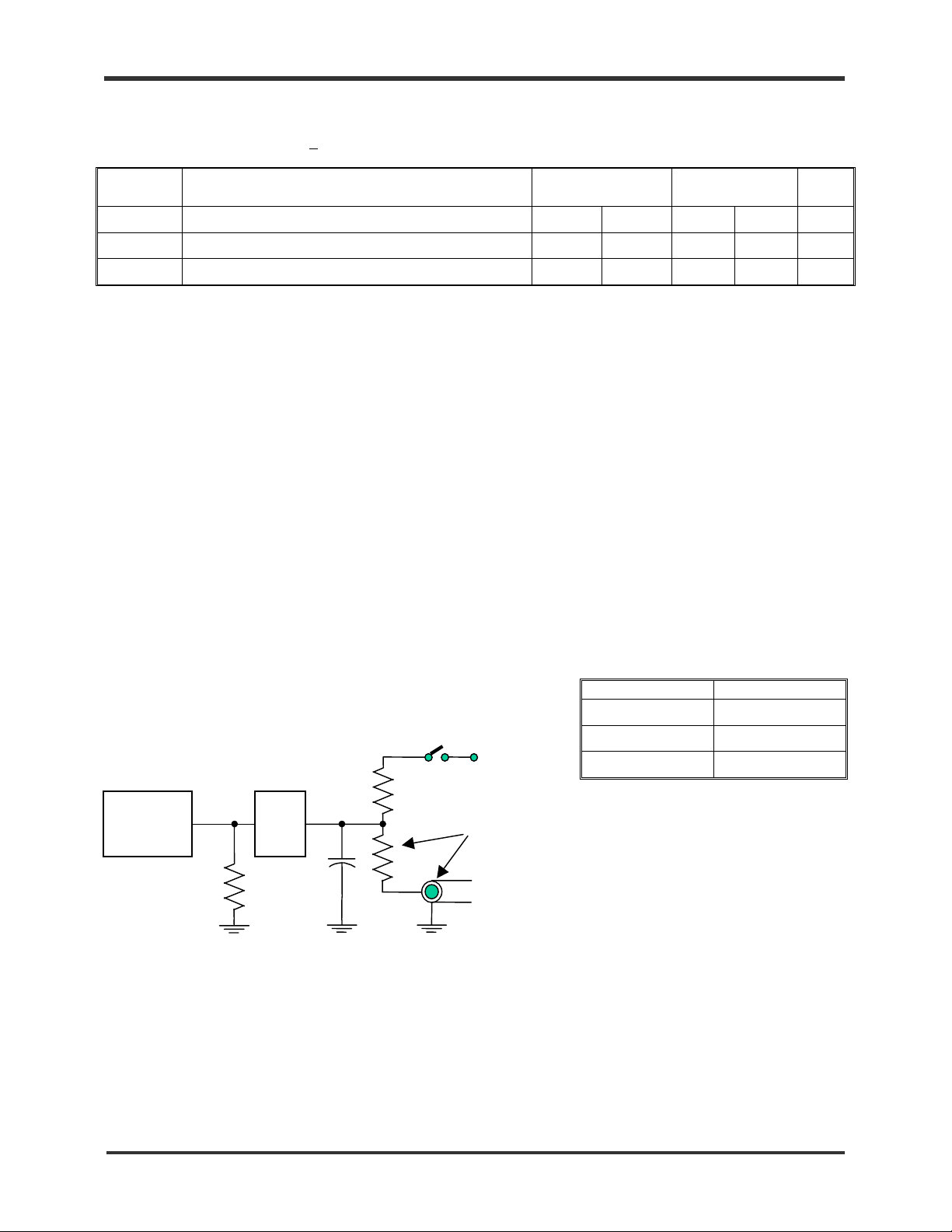
Figure 3. VOLTAGE TRANSLATION
Figure 4. VOH CHARACTERISTICS
5
4.5
Vout
(V)
4
3
2
VCC = 4.3V
VOH
Output Voltage
(V)
4.0
3.5
3.0
2.5
0
0
Vin (V)
5
2.0
4.75
4.5
VCC – Supply Voltage (V)
Figure 5. Voltage Translation Application
VCC = 5V
1N4148
or equivalent
10K
VCC
5V
DEVICE
I/O
VS3245
VS32245
I/O
3.3V
DEVICE
/OE
TA = 85°C
TA = 25°C
TA = - 40°C
5.5
2001-04-12 Page 4 MDSS-0007-02
www.vaishali.com
Vaishali Semic onductor 747 Camden Avenue, Suite C Cam pbel l CA 95008 P h. 408.377.6060 Fax 408.377.6063
Page 5
VS3245/VS32245
Table 8. Switching Characteristics Over Operating Range
TA = -40oC to +85oC, VCC = 5.0V + 10%
C
= 50pF, R
LOAD
Symbol
t
, t
Data Propagation Delay
PHL
, t
Switch Turn-on Delay, /OE to An, Bn 0.5 5.6 0.5 6.6 ns
PZL
, t
Switch Turn-off Delay /OE to An, B
PHZ
t
t
PLH
PZH
PLZ
Notes:
1. See test circuit s and waveforms.
2. This parameter is the c al culated theoretical RC time constant of ON-state resistance of the switch and the specif i ed l oad
capacitance when driven by an ideal voltage sourc e (zero source impedance). This time-constant is on the order of 0. 25 ns for
VS3245 and 1.25 ns for VS32245. S i nce this time-constant is much smaller t han ri se/fall times of t ypical driving signals, it adds
very little propagation delay to the system.
3. This parameter is guaranteed, but not production tested.
= 500Ω unless otherwise stated.
LOAD
Description
(2,3)
through the switch 0.25 1.25 ns
(1)
0.5 4.5 0.5 4.5 ns
n
VS3245
(3)
Min
Max
VS32245
(3)
Min
Max Units
Figure 6. AC Test Circuit and Switching Waveforms
AC Test Circuit Load Switch
Pulse
Generator
50
Ω
V
IN
DUT
C
V
L
OUT
500
450
S
1
7 V
Ω
R
L
Ω
50Ω=Coax to
Oscilloscope
t
PLH
t
PLZ
t
PHZ
Input Conditions
Input voltage = 0 V to 3.0 V
t
= tf = 2.5ns (10% to 90%)
r
Position
TEST S1
, t
Open
PHL
, t
Closed
PZL
, t
Open
PZH
2001-04-12 Page 5 MDSS-0007-02
www.vaishali.com
Vaishali Semic onductor 747 Camden Avenue, Suite C Cam pbel l CA 95008 P h. 408.377.6060 Fax 408.377.6063
Page 6
VS3245/VS32245
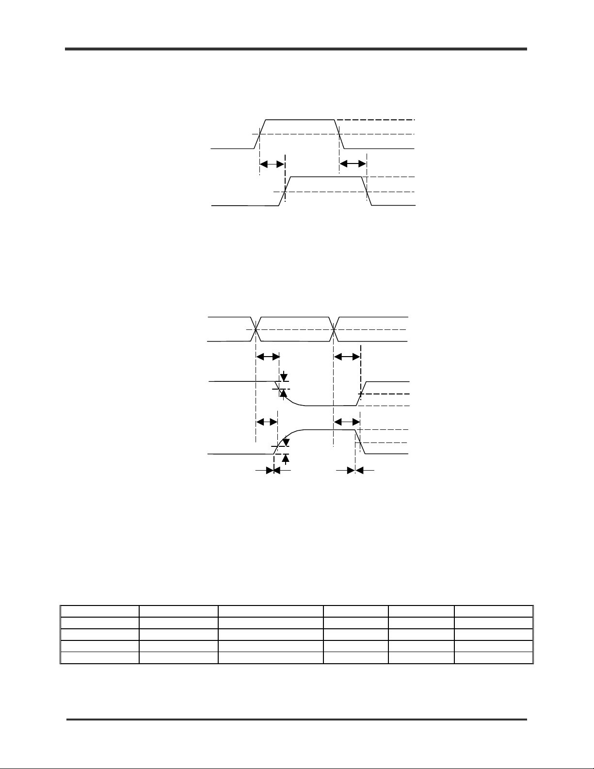
Switching Waveforms
3.0 V
Input
Switch Output
Control Input
tPLH tPHL
Propagation Delay
tPHZ
tPZH
1.5 V
0 V
V
1.5 V
V
3.0 V
1.5 V
0 V
OH
OL
VOH
1.5 V
0 V
3.5 V
1.5 V
V
OL
Switch Output
(Switch Input = 3.0 V)
Switch Output
(Switch Input = 0 V)
0.3 V
tPLZ
0.3 V
Switch ON Switch OFF
tPZL
Switch ON
Enable and Disable Times
Ordering Information
Part Number Marking Shipping/Packaging No. of Pins Package Temperature
VS3245Q VS3245Q Tubes 20 QSOP
VS3245QX VS3245Q Tape & Reel 20 QSOP
VS32245Q VS32245Q Tubes 20 QSOP
VS32245QX VS32245Q Tape & Reel 20 QSOP
-40°C to +85°C
-40°C to +85°C
-40°C to +85°C
-40°C to +85°C
2001-04-12 Page 6 MDSS-0007-02
www.vaishali.com
Vaishali Semic onductor 747 Camden Avenue, Suite C Cam pbel l CA 95008 P h. 408.377.6060 Fax 408.377.6063
 Loading...