

V3 Semiconductor V96SSC-33LP Datasheet
Copyright © 1997, V3 Semiconductor Corp. V96SSC Data Sheet Rev 2.3
1
V96SSC
Rev. B1
HIGH-INTEGRA TIO N SYSTEM CONTROLLER
FOR i960Sx/Jx AND PowerPC™ 401Gx
PROCESSORS
V3 Semiconductor reserves the right to change the specificati ons of this product wit hout notice.
V96SSC and V96xPBC are trademarks of V3 Semiconductor. All other trademarks are the propert
y
of their respective owners.
• Direct interface to i960Sx/Jx and PPC401Gx
processors
• High-performance burst DRAM controller
• Two-channel fly-by DMA controller
• Serial communications unit
• Programmable chip-select/strobe generation
• Support for 8/16-bit boot PROMs
• Two 32-bit general purpose timers
• Pulse width modulat ion capabilit
y
• System watchdog and heartbeat timers
• 16 general purpose I/O bits
• Eight input port s and eight output ports
• Interrupt control unit
• Local bus speeds up to 33MHz
• Low cost 100-pin EIAJ PQFP package
• Fastest time to market for i960Sx and i960Jx
based designs
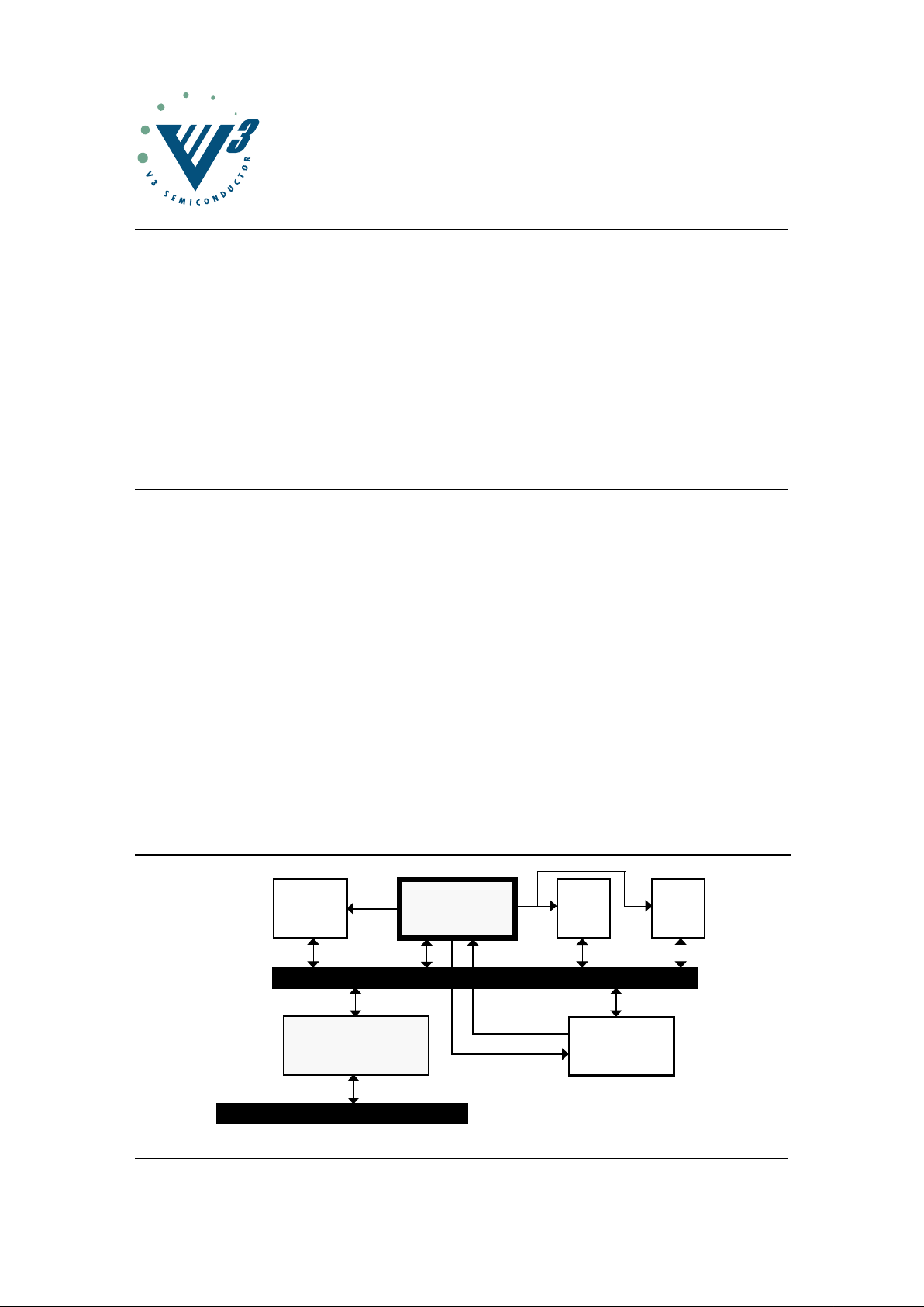
The V96SSC High-Integration System Contro ller
is a single-chip device that simplifies the design
of systems based on i960Sx, i960Jx or
PPC401Gx embedded microprocessors. The
V96SSC replac es many lower integration
components with a single, high-integration
device.
Nearly all i960 or PowerPC processor based
systems will require DRAM for code and data
storage. The V96SSC includes a highperformance DRAM controller which is
programmable to accommodate a wide range of
DRAM speeds and architectures.
The eight chip-select/strobes further simplif
y
peripheral/memo ry connection. Each se lect has
programmable timing and a total of four waitstate generators are provided.
Beyond simplifying memory and peripheral
control, the V96SSC also includes many of the
peripherals needed to build a high-performance
i960 or PPC401Gx based system: DMA
channels, synchronous/ asynchronous seri al port ,
g
eneral purpose and system heartbeat timers, bit
I/O ports, and an interrupt controller.
In addition, the V96SSC includes special
features to enhance system integrity. The bus
watch timer prevents system hangs on access to
unpopulated memory. A watchdog timer is also
included to recover from software upsets.
Due to its small footprint, and glueless interface,
the V96SSC provides the best features of an
integrated processor without any performance
compromises!
LOCAL BUS
LOCAL BUS
IRQs
DRAM
ARRAY
PROM
ADDR
CHIP SELECTS
AND STROBES
DMA REQUEST
LOCAL BUS
LOCAL BUS
PCI BUS
SYSTEM
CONTROLLER
V96SSC
DEVICE
NETWORKING
V960PBC or V961PBC
CONTROLLER
PCI BRIDGE
PPC401Gx
i960Sx/Jx
CPU
V96SSC
2
V96SSC Data Sheet Rev 2.3 Copyright © 1997, V3 Semiconductor Inc.
This document contains the product codes, pinouts, package mechanical information, DC
characteristics, and AC characteristics for the V96SSC. Detailed functional information is contained in
the User’s Manual.
V3 Semiconductor retains the rights to change documentation, specifications, or device functionality at
any time without notice. Please verify that you have the latest copy of all documents before finalizing a
design.
1.0 Product Codes
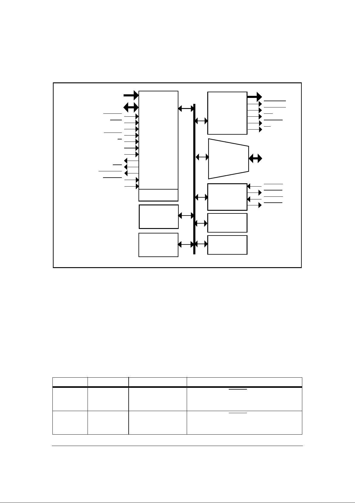
2.0 Functional Description
The V96SSC consists of the foll o wing functional units :
• Direct i960 and PPC401Gx Processors Bus Interface Unit
• Burst DRAM Controller
• DMA Controller
• Serial Communications Unit
• Chip Select/Strobe Unit
• General Purpose Timer/Counters
• System Watchdog and System Heartbeat Timers
• Interrupt Control Un it
• I/O Control Unit and Internal Signal Multiplexer
A block diagram of the V96SSC is shown in Figure 1. Each of the functional units is described briefly in
the sections below. The V96SSC Data Sheet provides information regarding AC and DC
specifications, pinout, and packaging. Detailed information regarding hardware and softwar e
interfacing can be found in the V96SSC User’s Manual
.
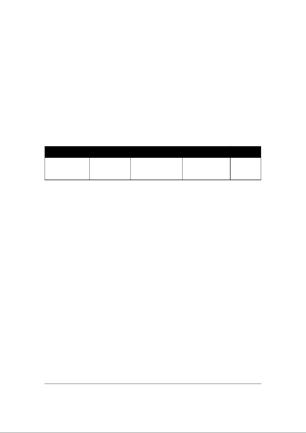
Table 1: Product Codes
Product Code Processor Bus Type Package Frequency
V96SSC-33LP
i960SA/SB
i960JA/JD/JF
PPC401GF
16-bit multiplexed
32-bit multiplexed
32-bit multiplexed
100-pin EIAJ PQFP 33MHz
V96SSC
Copyright © 1997, V3 Semiconductor Inc. V96SSC Data Sheet Rev 2.3
3
Figure 1: V96SSC Block Diagram
2.1 Direct i960 Sx/Jx and PPC401Gx Processors Bus Interface Units
The V96SSC is desi gned t o co nnect di rect ly to i96 0Sx/J x and PP C401 Gx p roces so rs. No “gl ue l ogic”
is required. Care was taken during the design of the V96SSC to insure full AC timing compatibility with
these processors running with bus speeds up to 33MHz. Even the pinout of the V96SSC has been
designed with ease of connection in mind.
At the beginning of each processor bus cycle the V96SSC samples the BTYPE[1:0] pins. As it’s shown
in the following table, these pins indicate what type of bus cycle is being run. Because the bus type is
dynamically detected, the V96SSC may be used in systems using bot h 16-bit and 32-bit masters.
Table 2: BTYPE[1:0] Pin Decoding
BTYPE[1:0] CPU Mode Boot Address Description
00 i960SA/SB A[31, 26:24]=”0000”
16-bit data bus, BE[1:0] valid for current
cycle, both processor and V96SSC use 2x
clock
01 PPC401Gx A[31, 26:24]=”1111”
32-bit data bus, BE[3:0] valid for current
cycle, processor uses 1X clock and V96SSC
uses 2X clock
A31,A[26:16]
AD[15:0]
BE[1:0]
ADS
ALE
BLAST
W/R
BTYPE[1:0]
HLDA
HOLD
INT
RESOUT
RESET
CLK2
SYSTEM
HEARTBEAT/
WATCHDOG
TIMERS
BUS WATCH
i960
PROCESSOR
INTERFACE
SERIAL
COMM
UNIT
DRAM
CONTROL
MA[11:0]
RAS[1:0]
CAS[3:0]
WE
OE[1:0]
LE
I/O[15:0]
DREQ0
DACK0
DREQ1
DACK1
DMA
TWO
CHANNEL
CHIP SELECT
STROBE
LOGIC
32-BIT
TIMERS (2)
MUX
I/O
and
BIT I/O
V96SSC
4
V96SSC Data Sheet Rev 2.3 Copyright © 1997, V3 Semiconductor Inc.
In i960Sx systems, the low order address signals are latched internal ly from the AD[15:0] bus upon
assertion of ALE. The high-orde r address lines are demul tiplexed on the i960Sx proces sor, and are
routed directly to the V96SSC’s high order address inpu ts. The i960Jx processor uses a 32-bit
multiplexed address/data bus, therefore for i960Jx bus accesses, the V96SSC latches the high order
address signals internally on the assertion of ALE.
All accesses to V96SSC’s internal registers are performed via the AD[15:0] lines. In 32-bit i960Jx
systems, the internal registers are typic ally accessed in a 32 bit r egion where ac cess to the internal
registers is done by soft wa re 1 6 bi ts a t a ti me (BTY PE= "10" ). Al terna tely, it can be ma pp ed i nto a 16
bit region using BTYPE="11". While the V96SSC is internally a 16-bit device, it is capable of
supporting 32-bit memory and peripheral devi ces.
V96SSC also supports direct interface to PPC401Gx. When BTYPE=”01” then the boot address
matches that of the PPC401Gx. In this mode a cycle can be initiated with either an ALE or ADS pulse.
Since the PPC401Gx has only an ALE output and lacks an ADS (AS) pin, ADS on the V96SSC ca n be
tied high by a pull-up resistor.
2.2 Burst DRAM Controller
The V96SSC’s DRAM controller provides the following features:
• Support for fast page mode, extended data out, and Ramtron’s enhanced DRAM architectures
• Two DRAM banks of up t o 64MByte each (128MBytes total)
• Programmable DRAM bank address base and size
• Programmabl e ro w/column mult ip l ex i ng mo de
• Programmable RASx and CASx timings
• Support for 16-bit and 32-bit DRAM arrays
• Support for extended burst cycles up to 256 bytes transactions in length
• Programmable page caching to eliminate RAS cycles for subsequent accesses to the same
DRAM page
• Programmable refresh counter
• 1-0-0-0 read and 0-0-0-0 write performance at 33MHz
The burst DRAM controller is designed to support traditional fast page mode DRAMs (FPM), the new
extended data out page mode DRAMs (EDO), and Ramtron’s ultra high-performance enhanced
DRAM (Ramtron E DRAM) devices. A wide varie ty of DRAM s peeds and orga nizations may be
10
i960Jx
(32 bit bus)
A[31, 26:24]=”1110”
32-bit data bus, BE[3:0] valid for current
cycle, processor uses 1X clock and V96SSC
uses 2X clock
11
i960Jx
(16 bit bus)
A[31, 26:24]=”1110”
32-bit data bus, BE3 and BE0 valid for current cycle, processor uses 1X clock and
V96SSC uses 2X clock
Table 2: BTYPE[1:0] Pin Decoding
BTYPE[1:0] CPU Mode Boot Address Description

V96SSC
Copyright © 1997, V3 Semiconductor Inc. V96SSC Data Sheet Rev 2.3
5
accommodated due to the V96SSC’s flexib ility.
Two DRAM banks are provided. Each bank has its ow n progra mmable addre ss base and size. The
mapping of memory address lines to row and column addresses is also programmable for each bank.
The twelve mixed address lines (MA[11:0]) are shared by both banks. Each bank may be
independently enabled and/or write protected. Both banks share a common DRAM signal timing
generator that controls all DRAM timing parameters. DRAM array width can be set to either 16-bit or
32-bits; the V96SSC controls lane steering logic in mixed width systems.
FPM, EDO, and Ramtron EDRAMs a re a natural fit for burst bus p rocessors such as i960 or
PPC401Gx family. The V96SSC takes advantage of fast page mode accesses for every burst
transaction, insuring the highest transfer rate possible. The V96SSC also supports extended burst
peripherals, such as networking controllers, up to a maximum length of 64Byte data cycles.
The DRAM controller also includes page cache management logic. This logic detects subsequent
burst accesses within the same DRAM page, and eliminates the RAS precharge time and row address
cycles for these accesses. Removing these cycles can reduce the average wait-state profile for many
applications. The “aggressiveness” of the caching algorithm is programmable, and page caching can
be completely disabled. The page size is programmable from 512 to 81 92 bytes.
2.3 DMA Controller
Two independent DMA Channels are provided in the V96SSC. The DMA Controller generates fly-by
cycles to transfer data directly from the DRAM to the selected peripheral, or vice-versa. Each cha nnel
includes a req uest i nput (D REQx), an acknowledge output (DACKx), and an end-of-process outpu t
(EOPx, accessible via the I/O Multiplexer). Each channel can also be assigned to a chip select/strobe
channel to provide the necessary strobing signals to the DMA target/source peripheral.
The DMA buffer start and stop addresses ar e program mable, as i s the direc tion of tran sfer (read or
write). Transfers may be initiated either via the DREQx pins or through software.
The DMA Controller’s programmable throttle count allows long transfers to be periodically interrupted
to allow the processor access to the bus for code fetches, etc.
2.4 Serial Communications Unit (SCU)
The V96SSC’s Serial Communications Unit offers both synchronous and asynchronous modes. In
asynchronous mod e, the Serial C ommuni cations U nit fun ctions a s an ind ustry standard , ful l duplex
UART. Transmission and reception are double buffered to help prevent data overruns. Interrupts are
generated on receiver buffer full, transmit buffer empty, buffer overrun error, and framing error.
In synchronous (SPI) mode, data is moved into, or out of, the SCU’s buffers on transitions of the serial
clock output pin (SCLK). Data word length is programmable from 1 to 16 bits. An interrupt is generated
upon completi on of a n SPI t ransfe r. SPI mode is ideal f or co nnecting to serial i nterf ace per ipher als
such as A/D converters.
The clock referenc e for the Seri al Communica tions Unit can be either the independ ent baud rate
generator or general purpose timer 1.
2.5 Chip Select/Strobe Unit
The Chip Select/Strobe Unit provides all the logic necessary to interface a wide ar ray of peripherals
and memory components to the i960Sx/Jx processor. Address decoding, wait-state generation, chipselect, and read/wr ite strobe gen eration a re handled c ompletely b y the V96SSC; no glue log ic is

V96SSC
6
V96SSC Data Sheet Rev 2.3 Copyright © 1997, V3 Semiconductor Inc.
needed. Eight output strobes/selects are available as output pins from the I/O Multiplexer.
There are eight memory decode registers, each with the following options:
• Base address and size (minimum granularity 64K)
• Region data width
• Read/Write enable
Each memory decode register has an associated Region Timing Control register. This register assigns
timings for synchronous mode strobes as well as for wait-state generation. The following timings are
programmable f or each region:
• Strobe assert from bus cycle start
• Strobe de-assert from bus cycle start
• READY delay from cycle start (wait-states)
• Back-to-Back cycle delay
Each of the 8 chip select/strobe output pins is assigned to one of four programmable memory ranges.
These strobe signals can be used as asynchronous chip-selects, or combined with the timing values
for the region to create read and write strobes. Each strobe has the following programmable options:
• Address match register assignment
• Access type: read, write, both
• Timing: asynchronous, synchronous
• Sub-decode : finer granular ity decoding
The chip select/strobe unit is also tied to the DMA Controller. Each DMA channel can be assigned to a
particular decode region and its associated timing.
2.6 General Purpose Timers (GPT)
Two identical 32-bit gene ral p urpo se t imer s a re in tegr ate d in the V9 6SSC. Thes e ti mer s may be us ed
for a number of applications including: periodic interrupt generation, event counting, and pulse width
modulation.
The timers decrement every clock cycle, from a 32-bit preload value until a terminal count of zero is
reached. A maskable interrupt is generated on terminal count. The timer may be programmed to halt
on terminal count, or to reload and restart counting.
Each timer has an external input (TIx) and external output pin (TOx). The TIx pin can be used as an
edge or level sensitive start trigger. The TOx pin has the following modes:
• Latched low
• Short and long puls e low on terminal count
• Toggle on terminal count
• Pulse width modula tion
• One shot
 Loading...