

V96BMC
y
y
y
Rev. D
HIGH PERFORMANCE BURST
DRAM CONTR O LLER
FOR i960Cx/Hx/Jx PROCESSORS
• Pin/Software compatible with earlier V96BMC.
• Direct interfaces to i960Cx/Hx/Jx processors.
• 3.3V DRAM interface support.
• Near SRAM perf orm an ce a chi ev e d with DRA M.
• Supports up to 512Mb of DRAM.
• Interleaved or non-interleaved operation.
• Supports symmetric and non-symmetric arrays.
The V96BMC Revision D Burst DRAM Controller
is an enhanc ed v er sion of the pre vio us V96B MC
with improved timing and provides dedicated
Power and Ground rails to support the
increasingly popular 3.3V DRAM modules.
Timing parameters are also impr oved over the
older versions of the de vi ce.
The V96BMC provides the DRAM access
protocols, buffer signals, data multiplexer
signals, and bus timing resources required to
work with DRAM. By using the V96BMC, system
designers can replace tedious design work,
expensive FPGAs and valuable board space
with a single, high-performance, easil
configured device. The process or interface of the
V96BMC implements the bus protocol of the
i960Cx/Hx/Jx. The pin naming conventio n has
been duplicated on the V96BMC; simply wire
like-named pins together to create the interface.
The V96BMC supports a total DRAM memor
subsystem size of 5 12M bytes. The array may be
• Software-configured operational parameters.
• Integrated Page Cache Management.
• 2Kbyte burst transaction support.
• On chip memory address multiplexer/drivers.
• Two 24-bit timers, 8-bit bus watch timer.
• Up to 40MHz operation.
• Low cost 132-pin PQFP package.
organized as 1 or 2 leafs of 32-bits each.
Standard memory sizes of 256Kbit to 64Mbit
devices are supp orted and 8, 16, and 32 -bit
accesses are allowe d. The V96BMC takes
advantage of Fast Page Mode or EDO DRAMs
and row comparison logic to achieve static RAM
performance using dynamic RAMs. Control
signals required for optional external data path
buffers/latches are also provided by the
V96BMC. The V96BMC provides an 8-bi t bus
watch timer to detect and recover from accesses
to unpopulated memory regions.Two 24-bit
counters/timers can supply an external interrupt
signal at a constant frequency relative to the
system cloc k. The V96B MC is pack aged in a
low-cost 132- pin PQ FP pack age and is available
in 25, 33, or 40 MHz versions.
This document contai ns the product codes,
pinouts, package mechanical information, DC
characteristics, and AC characteristics for the
V96BMC. Detailed functio nal information is
contained in the User’s Manual.
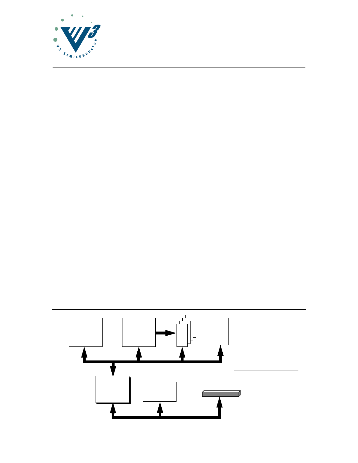
i960Cx/Hx/Jx
CPU
VxxxEPC
LOCAL TO
PCI BRIDGE
Copyright © 1998, V3 Semiconductor Corp. V96BMC Rev D Data Sheet Rev 3.2
V3 Semiconductor reserves the right to change the specifications of this product without notice.
V96BMC and V96xPBC are trademarks of V3 Semiconductor. All other trademarks are the propert
V96BMC
MEMORY
CONTROL
PCI
PERIPHERAL
D
R
A
M
PCI SLOT or EDGE CONNECTOR
ROM
TYPICAL APPLICATION
1
of their respective owners.
V96BMC Rev.D
V3 Semiconductor retains the rights to change documentation, specif ications, or device
functionality at any time without notice. Please verify that you have the latest copy of all
documents before finalizing a design.
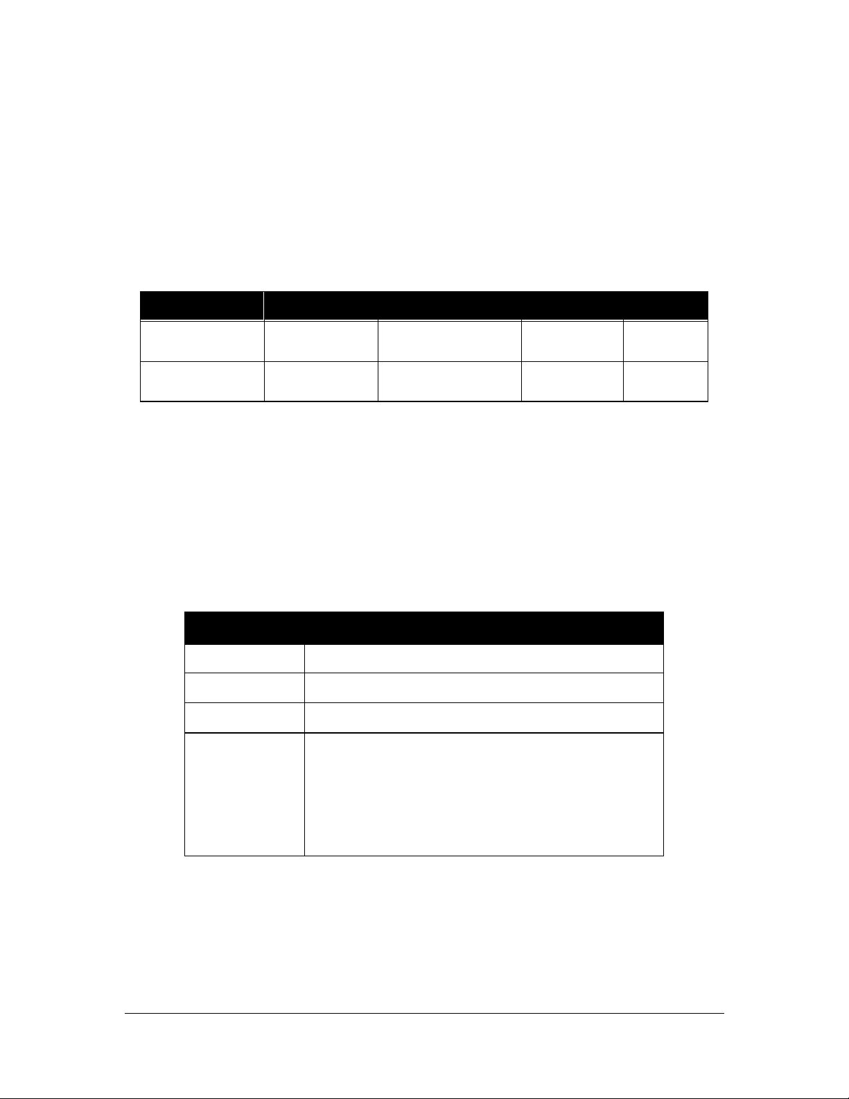
1.0 Product Codes
Table 1: Product Codes
Product Code Processor Bus Type Package Frequency
V96BMC-33LP i960Cx/Hx/Jx
V96BMC-40LP i960Cx/Hx/Jx
32-bit multiplexed /
demultiplexed
32-bit multiplexed /
demultiplexed
132-pin PQFP 33MHz
132-pin PQFP 40MHz
2.0 Pin Description and Pinout
Table 2 below lists the pin types found on the V96BMC. Table 3 describes the function of each pin on
the V96BMC. Table 4 lists the pin s by pin n umber. Figure 1 shows the p inout for the 13 2-pin PQF P
package and Figure 2 shows the mechanical dimensions of the package.
Table 2: Pin Types
Pin Type Description
I/O
12
I TTL input only pin
O
12
TTL I/O pin with 12 mA output drive
TTL Output pin with 12 mA output drive
TTL Output pin with 12 mA output drive that can be
configured for either 5 volt or 3.3 volt signaling, These
outputs can be configured for 3.3V operation by
O
12-3
2
connecting the Vcc3 power pins to a 3.3V power plan e
(Vcc should always be connected to a 5V supply). Vcc3
can also be connected to the 5V plane if 5V signaling is
desired.
V96BMC Rev D Data Sheet Rev 3.2 Copyright © 1998, V3 Semiconductor Inc.
Table 3: Signal Descriptions
Memory Interface Signals
V96BMC Rev.D
Signal Type
AA[11:0]
AB[11:0]
RASA[3:0]
RASB[3:0]
CASA[3:0]
CASB[3:0]
MWEA
MWEB
RFS/AUXT
a
R
Description
Leaf A and B row and column address, multiplexed on the same
O
12-3
X
pins. When non-interleaved operation is select ed, only address bus
AA should be used.
Row Address Strobe. These strobes indicate the presence of a valid
O
12-3
H
row address on busses AA(B)[11:0]. These signals are to be connected one to each 32-bit lea f of memory.
O
12-3
O
12-3
Column Address Strobe. These strobes latch a column address from
H
AA(B)[11:0]. They are assigned one to each byte in a leaf.
Memory Write Enable. These are the DRAM write strobes. One is
H
supplied for eac h leaf to minimize signal loading.
Refresh in progress. This output is multi-function signal. The signal
name, as it appears on the logic symbol, is the default signal names.
O
12
H
This signal gives notice that a refresh cycle is to be executed. The
timing leads RAS only refresh by one cycle. The output may also
function as AUX timer interrupt.
Configuration
Signal Type R Description
HMODE
I Connected to Vcc (for i960Cx) or GND (for i960Hx/Jx).
Buffer Controls Signals
Signal Type R Description
Data Transmit A and B. These outputs are multi-function signals.
The signal names, as they appear on the logic symbol, are the
TXA
TXB
O
12
default signal names (Mode 0). The purpose of these outputs is to
H
control buffer output enables during data read transactions and, in
effect, control the multiplexing of data from each memory leaf onto
the i960Cx/Hx/Jx data bus.
These outputs are mode independent, however, the timing of the
signals chan ge for different operational m odes. They control transLEA
LEB
O
12
parent latche s that hold data t ransmitted during a write transaction.
L
In modes 0 and 1, the latch controls follow the timing of CAS for
each leaf, while in modes 2 and 3 the timing of LEA and LEB is
shortened to 1/2 clock.
Local Bus Interfac e
Copyright © 1998, V3 Semiconductor Corp. V96BMC Rev D Data Sheet Rev 3.2
3
V96BMC Rev.D
Table 3: Signal Descriptions (cont’d)
Signal Type R Description
A[31:2] I Local address bus.
Address Latch Enable: cont rols a set of transparent latches on the
address bus. When asserted high, the address input flows through
ALE I
the latch. When ALE is low, the internal address holds the previous
value. With an i960Cx/Hx processor ALE is not typically used and
has an internal pull-up resistor that will keep it hi gh when not con-
nected (to provide backward pin compatibility with earlier versions).
D/C
I Data/Code.
BE[3:0] I L ocal bus byte write enables.
W/R IWrite/Read.
READY
O
Z Local Bus data ready.
12
ADS I Asserted low to indicate the beginning of a bus cycle
DEN I
SUP I
Data Enable. This input is monitored by the Bus Watch Timer to
detect a bus access not returning READY.
Indicates supervisor mode. Required for access to configuration reg-
isters.
BLAST I Burst last.
BTERM
BERR
O
12
O
12
Burst terminate. (this signal requires a nominal pull up resistor so
Z
that the signal is deasserted when RESET goes inactive)
H Bus Time-out error.
Local interrupt request. This signal is asserted when the 24-bit
INT
O
12
H
counter reaches terminal count, and interrupt out is enabled. May
be programmed for pulse or level operation.
RESET I Local bus reset signal.
PCLK I Local bus clock.
ID[2:0] I These inputs select the address offset of the configuration registers.
Power and Ground Signals
Signal Type R Description
Vcc - POWER leads intended for external connection to a 5V Vcc plane
Vcc3 - POWER for DRAM control outp uts . Ca n b e co nn ect e d to 3. 3V o r 5 V.
GND - GROUND leads intended for external connection to a GND plane.
a. R indicates state during reset.
4
V96BMC Rev D Data Sheet Rev 3.2 Copyright © 1998, V3 Semiconductor Inc.
V96BMC Rev.D
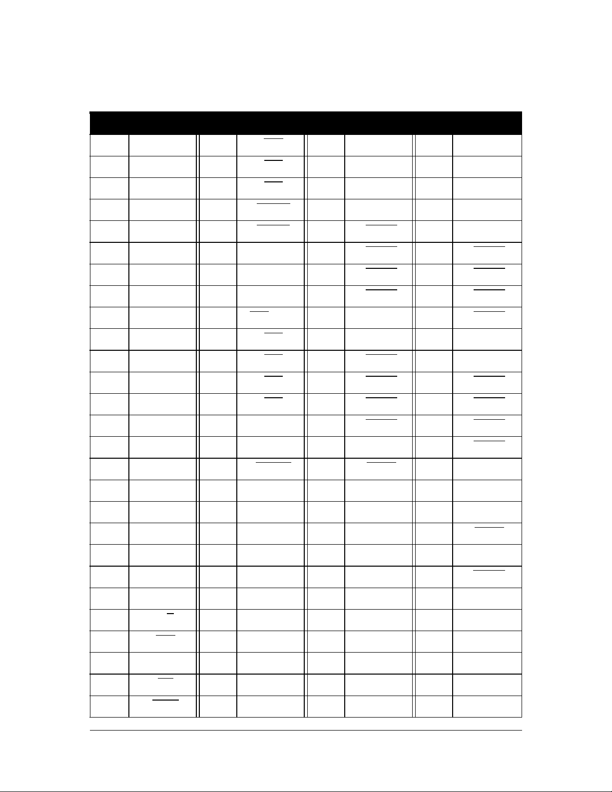
Ta ble 4: Pin Assignments
PIN # Signal PIN # Signal PIN # Signal PIN # Signal
1 A14 34 ADS
2 A15 35 BE2 68 AA11 101 AB10
3 A16 36 BE3 69 Vcc3 102 AB11
4 Vcc 37 BTERM 70 GND 103 Vcc3
5 A17 38 READY 71 CASA 0 104 GND
6 A19 39 ID0 72 CASA1 105 CASB0
7 A20 40 ID1 73 CASA2 106 CASB1
8 A18 41 ID2 74 CASA3 107 CASB2
9 A21 42 RFS/AUXT 75 Vcc3 108 CASB3
10 A24 43 LEA 76 GND 109 Vcc3
11 A22 44 LEB 77 RASA0 110 GND
12 A23 45 TXA 78 R ASA 1 111 RASB0
13 A26 46 TXB 79 R ASA 2 112 RASB1
14 A25 47 Vcc 80 RASA3 113 RASB2
67 AA10 100 AB9
15 A27 48 GN D 81 Vcc3 114 RASB3
16 ALE 49 HMODE 82 MWEA 115 Vcc
17 - 50 - 83 - 116 18 - 51 - 84 - 117
19 A31 52 - 85 - 118 MWEB
20 A28 53 AA0 86 GND 119 GND
21 A29 54 AA1 87 AB0 120 RESET
22 A30 55 AA2 88 AB1 121 A2
23 D/C 56 AA3 89 AB2 122 A3
24 SUP 57 Vcc3 90 AB3 123 A4
25 PCLK 58 GND 91 Vcc3 124 A5
26 INT 59 AA4 92 GND 125 A6
27 BERR 60 AA5 93 AB4 126 A7
GND
1
Copyright © 1998, V3 Semiconductor Corp. V96BMC Rev D Data Sheet Rev 3.2
5

V96BMC Rev.D
Ta ble 4: Pin Assignments (cont’d)
PIN # Signal PIN # Signal PIN # Signal PIN # Signal
28 W/R
29 BE0 62 AA7 95 AB6 128 A9
30 DEN 6 3 Vcc3 96 AB7 129 A10
31 BLAST 64 GND 97 Vcc3 130 A11
32 BE1 65 AA8 98 GND 131 A12
33 GND 66 AA9 99 AB8 132 A13
1. We recommend connecting PIN # 117 to GND but it is not a must especially for those who are
replacing V96BMC rev D in rev AB socket. (This pin was unconnected in rev AB)
61 AA6 94 AB5 127 A8
6
V96BMC Rev D Data Sheet Rev 3.2 Copyright © 1998, V3 Semiconductor Inc.

GND
AB0
AB1
AB2
AB3
VCC3
GND
AB4
AB5
AB6
AB7
VCC3
GND
AB8
AB9
AB10
AB11
VCC3
GND
CASB0#
CASB1#
CASB2#
CASB3#
VCC3
GND
RASB0#
RASB1#
RASB2#
RASB3#
VCC
Figure 1: Pinout for 132-pin PQFP (top view)
MWEA#
VCC3
RASA3#
RASA2#
RASA1#
RASA0#
GND
VCC3
CASA3#
CASA2#
CASA1#
CASA0#
GND
VCC3
AA11
AA10
AA9
AA8
GND
VCC3
AA7
AA6
AA5
AA4
GND
VCC3
AA3
AA2
838281807978777675747372717069686766656463626160595857565554535251
84
85
86
87
88
89
90
91
92
93
94
95
96
97
98
99
100
101
102
103
104
105
106
107
108
109
110
111
112
113
114
115
116
117
118
119
120
121
122
123
124
V96BMC
125
126
127
128
(Top)
Pin #1
IDENT
129
130
131
13212345678910111213141516
V96BMC Rev.D
AA1
AA0
17
50
49
48
47
46
45
44
43
42
41
40
39
38
37
36
35
34
33
32
31
30
29
28
27
26
25
24
23
22
21
20
19
18
HMODE#
GND
VCC
TXB#
TXA#
LEB#
LEA#
RFS#/AUXT
ID2
ID1
ID0
READY#
BTERM#
BE3#
BE2#
ADS#
GND
BE1#
BLAST#
DEN#
BE0#
W/R#
BERR#
INT#
PCLK
SUP#
D/C#
A30
A29
A28
A31
A2A3A4A5A6A7A8
GND
GND
MWEB#
RESET#
Copyright © 1998, V3 Semiconductor Corp. V96BMC Rev D Data Sheet Rev 3.2
A9
A10
A11
A12
A13
A14
A15
A16
VCC
A17
A19
A20
A18
A21
A24
A22
A23
A26
A25
A27
ALE
7

V96BMC Rev.D
Figure 2: 132-pin PQFP mechanical details
0.010 ± 0.002
132+
(0.25 ± 0.05)
1.100 ± 0.003
(27.94 ± 0.08)
0.1675 ± 0.0075
(4.255 ± 0.191)
0.025=(0.800)
32 +
0.64=(20.32)
0.140
(3.57)
0.049 ± 0.007
(1.24 ± 0.18)
132+
0.025 ± 0.003
(0.64 ± 0.08)
1.100 ± 0.003
(27.94 ± 0.08)
0.012 ± 0.004
(0.30 ± 0.10)
1.080 ± 0.005
(27.43 ± 0.13)
132
1
Pin #1
IDENT
0.950 ± 0.003
(24.13 ± 0.08)
0.007 ± 0.001
(0.18 ± 0.03)
0.025 ± 0.005
(0.64 ± 0.13)
0.092 ± 0
(2.34 ± 0)
8
V96BMC Rev D Data Sheet Rev 3.2 Copyright © 1998, V3 Semiconductor Inc.

3.0 DC Specifications
Table 5: Absolute Maximum Ratings
Symbol Parameter Rating Units
V
CC
V
IN
I
IN
T
STG
Symbol Parameter Rating Units
V
CC, VCC3
V
CC3
T
A
Supply voltage -0.3 to +7 V
DC input voltage
DC input current ± 50 mA
Storage temperature -65 to +150 °C
Ta ble 6: Guaranteed Operating Conditions
Supply voltage 4.75 to 5.25 V
Supply voltage for 3.3 Volt DRAM
1
interface
Ambient temperature range 0 to 70 °C
. Vcc is still as above
V96BMC Rev.D
-0.3 to V
3.0 to 3.6 V
CC
+0.3
V
1. For 3.3 Volt DRAM intreface operation.( See also note 8 table 11)
Table 7: DC Operating Specifications Vcc=5Volt and Vcc3=5 Volt
Symbol Description Conditions Min Max Units
V
V
I
IL
I
IH
V
OL
V
OH
I
OZL
I
OZH
I
CC
(max)
C
Low level input voltage Vcc = 4.75V 0.8 V
IL
High level input voltage Vcc = 5.25V 2.0 V
IH
Low level input cur r ent
High level input curr ent
Low level output voltage
High level output voltage
Low level float input
leakage
High level float input
leakage
Maximum supply current
Input and output
IO
capacitance
= GND, V
V
IN
= V
V
IN
= V
V
IN
I
OL
V
= V
IN
I
OL
V
= V
IN
VO = GND
V
= V
IN
VO = 5.25V
Continuous simple access
Continuous burst access
= 5.25V
CC
= 5.25V
CC
IL or VIH
= -12 mA
IL or VIH
= -12 mA
IL or VIH
IL or VIH
-10
-1.0
V
CC
-20
10
0.4 V
20
100
30
20 pF
µ
µ
V
µ
µ
mA
A
A
A
A
Copyright © 1998, V3 Semiconductor Corp. V96BMC Rev D Data Sheet Rev 3.2
9

V96BMC Rev.D
Table 8: DC Operating Specifications Vcc3=3.3 Volt and Vcc=5 Volt
Symbol Description Conditions Min Max Units
V
= Vcc3
V
OL
V
OH
I
OZL
I
OZH
I
CC
(max)
Low level output voltage
High level output voltage
Low level float input
leakage
High level float input
leakage
Maximum supply current
Continuous simple access
Continuous burst access
IN
= 12 mA
I
OL
V
= Vcc3
IN
I
= -12 mA
OL
V
= Vcc2
IN
= GND
VO
= V
V
IN
VO =4.46V
IL or VIH
0.4 V
2.4 V
-10
10
140
40
4.0 AC Specifications
µ
µ
mA
A
A
Table 9: AC Test Conditions
Symbol Parameter Limits Units
Vcc3/Vcc
V
CC3
V
IN
C
OUT
Supply voltage 4.75 to 5.25 V
Supply voltage when 3.3 Volt DRAM inter-
face operation
1
(Vcc is still as above)
3.0 to 3.6 V
Input low and high voltages 0.4 and 4.25 V
Capacitive load on output and I/O pins 50 pF
1. For 3.3 Volt DRAM intreface operation.( See also note 8 table 11)
Table 10: Capacitive Derating for Output and I/O Pins
Output Drive Limit Supply voltage Derating
12 mA Vcc=5 Volt, Vcc3=3.3 Volt 0.06 ns/pF for loads > 50 pF
12 mA Vcc=5 Volt, Vcc3=5 Volt 0.04 ns/pF for loads > 50 pF
10
V96BMC Rev D Data Sheet Rev 3.2 Copyright © 1998, V3 Semiconductor Inc.

V96BMC Rev.D
T able 1 1: T iming Parameters for V96BMC Vcc=5 Volts +/- 5% and Vcc3= 5 or
3.3 8V olts +/- 5%
33 MHz 40 MHz
Symbol Description Note Min Max Min Max Units
PCLK period 30 25 ns
t
C
t
PCLK high time 12 11 ns
CH
t
PCLK low time 12 11 ns
CL
t
Synchronous input setup 9 8 ns
SU
t
Synchronous input hold 1 0.5 ns
H
t
Synchronous input hold (RESET#) 3 3 ns
H
t
READY 3-state to valid delay 1 3 13 3 10 ns
RZH
t
READY synchronous assertion delay 3 13 3 11 ns
RHL
t
READY synchronous de -assertion delay 3 13 3 11 ns
RLH
t
READY valid to 3-state delay 1 3 10 3 7 ns
RHZ
t
BTERM synchronous as sertion delay 3 14 3 12 ns
BHL
t
BTERM synchronous de -assertion del ay 3 13 3 11 ns
BLH
t
BERR synchronous assertion delay 3 13 3 11 ns
EHL
t
BERR synchronous de-assertion de lay 3 12 3 10 ns
ELH
t
INT synchronous assertion delay 3 13 3 11 ns
IHL
t
INT synchronous de-assertion d el ay 3 12 3 10 ns
ILH
t
t
t
t
WESU
ARA1
ARA2
t
RAH
t
CAV
t
CAH
BCAV
t
RHL
t
RLH
t
RAS
t
RSH
t
RP
t
CHL
t
CLH
t
CAS
t
CPN
t
RCD
Address Input to Row Address output delay
314312ns
(Interleaved)
Address Input to Row Address output delay
418415ns
(Non-interleaved)
Row addres s hold from RAS assertion 2 t
MtM
+2 t
MtM
+2 ns
Column address valid from RAS assertion 2 tM+1 tM+4 tM+1 tM+4 ns
Column address hold from CAS assertion t
Column address valid delay from previous
assertion (Burst)
CAS
C
t
C
t
C
ns
+3 tC+3 ns
PCLK to RAS asserted delay 3 13 3 11 ns
PCLK to RAS de-asserted delay 3 13 3 11 ns
RAS pulse width 3 3tC-1 3tC-1 ns
RAS hold from last CAS assertion 4 t
N
t
N
ns
RAS precharge time 5 tP-2 tP-2 ns
PCLK to CAS asserted delay 1 313312ns
PCLK to CAS de-asserted delay 4 12 3 11 ns
CAS pulse width 4 tN-1 tN-1 ns
CAS precharge time 0.5t
RAS to CAS delay time
1.5tC-2
C
1.5t
C
0.5t
1.5tC-2
C
1.5tCns
ns
Write Enable setup to RAS assertion 10 9 ns
Copyright © 1998, V3 Semiconductor Corp. V96BMC Rev D Data Sheet Rev 3.2
11

V96BMC Rev.D
T able 1 1: T iming Parameters for V96BMC Vcc=5 Volts +/- 5% and Vcc3= 5 or
3.3 8V olts +/- 5%
t
t
TXHL1
t
TXHL2
t
t
t
WEH
t
LED
TXLH
RFHL
RFLH
t
ASU
t
AH
Write Enable hold from RAS de-assertion 1313ns
PCLK to Latch Enable out put delay 6 3 12 3 10 ns
PCLK to Buffer Control fall delay 7 3 13 3 11 ns
PCLK to Buffer Control fall delay (Mode 2 and
415413ns
3 at TXA pin only)
PCLK to Buffer Control rise delay 3 12 3 10 ns
REFRESH synchronous assertion delay 3 13 3 11 ns
REFRESH synchronous de-assertion delay 3 13 3 11 ns
Address setup to ALE Falling 6 5 ns
Address hold from ALE Falling 5 4 ns
NOTES:
1. Specified from PCLK falling edge.
= tC when T_MUX = 1; tM = 0.5 • tC when T_MUX = 0.
2. t
M
3. Maximum RAS
= 1.5 • tC when T_RAS = 0; tN = 2.5 • tC when T_RAS = 1.
4. t
N
= 2 • tC when T_RAS = 0; tP = 2 • tC when T_RAS = 1 and T_RP = 1;
5. t
P
= 3 • tC when T_RAS = 1 and T_RP = 0.
t
P
6. Rising delay is measured from PCLK falling edge, falling delay is measured from PCL K rising edge.
7. Except for Mode 2 and 3 at TXA
pulse width depends on the number of burst access.
pin.
8. In order to have 3.3 Volt DRAM interface Vcc3 pins must be connected to 3.3 Volt.
Vcc3 pins are: PIN # 91, 97, 103, 109, 57, 63, 69, 75, 81.
The power supply pins that must always be connected to 5V are Vcc.
Vcc pins are: PIN # 4, 47, 115.
INPUT SETUP/HOLD
OUTPUT FALLING DELAY
OUTPUT RISING DELAY
OUTPUT RISING DELAY
12
Figure 3: Clock and Synchronous Signals
tCH
tHtSU
LOCAL CLOCK
VALID
tLED, BHL, EHL, IHL
,
RFHL, TXHL1, TXHL2
tBLH, ELH, ILH, RFLH
TXLH
V96BMC Rev D Data Sheet Rev 3.2 Copyright © 1998, V3 Semiconductor Inc.
tC
tCL
tLED

ALE
V96BMC Rev.D
Figure 4: ALE Timing
TALE
PCLK
ADS
ADDR
W/R
BLAST
READY
Ax11:0
RASx
CASx
MWEx
A(31:2)
ADDRESS
TASU TAH
Figure 5: Basic Access Timing
012345678
Address N
tRZH
tARA2
tRHL
tWESU tWEH
tRAH
Row
tCAV
tCHL
t
RHL
tRAS
tCAH
Col
tCAS
tRLH
tCLH
tRLH
tRHZ
tRP
tCPNtRCD
Copyright © 1998, V3 Semiconductor Corp. V96BMC Rev D Data Sheet Rev 3.2
13

V96BMC Rev.D
p
PCLK
ADS
ADDR
R/W
BLAST
READY
AA11:0
RASA
CASA
AB11:0
RASB
CASB
LEA
Mode 0, 1
LEB
Mode 0, 1
LEA
Mode 2, 3
LEB
Mode 2, 3
CEA, TXA
CEB, TXB
Figure 6: Burst Access Timing
012345678
Address N
tARA1
tARA1
Row
Col
tBSAV
tLED
tBSAV
Col+2
tRSH
Col+2ColRow
tRSH
tLED
>0 ns
910
5.0 Revision History
Revision
Number
3.2 7/98 V96BMC Rev D timing parameters with 3.3V DRAM support.
3.1 10/96 Data Book revision.
3.0 05/96
2.0 7/92 Updated timings to final A-step values.
1.0 7/92
Date Comments and Changes
Updated timings to final D-step values.
Simplified data sheet format.
First pre-silicon revision of preliminary data sheet.
DC and AC specs TBD. Sent only to a lim ited number of customers
Table 12: Revision Hist ory
Phone: (408)988-1050 Fax: (408)988-2601
Toll Free: (800)488-8410 (Canada and U.S. only)
World Wide Web: htt
USA:
2348G Walsh Ave.
Santa Clara CA 95051
://www.vcubed.com
14
V96BMC Rev D Data Sheet Rev 3.2 Copyright © 1998, V3 Semiconductor Inc.
 Loading...