

V292BMC Rev. D
HIGH PERFORMANCE BURST
DRAM CONTROLLER
FOR Am29030/40 PROCESSORS
• Pin/Software compatible with earlier V292BMC.
• Direct interfaces to Am29030/40 processors.
• 3.3V DRAM interface support.
• Near SRAM performance achieved with DRAM.
• Supports up to 512Mb of DRAM.
• Interleaved or non-interleaved operation.
• Supports symmetric and non-symmetric arrays.
The V292BMC Revision D Burst DRAM
Controller is an enhanced version of the previous
V292BMC with improved timing and provides
dedicated Power and Ground rails to support the
increasingly popular 3.3V DRAM modules.
Timing parameters are also improved over the
older versions of the device.
The V292BMC provides the DRAM access
protocols, buffer signals, data multiplexer
signals, and bus timing resources required to
work with DRAM. By using the V2926BMC,
system designers can replace tedious design
work, expensive FPGAs and valuable board
space with a single, high-performance, easily
configured device. The processor interface of the
V292BMC implements the bus protocol of the
Am29030/40. The pin naming convention has
been duplicated on the V292BMC; simply wire
like-named pins together to create the interface.
The V292BMC supports a total DRAM memory
subsystem size of 512Mbytes. The array may be
• Software-configured operational parameters.
• Integrated Page Cache Management.
• 2Kbyte burst transaction support.
• On chip memory address multiplexer/drivers.
• Two 24-bit timers, 8-bit bus watch timer.
• Up to 40MHz operation.
• Low cost 132-pin PQFP package.
organized as 1 or 2 leafs of 32-bits each.
Standard memory sizes of 256Kbit to 64Mbit
devices are supported and 8, 16, and 32-bit
accesses are allowed. The V292BMC takes
advantage of Fast Page Mode or EDO DRAMs
and row comparison logic to achieve static RAM
performance using dynamic RAMs. Control
signals required for optional external data path
buffers/latches are also provided by the
V292BMC. The V292BMC provides an 8-bit bus
watch timer to detect and recover from accesses
to unpopulated memory regions.Two 24-bit
counters/timers can supply an external interrupt
signal at a constant frequency relative to the
system clock. The V292BMC is packaged in a
low-cost 132-pin PQFP package and is available
in 25, 33, or 40MHz versions.
This document contains the product codes,
pinouts, package mechanical information, DC
characteristics, and AC characteristics for the
V292BMC. Detailed functional information is
contained in the User’s Manual.
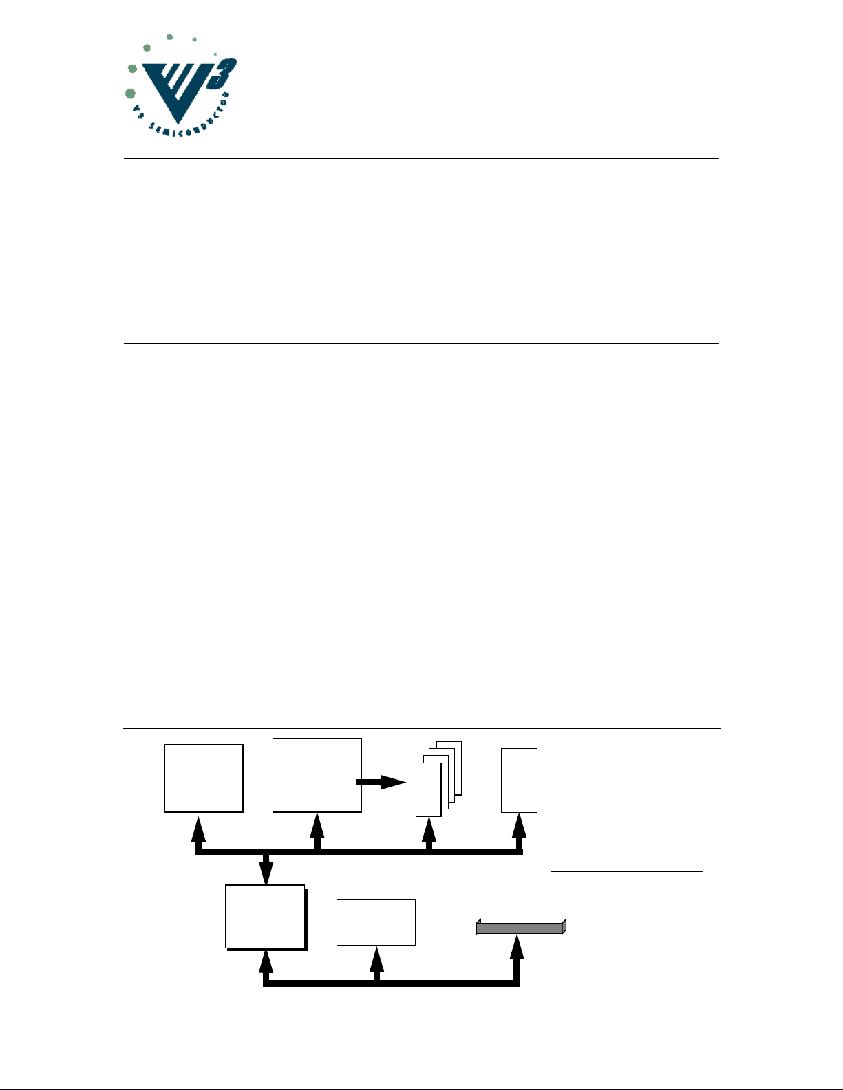
V292BMC
Am29030/40
CPU
MEMORY
CONTROL
D
R
A
M
ROM
TYPICAL APPLICATION
VxxxEPC
LOCAL TO
PCI BRIDGE
Copyright © 1998, V3 Semiconductor Corp. V292BMC Data Sheet Rev 3.2X 1
V3 Semiconductor reserves the right to change the specifications of this product without notice.
V292BMC is trademark of V3 Semiconductor. All other trademarks are the property of their respective owners.
PCI
PERIPHERAL
PCI SLOT or EDGE CONNECTOR
V292BMC Rev.D
V3 Semiconductor retains the rights to change documentation, specifications, or device
functionality at any time without notice. Please verify that you have the latest copy of all
documents before finalizing a design.
1.0 Product Codes
Table 1: Pin Types
Product Code Processor Bus Type Package Frequency
V292BMC-33LP Am29030/35/40 32-bit demultiplexed 132-pin PQFP 33MHz
V292BMC-40LP Am29030/35/40 32-bit demultiplexed 132-pin PQFP 40MHz
2.0 Pin Description and Pinout
Table 2 below lists the pin types found on the V292BMC. Table 3 describes the function of each pin on
the V292BMC. Table 4 lists the pins by pin number. Figure 1 shows the pinout for the 132-pin PQFP
package and Figure 2 shows the mechanical dimensions of the package.
Table 2: Pin Types
Pin Type Description
I/O
12
I TTL input only pin
O
12
O
12-3
TTL I/O pin with 12 mA output drive
TTL Output pin with 12 mA output drive
TTL Output pin with 12 mA output drive that can be
configured for either 5 volt or 3.3 volt signaling, These
outputs can be configured for 3.3V operation by
connecting the Vcc3 power pins to a 3.3V power plane
(Vcc should always be connected to a 5V supply). Vcc3
can also be connected to the 5V plane if 5V signaling is
desired.
2 V292BMC Rev D Data Sheet Rev 3.2 Copyright © 1998, V3 Semiconductor Inc.
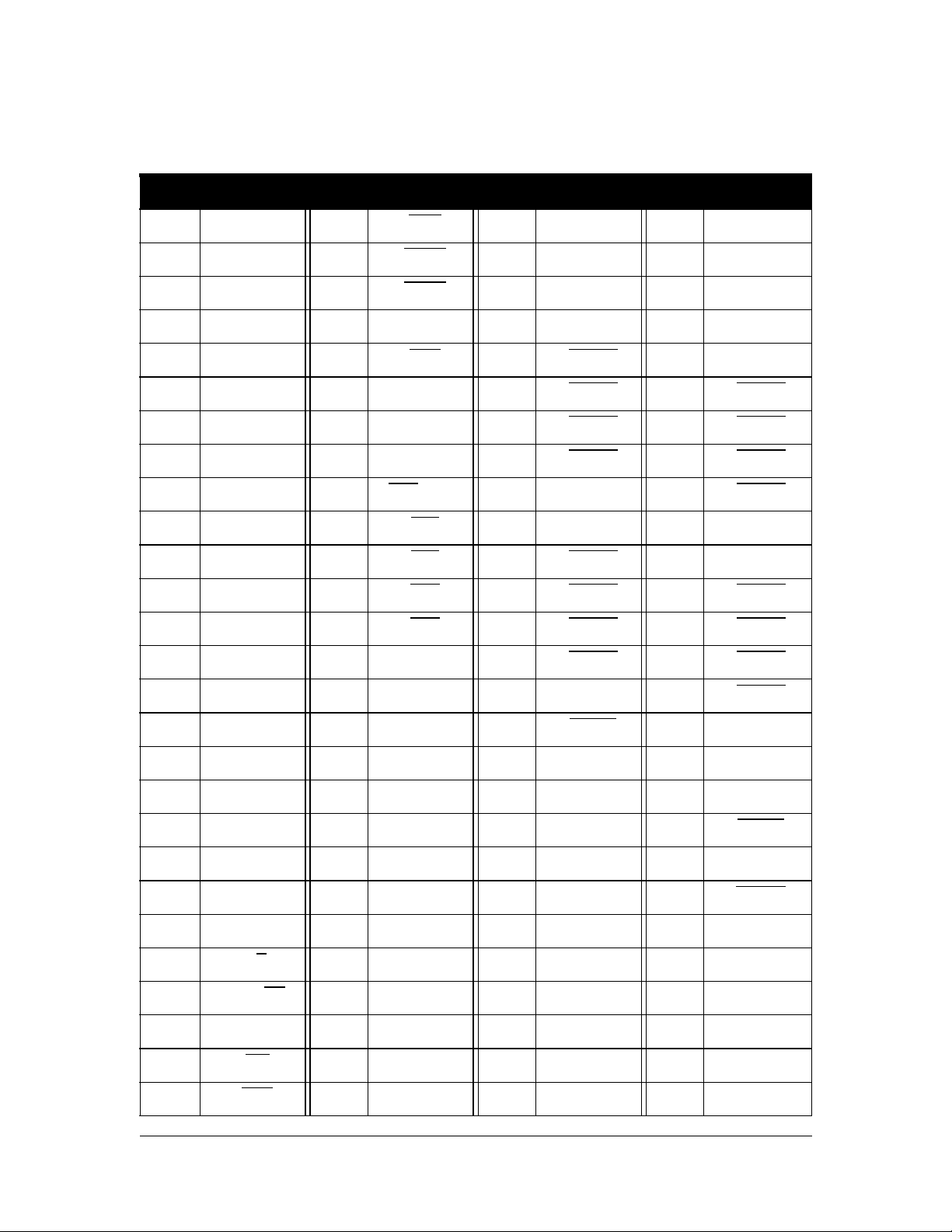
Table 3: Signal Descriptions
Memory Interface Signals
V292BMC Rev.D
Signal Type
AA[11:0]
AB[11:0]
RASA[3:0]
RASB[3:0]
CASA[3:0]
CASB[3:0]
MWEA
MWEB
RFS/AUXT
a
R
Description
Leaf A and B row and column address, multiplexed on the same
O
12-3
X
pins. When non-interleaved operation is selected, only address bus
AA should be used.
Row Address Strobe. These strobes indicate the presence of a valid
O
12-3
H
row address on busses AA(B)[11:0]. These signals are to be connected one to each 32-bit leaf of memory.
O
12-3
O
12-3
Column Address Strobe. These strobes latch a column address from
H
AA(B)[11:0]. They are assigned one to each byte in a leaf.
Memory Write Enable. These are the DRAM write strobes. One is
H
supplied for each leaf to minimize signal loading.
Refresh in progress. This output is multi-function signal. The signal
name, as it appears on the logic symbol, is the default signal names.
O
12
H
This signal gives notice that a refresh cycle is to be executed. The
timing leads RAS only refresh by one cycle. The output may also
function as AUX timer interrupt.
Configuration
Signal Type R Description
MOD4 I Selects Modulo 4 (word) bursting for multiplexed address AA(B).
Buffer Controls Signals
Signal Type R Description
Data Transmit A and B. These outputs are multi-function signals.
The signal names, as they appear on the logic symbol, are the
TXA
TXB
O
12
default signal names (Mode 0). The purpose of these outputs is to
H
control buffer output enables during data read transactions and, in
effect, control the multiplexing of data from each memory leaf onto
the Am29030/40 data bus.
These outputs are mode independent, however, the timing of the
signals change for different operational modes. They control transLEA
LEB
O
12
parent latches that hold data transmitted during a write transaction.
L
In modes 0 and 1, the latch controls follow the timing of CAS for
each leaf, while in modes 2 and 3 the timing of LEA and LEB is
shortened to 1/2 clock.
Local Bus Interface
Copyright © 1998, V3 Semiconductor Corp. V292BMC Rev D Data Sheet Rev 3.2 3
V292BMC Rev.D
Table 3: Signal Descriptions (cont’d)
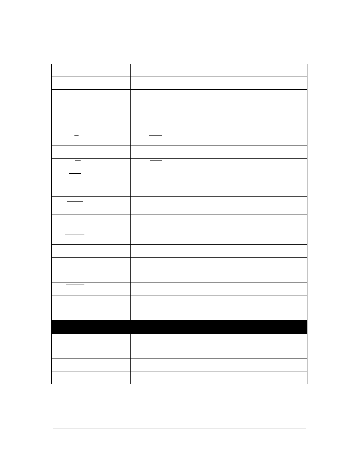
Signal Type R Description
A[31:2] I Local address bus.
Address Latch Enable: controls a set of transparent latches on the
address bus. When asserted high, the address input flows through
ALE I
I/D I Data/Code.
BWE[3:0] I Local bus byte write enables.
R/W I Read/write.
the latch. When ALE is low, the internal address holds the previous
value. With an Am29030/40 processor ALE is not typically used and
has an internal pull-up resistor that will keep it high when not con-
nected (to provide backward pin compatibility with earlier versions).
REQ
RDY
I
O
12
Asserted low to indicate the beginning of a bus cycle.
Z Local bus data ready.
PRDY I Processor ready
SUP/US I
Indicates supervisor mode. Required for access to configuration reg-
isters.
BURST I Burst request.
ERR
O
H Bus Time-out error.
12
Local interrupt request. This signal is asserted when the 24-bit
INT
O
12
H
counter reaches terminal count, and interrupt out is enabled. May
be programmed for pulse or level operation.
RESET I Local bus reset signal.
MEMCLK I Local bus clock.
ID[2:0] I These inputs select the address offset of the configuration registers.
Power and Ground Signals
Signal Type R Description
Vcc - POWER leads intended for external connection to a 5V Vcc plane
Vcc3 - POWER for DRAM control outputs. Can be connected to 3.3V or 5V.
GND - GROUND leads intended for external connection to a GND plane.
a. R indicates state during reset.
4 V292BMC Rev D Data Sheet Rev 3.2 Copyright © 1998, V3 Semiconductor Inc.
V292BMC Rev.D
Table 4: Pin Assignments
PIN # Signal PIN # Signal PIN # Signal PIN # Signal
1 A14 34 REQ 67 AA10 100 AB9
2 A15 35 BWE2 68 AA11 101 AB10
3 A16 36 BWE3 69 Vcc3 102 AB11
4 Vcc 37 GND 70 GND 103 Vcc3
5 A17 38 RDY 71 CASA0 104 GND
6 A19 39 ID0 72 CASA1 105 CASB0
7 A20 40 ID1 73 CASA2 106 CASB1
8 A18 41 ID2 74 CASA3 107 CASB2
9 A21 42 RFS/AUXT 75 Vcc3 108 CASB3
10 A24 43 LEA 76 GND 109 Vcc3
11 A22 44 LEB 77 RASA0 110 GND
12 A23 45 TXA 78 RASA1 111 RASB0
13 A26 46 TXB 79 RASA2 112 RASB1
14 A25 47 Vcc 80 RASA3 113 RASB2
15 A27 48 GND 81 Vcc3 114 RASB3
16 ALE 49 - 82 MWEA 115 Vcc
17 - 50 - 83 - 116 18 - 51 - 84 - 117 MOD4
19 A31 52 - 85 - 118 MWEB
20 A28 53 AA0 86 GND 119 GND
21 A29 54 AA1 87 AB0 120 RESET
22 A30 55 AA2 88 AB1 121 A2
23 I/D 56 AA3 89 AB2 122 A3
24 SUP/US 57 Vcc3 90 AB3 123 A4
25 MEMCLK 58 GND 91 Vcc3 124 A5
26 INT 59 AA4 92 GND 125 A6
27 ERR 60 AA5 93 AB4 126 A7
Copyright © 1998, V3 Semiconductor Corp. V292BMC Rev D Data Sheet Rev 3.2 5

V292BMC Rev.D
Table 4: Pin Assignments (cont’d)
PIN # Signal PIN # Signal PIN # Signal PIN # Signal
28 R/W 61 AA6 94 AB5 127 A8
29 BWE0 62 AA7 95 AB6 128 A9
30 PRDY 63 Vcc3 96 AB7 129 A10
31 BURST 64 GND 97 Vcc3 130 A11
32 BWE1 65 AA8 98 GND 131 A12
33 GND 66 AA9 99 AB8 132 A13
Figure 1: Pinout for 132-pin PQFP (top view)
6 V292BMC Rev D Data Sheet Rev 3.2 Copyright © 1998, V3 Semiconductor Inc.

V292BMC Rev.D
Figure 2: 132-pin PQFP mechanical details
Copyright © 1998, V3 Semiconductor Corp. V292BMC Rev D Data Sheet Rev 3.2 7
V292BMC Rev.D
3.0 DC Specifications
Table 5: Absolute Maximum Ratings
Symbol Parameter Rating Units
V
CC
V
IN
I
IN
T
STG
Symbol Parameter Rating Units
V
CC,VCC3
V
CC3
T
A
Supply voltage -0.3 to +7 V
DC input voltage
DC input current ± 50 mA
Storage temperature -65 to +150 °C
Table 6: Guaranteed Operating Conditions
Supply voltage 4.75 to 5.25 V
Supply voltage for 3.3 Volt DRAM inter-
face operation1. Vcc is still as above
Ambient temperature range 0 to 70 °C
-0.3 to VCC+0.3
3.0 to 3.6 V
V
1. For 3.3 Volt DRAM intreface operation.(See also note 8 table 11)
Table 7: DC Operating SpecificationsVcc=5 Volt and Vcc3=5 Volt
Symbol Description Conditions Min Max Units
V
V
I
IL
I
IH
V
OL
V
OH
Low level input voltage Vcc = 4.75V 0.8 V
IL
High level input voltage Vcc = 5.25V 2.0 V
IH
V
Low level input current
High level input current
Low level output voltage
High level output voltage
= GND, V
IN
V
IN
V
IN
IOL
V
IN
IOL
= V
= V
= V
= 5.25V
CC
= 5.25V
CC
IL or VIH
= -12 mA
IL or VIH
= -12 mA
-10 µA
V
-1.0
CC
10 µA
0.4 V
V
8 V292BMC Rev D Data Sheet Rev 3.2 Copyright © 1998, V3 Semiconductor Inc.

V292BMC Rev.D
Table 7: DC Operating SpecificationsVcc=5 Volt and Vcc3=5 Volt
Symbol Description Conditions Min Max Units
V
V
IOL
VO
IN
VO
IN
VO
V
IOL
V
V
VO
V
= V
IL or VIH
= -GND
= V
IL or VIH
= -5.25V
= Vcc3
IN
= 12 mA
= Vcc3
IN
= -12 mA
= Vcc3
IN
= GND
= Vcc3
IN
=4.465 V
-20 µA
20 µA
100
30
mA
20 pF
0.4 V
2.4 V
-10 µA
10 µA
140
40
mA
I
OZL
I
OZH
I
CC
(max)
C
Low level float input
leakage
High level float input
leakage
Maximum supply current
Input and output
IO
capacitance
Continuous simple access
Continuous burst access
Table 8: DC Operating SpecificationsVcc3=3.3 Volt and Vcc=5 Volt
Symbol Description Conditions Min Max Units
V
OL
V
OH
I
OZL
I
OZH
I
CC
(max)
Low level output voltage
High level output voltage
Low level float input
leakage
High level float input
leakage
Maximum supply current
Continuous simple access
Continuous burst access
4.0 AC Specifications
Table 9: AC Test Conditions
Symbol Parameter Limits Units
V
CC, VCC3
V
CC3
V
IN
C
OUT
1. For 3.3 Volt DRAM interface operation.(See also note 8 table 11)
Copyright © 1998, V3 Semiconductor Corp. V292BMC Rev D Data Sheet Rev 3.2 9
Supply voltage 4.75 to 5.25 V
Supply voltage for 3.3 Volt DRAM inter-
face operation1 (Vcc is still as above)
4.75 to 5.25 V
Input low and high voltages 0.4 and 4.25 V
Capacitive load on output and I/O pins 50 pF
V292BMC Rev.D
Table 10: Capacitive Derating for Output and I/O Pins
Output Drive Limit Supply voltage Derating
12 mA Vcc=5 Volt, Vcc3=3.3 Volt 0.06 ns/pF for loads > 50 pF
12 mA Vcc=5 Volt, Vcc3=5 Volt 0.04 ns/pF for loads > 50 pF
Table 11: Timing Parameters for V292BMC Vcc = 5 Volts +/- 5% and Vcc3 = 5
or 3.38 Volts +/- 5%
33 MHz 40 MHz
Symbol Description Note Min Max Min Max Units
t
MEMCLK period 30 25 ns
C
t
MEMCLK high time 12 11 ns
CH
t
MEMCLK low time 12 11 ns
CL
t
Synchronous input setup 9 8 ns
SU
t
Synchronous input hold 1 0.5 ns
H
t
Synchronous input hold (RESET#) 3 3 ns
H
t
RDY 3-state to valid delay 1 3 13 3 10 ns
RZH
t
RDY synchronous assertion delay 3 13 3 11 ns
RHL
t
RDY synchronous de-assertion delay 3 13 3 11 ns
RLH
t
RDY valid to 3-state delay 1 3 10 3 7 ns
RHZ
t
ERR synchronous assertion delay 3 13 3 11 ns
EHL
t
ERR synchronous de-assertion delay 3 12 3 10 ns
ELH
t
INT synchronous assertion delay 3 13 3 11 ns
IHL
t
INT synchronous de-assertion delay 3 12 3 10 ns
ILH
t
t
t
Address Input to Row Address output delay
ARA1
(Interleaved)
Address Input to Row Address output delay
ARA2
(Non-interleaved)
t
Row address hold from RAS assertion 2 t
RAH
t
Column address valid from RAS assertion 2 tM+1 tM+4 tM+1 tM+4 ns
CAV
t
Column address hold from CAS assertion t
CAH
Column address valid delay from previous
BCAV
CAS assertion (Burst)
t
MEMCLK to RAS asserted delay 3 13 3 11 ns
RHL
t
MEMCLK to RAS de-asserted delay 3 13 3 11 ns
RLH
t
RAS pulse width 3 3tC-1 3tC-1 ns
RAS
t
RAS hold from last CAS assertion 4 t
RSH
t
RAS precharge time 5 tP-2 tP-2 ns
RP
t
MEMCLK to CAS asserted delay 1 3 13 3 12 ns
CHL
3 14 3 12 ns
4 18 4 15 ns
+2 t
MtM
C
tC+3 tC+3 ns
N
MtM
t
C
t
N
+2 ns
ns
ns
10 V292BMC Rev D Data Sheet Rev 3.2 Copyright © 1998, V3 Semiconductor Inc.

V292BMC Rev.D
Table 11: Timing Parameters for V292BMC Vcc = 5 Volts +/- 5% (cont’d)and
Vcc3 = 5 or 3.38 Volts +/- 5%
t
MEMCLK to CAS de-asserted delay 4 12 3 11 ns
CLH
t
CAS pulse width 4 tN-1 tN-1 ns
CAS
t
CAS precharge time 0.5t
CPN
t
RCD
t
WESU
t
WEH
t
LED
t
TXHL1
t
TXHL2
t
TXLH
t
RFHL
t
RFLH
t
ASU
t
AH
RAS to CAS delay time
Write Enable setup to RAS assertion 10 9 ns
Write Enable hold from RAS de-assertion 1 3 1 3 ns
MEMCLK to Latch Enable output delay 6 3 12 3 10 ns
MEMCLK to Buffer Control fall delay 7 3 13 3 11 ns
MEMCLK to Buffer Control fall delay (Mode 2
and 3 at TXA pin only)
MEMCLK to Buffer Control rise delay 3 12 3 10 ns
REFRESH synchronous assertion delay 3 13 3 11 ns
REFRESH synchronous de-assertion delay 3 13 3 11 ns
Address setup to ALE Falling 6 5 ns
Address hold from ALE Falling 5 4 ns
C
1.5tC-2
4 15 4 13 ns
NOTES:
1. Specified from MEMCLK falling edge.
2. tM = tC when T_MUX = 1; tM = 0.5 • tC when T_MUX = 0.
3. Maximum RAS pulse width depends on the number of burst access.
4. tN = 1.5 • tC when T_RAS = 0; tN = 2.5 • tC when T_RAS = 1.
5. tP = 2 • tC when T_RAS = 0; tP = 2 • tC when T_RAS = 1 and T_RP = 1;
tP = 3 • tC when T_RAS = 1 and T_RP = 0.
6. Rising delay is measured from MEMCLK falling edge, falling delay is measured from MEMCLK rising edge.
7. Except for Mode 2 and 3 at TXA pin.
8. In order to have 3.3 Volt DRAM interface Vcc3 pins must be connected to 3.3 Volt.
Vcc3 pins are: PIN # 91, 97, 103, 57, 63, 69, 75, 81.
The power supply pins that must always be connected to 5 Volt are Vcc.
Vcc pins are: PIN # 4, 47, 115.
1.5t
C
0.5t
1.5tC-2
C
1.5tCns
ns
Figure 3: Clock and Synchronous Signals
Copyright © 1998, V3 Semiconductor Corp. V292BMC Rev D Data Sheet Rev 3.2 11

V292BMC Rev.D
Figure 4: ALE Timing
Figure 5: Basic Access Timing
12 V292BMC Rev D Data Sheet Rev 3.2 Copyright © 1998, V3 Semiconductor Inc.
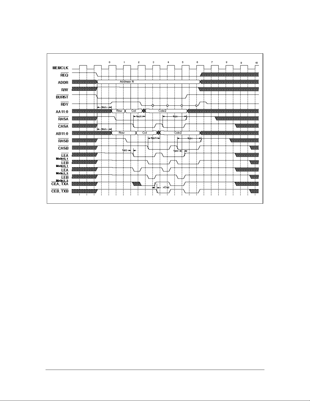
Figure 6: Burst Access Timing
V292BMC Rev.D
Copyright © 1998, V3 Semiconductor Corp. V292BMC Rev D Data Sheet Rev 3.2 13

V292BMC Rev.D
5.0 Revision History
Table 12: Revision History
Revision
Number
3.2 7/98 V292BMC Rev D timing parameters with 3.3V DRAM support.
3.1 10/96 Data Book revision.
3.0 05/96
2.0 7/92 Updated timings to final A-step values.
1.0 7/92
Date Comments and Changes
Updated timings to final D-step values.
Simplified data sheet format.
First pre-silicon revision of preliminary data sheet.
DC and AC specs TBD. Sent only to a limited number of customers
14 V292BMC Rev D Data Sheet Rev 3.2 Copyright © 1998, V3 Semiconductor Inc.
 Loading...