

Page 1

CDMRF101
TCU Phone Module
Component Technical Specification Manual
Ver. 00.1
Apr. 27. 2007
Page 2
Notice
All data and information contained in or disclosed by this document are confidential and
proprietary information of UTStarcom Inc., and all rights therein are expressly reserved.
By accepting this material, the recipient agrees that this material and the information
contained therein are held in confidence and in trust and will not be used, copied,
reproduced, or distributed in whole or in part, nor its contents revealed in any manner
to others without the express written permission of UTStarcom Inc. UTStarcom Inc.
does not assume any liability arising out of the application or use of its products.
UTStarcom Inc. assumes no responsibility for any damage or loss resulting from the
misuse of its products. UTStarcom Inc. assumes no responsibility for any loss or claims
by third parties, which may arise through the use of its products. UTStarcom Inc.
assumes no responsibility for any damage or loss caused by the deletion or loss of data
as a result of malfunctions or repairs. The information contained in this document is
subject to change without notice. Information contained herein is for reference only and
does not constitute a commitment on the part of UTStarcom Inc. Although the
information in this document has been carefully reviewed and it’s believed to be reliable,
UTStarcom Inc. assumes no responsibility or liability for any errors or inaccuracies that
may appear in this document nor are they in anyway responsible for any loss or damage
resulting from the use (or misuse) of this document. It is advised for the customers to
contact our engineers for more information with respect to Keypad, audio interface, RF
interface and input power supply before they start an actual design.
OEM integrators and installers are instructed that the phrase. This device contains
transmitter FCC ID: O6Y-CDMRF101 must be placed on the outside of the host.
Warning: Exposure to Radio Frequency Radiation The radiated output
power of this device is far below the FCC radio frequency exposure
limits. Nevertheless, the device should be used in such a manner that
the potential for human contact during normal operation is minimized.
In order to avoid the possibility of exceeding the FCC radio
frequency exposure limits, human proximity to the antenna should
not be less than 20cm during normal operation. The gain of the
antenna for Cellular band must not exceed 0dBi. The gain of the
antenna for PCS band must not exceed -3dBi.
Page 3

Table of Contents
CDMRF101...........................................................................................................................................................1
TCU PHONE MODULE........................................................................................................................................1
1 INTRODUCTION / OVERVIEW...................................................................................................................6
1.1 MSM 6050 Chipset.................................................................................................................................6
1.1.1 MSM 6050 Features........................................................................................................................6
1.2 IS- Mobile Standards.............................................................................................................................7
1.3 Acronym Definitions..............................................................................................................................8
1.4 Development Tools for the Phone Module..........................................................................................8
1.4.1 LT Box.............................................................................................................................................8
.....................................................................................................................................................................8
2 MECHANICAL DESCRIPTION ...................................................................................................................9
2.1 Phone Module Mechanical Outline ......................................................................................................9
2.2 Phone Module I/O Connector ...............................................................................................................9
2.2.1 I/O Connector Drawing and Supplier Part Number.........................................................................9
2.2.2 I/O Connector Electrical Characteristics.......................................................................................10
2.2.2.1 I/O Connector Pin Assignment..............................................................................................10
3 OPERATING TEMPERATURE AND STORAGE .....................................................................................13
3.1 Temperature.........................................................................................................................................13
3.1.1 Storage Temperature....................................................................................................................13
3.1.2 Operating Temperature.................................................................................................................13
4 ELECTRICAL INTERFACE.......................................................................................................................14
4.1 Design Guidelines ...............................................................................................................................14
4.1.1 Component Derating.....................................................................................................................14
4.1.1.1 Ceramic Capacitors / Parallel Plate Capacitors.....................................................................14
4.1.1.2 Electrolytic Capacitors...........................................................................................................14
4.1.1.3 Tantalum Capacitors..............................................................................................................14
4.1.2 Communication Pins and Unused Pins.........................................................................................14
4.2 Supply Voltage.....................................................................................................................................14
Page 4

4.3 Current Draw........................................................................................................................................15
4.4 Inputs/Outputs Logic Levels ..............................................................................................................15
4.5 Output Power .......................................................................................................................................16
4.6 Audio Interface.....................................................................................................................................16
4.6.1 PCM Audio....................................................................................................................................16
4.6.1.1 MSM Timing Parameters.......................................................................................................16
4.6.1.2 PCM Sync Timing..................................................................................................................16
4.6.1.3 MSM Receive Timing.............................................................................................................17
4.6.1.4 MSM Transmitting Timing......................................................................................................17
4.6.2 UART Data Interface.....................................................................................................................17
4.6.3 Cellular Antenna Open/Short Sense............................................................................................. 19
4.6.4 I/O Interface Circuit Diagrams.......................................................................................................20
Page 5

List of Tables
Page 6

1 INTRODUCTION / OVERVIEW
1.1 MSM 6050 Chipset
The MSM6050 CDMA2000 1X solution is optimized to support voice and key data capabilities while
enabling CDMA2000 network benefits. Designed to support the CDMA2000 1X standard to address
enhanced features as simultaneous voice and data applications and utilize network optimizations, the
MSM6050 chipset will support packet data rates of 153 kbps on the forward and reverse links (FL and RL).
It provides a seamless migration path from 2G to 3G services and applications, and the increased voice
capacity of a CDMA2000 network. The MSM6050 solution will enable manufacturers to quickly develop
handsets meeting specifications for worldwide cdmaOne™ and CDMA2000 1X systems.
The MSM6050 CDMA 2000 1X solution will be used to build a phone module based solution where the
module will be used in a telematics module for an automotive application. The phone module will be
designed for use on the Verizon network. The phone module will not have the typical user interfaces
common to handsets (i.e. keypad, display, etc.). The phone module will have an I/O connector and an RF
connector. Likewise, the phone module will be designed to be certified by Verizon and FCC as a stand
alone module meant for embedded applications.
The MSM6050 chipset solution consists of the MSM6050 baseband processor, direct conversion RFR6155
™ and RFR6000™ receive devices, the direct conversion RFT61500™ transmit device MAX8629™
power management device and a compatible power amplifier device.
1.1.1 MSM 6050 Features
■gpsOne position location capabilities (not enabled in this module)
■CDMA2000 1X support, offering data rates up to 153 kbps on the forward and reverse links
■Quad-mode (CDMA cellular, CDMA PCS, AMPS cellular, gpsOne)
■Vocoder support (EVRC, 13K QCELP)
■Fast 800 Hz forward power control
■Quasi-Orthogonal functions
■Supplemental channel (SCH) support
■CDMA2000 1X Forward Quick Paging channel (F-QPCH)
■Convolutional and turbo codes on SCH
■ITU 144 kbps requirements achieved
■153 kbps on FL and RL (aggregate)
■Integrated wideband mono voice CODEC
Page 7

■Voice recognition (VR) (not enabled in this application)
■Acoustic echo cancellation
■Audio AGC
■External stereo DAC support
■Internal Vocoder supporting 13kbps Pure Voice QCELP and EVRC
■Industry standard ARM7TDMI embedded microprocessor subsystem
■Internal watchdog and sleep timers
■Three universal asynchronous receiver transmitter (UART) serial ports
1.2 IS- Mobile Standards
Standard Description
IS-707 Data Service Options for Spread Spectrum Systems
IS-127 Enhanced Variable Rate Codec (EVRC) EVRC
High Rate Speech Service Option 17 for Wide Band Spread Spectrum
IS-733
Communication Systems
Data Services Option Standard for Wideband Spread Spectrum Digital Cellular
IS-99
System
IS-657 Packet Data Service Option Standard for Wideband Spread Spectrum Systems
Medium Speed Interface for Data Terminal Equipment and Data Circuit Terminating
IS-687
Equipment
Recommended Minimum Standards for 800-MHz Cellular Subscriber
IS-19
Units-Replaced by TIA/EIA-690
The protocol for 'roaming' within the USA, describing how services should 'hand
IS-41
over' between operators
IS-683 Over-the-Air Service Provisioning of Mobile Stations in Spread Spectrum Standards
IS-2000 Introduction to CDMA2000 Spread Spectrum Systems
Comment
13k codec
IS-801 Position Determination Service for cdma2000 Spread Spectrum Systems
Analog Cellular and PCS. The TIA version of the analog cellular standard,
IS-91
IS-95 XXXXXX
incorporating the functionality of IS-88 (narrowband analog) and IS-94 as well
as PCS band operation.
AMPS
Page 8

1.3 Acronym Definitions
Define all acronyms that will be used in the document
1.4 Development Tools for the Phone Module
1.4.1 LT Box
Page 9
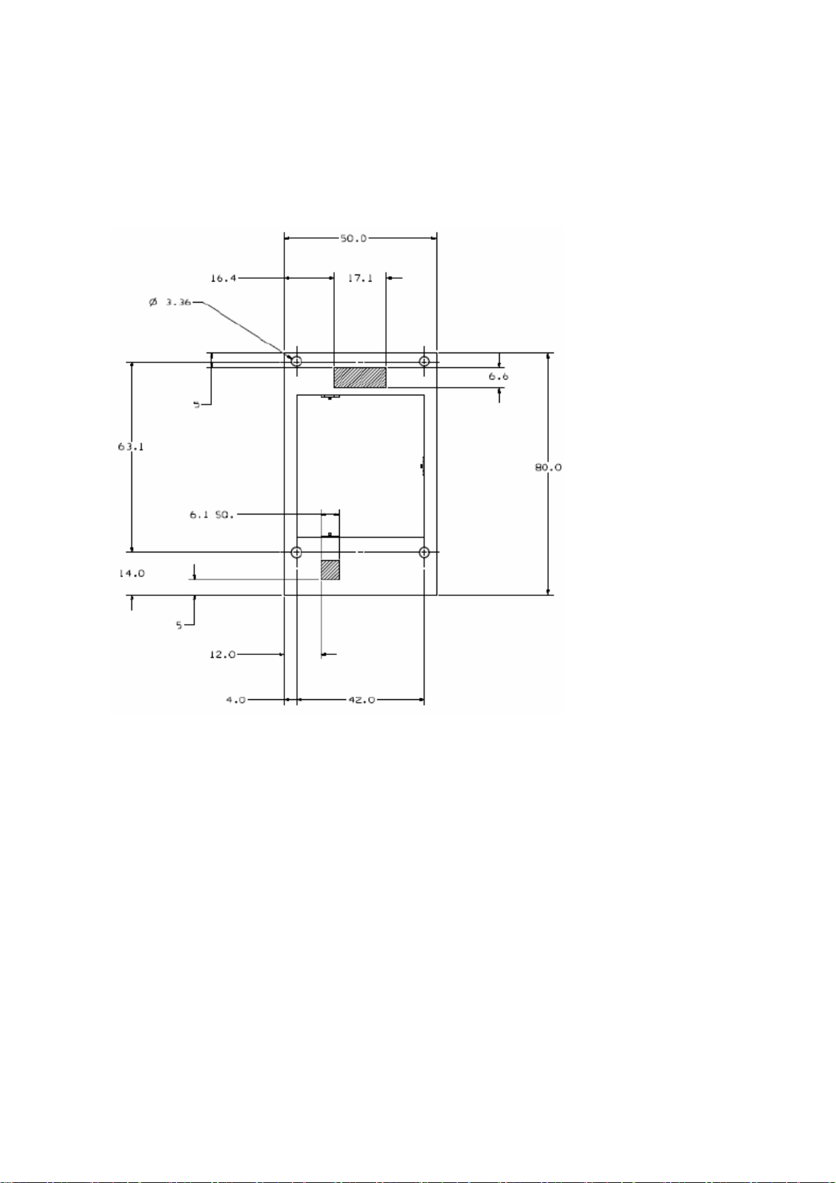
2 MECHANICAL DESCRIPTION
2.1 Phone Module Mechanical Outline
2.2 Phone Module I/O Connector
Iriso 30 pin connector, 9827B-30C-GF
2.2.1 I/O Connector Drawing and Supplier Part Number
This connector is placed on the phone module
Page 10

2.2.2 I/O Connector Electrical Characteristics
I
2.2.2.1 I/O Connector Pin Assignment
Default @
Pin
Name Description
No
1 GND Ground Low O System ground
2 NC NA NA NA NA
3.8 volts +/-5% supply
3 PHONE_PWR
voltage to phone module
Low est
current
mode
High I
I/O @
Phone
Logic Condition
T he application provides the main
power of the phone module
Page 11

4 PHONE_PWR
3.8 volts +/-5% supply
voltage to phone module
High I
T he application provides the main
power of the phone module
5 PHONE_PWR
6 NC NA NA NA NA
7 GND Ground Low O System ground
8 V_REF
9 RI
10 CAIT_RX
11 CAIT_TX
3.8 volts +/-5% supply
voltage to phone module
Reference Logic
Voltage level generated
by the Phone
Ring Indicator
Generated by the phone
CAIT Receive Data
Input to the Phone
CAIT Transmit Data
Output from the Phone
High I
High O
High O
Low I
NA O
T he application provides the main
power of the phone module
Provide the a pplication with its logic
supply
T he phone module indicates the
incoming call condition by pulling down
CAIT RX provides diagnostic signals
from the application to the phone using
AT commands
CAIT TX provides diagnostic signals
from the application to the phone using
the monitor
Ignition indica tor provides the status of
12 IG_IND
13 HW_SD Hardware Shutdown High I
14 SD_REQ
15 PHONE_WU
16 UART_DTR
17 UART_TX
T he Ignition status
indicator
Hardware Shutdown
request
Reuest to wake_up the
phone from TCU
UART Data terminal
ready to Phone from
TCU
UART T ransimt from the
Phone to TCU
High I
High O
High I
High I
Low O
the gnition. Ignition on condition is
indicated by pulling down and ignition off
condition is indicated by pulling up
T he phone module can be shut down by
pulling down
T he phone module can request
hardwarw shutdown by pulling down and
it will be back to pull up after completion
of the hardware shut down
Phone wake up is requested by pulling
down for 500ms
UART DT R provides the status signal
that indicates the TCU processor is
active when it is Low
UART T X provides control signals from
the application to the phone using AT
commands
18 UART_RX UART Recevie to the Low I UART RX provides co signals from the
Page 12

Phone from TCU applic to the phone using AT commands
19 PHONE_RST
20 SPK_OUT_PHO
NE
21 GND Ground Low O System ground
22 MIC_IN_PHONE
23 GND Ground Low O System ground
24 PCM_IN
25 GND GND Low O System ground
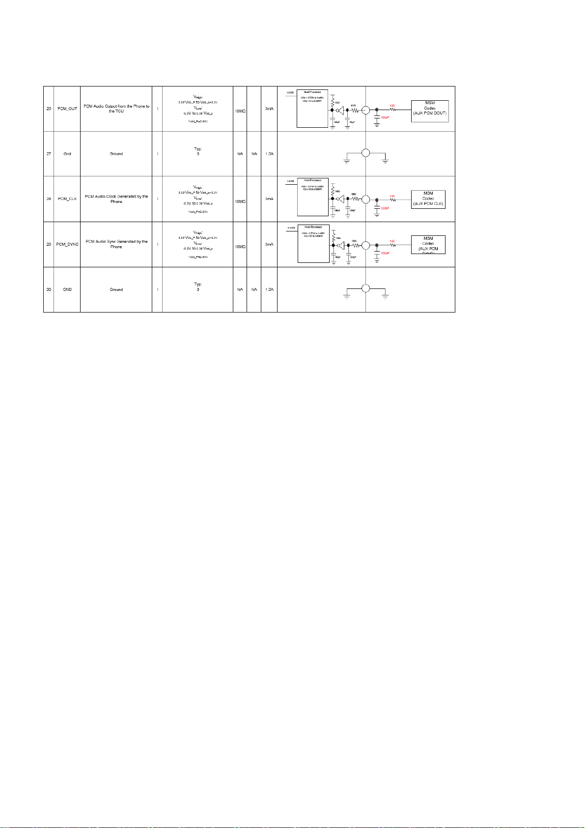
26 PCM_OUT
27 GND GND Low O System ground
Phone Reset gnerated
by the application
Speaker low level audio
Output to TCU from
Phone
Microphone low level
Audio input to Phone
from TCU
PCM Audio Input to the
Phone from TCU
PCM Audio Output from
the Phone to the TCU
High I
TBD O TBD
TBD I TBD
Low I
High O
T he application can reset the phone
module by pulling down
PCM IN provides the and data
information f the TCU application t phone
PCM OUT provides v and data
information f the phone to the appli
28 PCM_CLK
29 PCM _SYNC
30 GND GND Low O System ground
PCM Audio Clock
Low O
Generated by the Phone
PCM Audio Sync
Low O
Generated by the Phone
PCM CLK provides v and data
information f the phone to the appli
PCM sync indicate the signal when it is
high
Page 13

3 OPERATING TEMPERATURE AND STORAGE
3.1 Temperature
3.1.1 Storage Temperature
The phone module shall be capable of being stored at -30C – 85C without any degregation in
performance.
3.1.2 Operating Temperature
The phone module shall operate within specification from -30C – 85C
Page 14

4 ELECTRICAL INTERFACE
Phone / TCU System Mechanization
4.1 Design Guidelines
4.1.1 Component Derating
4.1.1.1 Ceramic Capacitors / Parallel Plate Capacitors
Ceramic capacitors or parallel plate capacitors on power lines shall be two devices in
series to protect against capacitor shorts.
4.1.1.2 Electrolytic Capacitors
Electrolytic capacitors shall be rated at 2x the maximum voltage for a given circuit.
4.1.1.3 Tantalum Capacitors
Tantalum capacitors shall be rated at 3x the maximum voltage for a given circuit on a
power supply. They shall be rated at 2X for applications on signal lines.
Tantalum capacitors shall not be placed on circuits with currents that exceed a current of
1A or the current shall be limited to 1A.
4.1.2 Communication Pins and Unused Pins
Serial communications signals shall be terminated per manufacturers specifications.
Unused IC pins should be terminated according to manufacturer’s recommendations.
4.2 Supply Voltage
Supply Voltage (From TCU to Phone)
Min Max Units
I
Ripple
Max
Max
Page 15

3.8V Supply 3.61 3.99 V 1.0A 100 mV p-p
Regulation type and frequency: Step-down Switching regulator, 220 kHz to 280 kHz
Note: Phone Module should not be damaged by the instantaneous loss of the supply voltage
4.3 Current Draw
Current Draw Chart @ Room Temperature 25C
Current @ 5.0V Duration Period
CDMA: 0 dBW Call
CDMA: -7 dBW Call
CDMA: Verizon Slot cycle index for
waiting for incomming call
CDMA Registration
Phone Mode
Wake 90 110 130 mA 130 ms
Sleep
Pre-Wake up
Wake up
Min Typ Max Units Min Typ Max Units Min Typ Max Units
NA NA NA uA NA NA NA us NA NA NA us
800 mA NA NA NA us NA NA NA us
600 800 uA
150
800
mA
mA us
5.12-
wakeuptime
s
20
s
us
min
4.4 Inputs/Outputs Logic Levels
Parameter
Voltage Output High VOH 2.437 3.187
Voltage Output Low VOL 0.00 0.45
Voltage Input High VIH 1.87655 3.187
Limits
Min Max Units
Volts
Volts
Volts
Page 16

Voltage Input Low VIL -0.3 1.01045
Volts
4.5 Output Power
The phone output power is measured at the end of phone module antenna connector using the RF power
meter. The power level of the phone module is controlled by the base station and the range of the power
level is varied from Min output power to Max output power that is defined in the table below.
Item Specification Min Typical Maximum Unit
Max Output Power Power Class II 23 24 26 dBm/1.23MHz
Min Output Power -53 -50 dBm/1.23MHz
4.6 Audio Interface
4.6.1 PCM Audio
4.6.1.1 MSM Timing Parameters
4.6.1.2 PCM Sync Timing
Page 17

4.6.1.3 MSM Receive Timing
4.6.1.4 MSM Transmitting Timing
4.6.2 UART Data Interface
The Universal Asynchronous Receiver Transmitter (UART) communicates with serial data that
conforms to RS-232 interface protocol. The UART can be used as a serial data port
in Mobile Station testing and debugging with a properly written, user-defined download program.
All communication between the microprocessor and the UART goes through the microprocessor
interface. The microprocessor interface synchronizes the data and command signals to the UART.
Page 18

The UART has a 512-byte transmit FIFO and a 512-byte receive FIFO.
UART1 (CAIT_RX, CAIT_TX) Mobile Station Test, Debugging, Download
UART2 (UART_RX, UART_TX)
Communication between the Phone Module and
TCU
The phone shall have the following UART parameters set by default.
Baud = 9600
Data Bits = 8
Parity = ODD
Stop Bit = 1
Start Bit = 1
Flow Control = None
Line feed and Carriage return shall be sent following each command and re sponse.
Page 19

4.6.3 Cellular Antenna Open/Short Sense
The phone module provides the antenna diagnostics function by the antenna detection circuit. The
antenna detection circuit can detect three statuses: GOOD, OPEN and SHORTED. The detection circuit
can support the antenna resistance values of 1 kOhm to 20 kOhm. The commands are detailed in the AT
command manual.
DC Voltage 2.60V
Status ADC Voltage HEX
GOOD 1.30V 0x80
OPEN 2.60V 0xFF
SHORTED 0.00V 0x00
PAM
LNA
TX
Path
RX
Path
Duplexer
Antenna
DC
10K
Voltage
Detector
10KDNI
MSM
Page 20

4.6.4 I/O Interface Circuit Diagrams
Page 21

Page 22
 Loading...