

Page 1
Rev. 1.4
UTRON
8K X 8 BIT LOW POWER CMOS SRAM
UT6264C
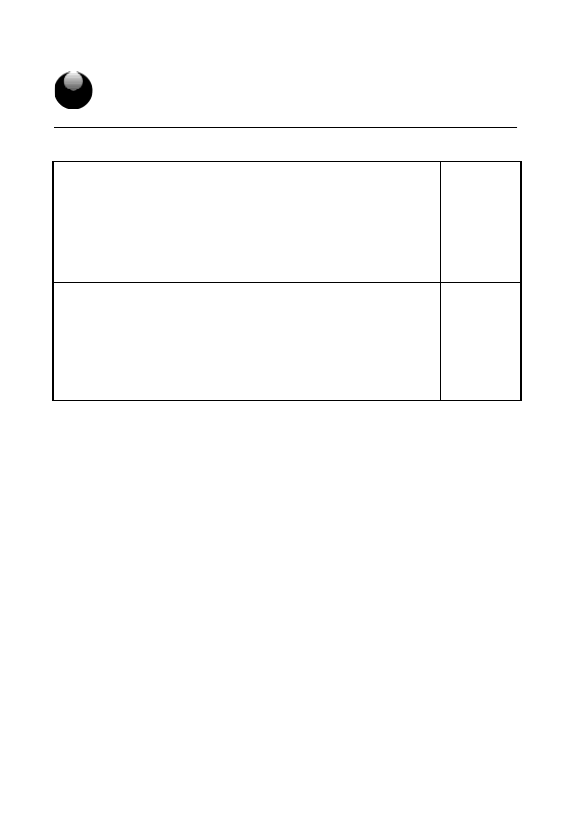
REVISION HISTORY
REVISION DESCRIPTION Date
Preliminary Rev. 0.1 Original. May 3 ,2001
Rev. 1.0
Rev. 1.1
Rev. 1.2
Rev. 1.3
Rev. 1.4 Add order information for lead free product May 15,2003
Revised
-
The timeing waveforms add CE2 control pin
Revised
-
Package outline dimension
-
Waveform.
Revised
-
Improve I
-
28-pin PDIP package outline dimension
1. Add Extended temperature : -20℃~85℃
2. Revised Operating : 45/30 mA (typ.)40/30 mA (typ.)
3. Revised CMOS Standby : 20.3mA (typ.) normal
4. Revised DC characteristics :
a. Icc(-35) : 4540mA (typ.), 6050 mA (max)
b. Icc(-70) : 4540mA (max.)
c. Icc1(Tcycle=1us)= 10mA(max.)
d. Icc2(Tcycle=500ns)=20mA(max.)
5. Revised “Order information” : add Extended parts
from 20µA to 10µA (LL-version , max.)
DR
Jun.4,2001
Jan 15,2002
May 14,2002
Jul 30,2002
UTRON TECHNOLOGY INC. P80028
1F, No. 11, R&D Rd. II, Science-Based Industrial Park, Hsinchu, Taiwan, R. O. C.
TEL: 886-3-5777882 FAX: 886-3-5777919
1
Page 2

Page 3
Rev. 1.4
UTRON
FEATURES
Access time : 35/70ns (max.)
Low power consumption :
Operating : 40/30 mA (typ.)
CMOS Standby : 0.3mA (typ.) normal
2 µA (typ.) L-version
1 µA (typ.) LL-version
Single 4.5V~5.5V power supply
Operating temperature :
Commercial : 0℃~70℃
Extended : -20℃~85℃
All inputs and outputs TTL compatible
Fully static operation
Three state outputs
Data retention voltage : 2V (min.)
Package : 28-pin 600 mil PDIP
28-pin 330 mil SOP
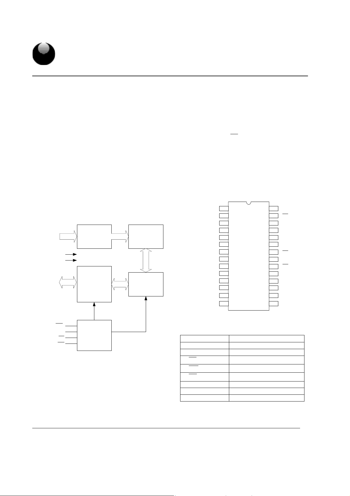
FUNCTIONAL BLOCK DIAGRAM
A0-A12
I/O1-I/O8
DECODER
Vcc
Vss
I/O DATA
CIRCUIT
8K X 8
MEMORY
ARRAY
COLUMN I/O
UT6264C
8K X 8 BIT LOW POWER CMOS SRAM
GENERAL DESCRIPTION
The UT6264C is a 65,536-bit low power CMOS static
random access memory organized as 8,192 words by
8 bits. It is fabricated using high performance, high
reliability CMOS technology.
Easy memory expansion is provided by using two
chip enable input.(
,CE2) ,and supports low data
CE
retention voltage for battery back-up operation with
low data retention current.
The UT6264C operates from a single 4.5V~5.5V
power supply and all inputs and outputs are fully TTL
compatible.
PIN CONFIGURATION
NC
A12
A7
A6
A5
A4
A3
A2
A1
A0
I/O1
I/O2
I/O3
Vss
1
2
3
4
UT6264C
5
6
7
8
9
10
11
12
13
14
28
27
26
25
24
23
22
21
20
19
18
17
16
15
Vcc
WE
CE2
A8
A9
A11
OE
A10
CE
I/O8
I/O7
I/O6
I/O5
I/O4
PDIP/SOP
CE
CE2
OE
WE
CONTROL
CIRCUIT
PIN DESCRIPTION
SYMBOL DESCRIPTION
A0 - A12 Address Inputs
I/O1 - I/O8 Data Inputs/Outputs
,CE2
CE
WE
OE
VCC Power Supply
VSS Ground
NC No connection
Chip Enable Inputs
Write Enable Input
Output Enable Input
UTRON TECHNOLOGY INC. P80028
1F, No. 11, R&D Rd. II, Science-Based Industrial Park, Hsinchu, Taiwan, R. O. C.
TEL: 886-3-5777882 FAX: 886-3-5777919
2
Page 4
Rev. 1.4
UTRON
8K X 8 BIT LOW POWER CMOS SRAM
UT6264C
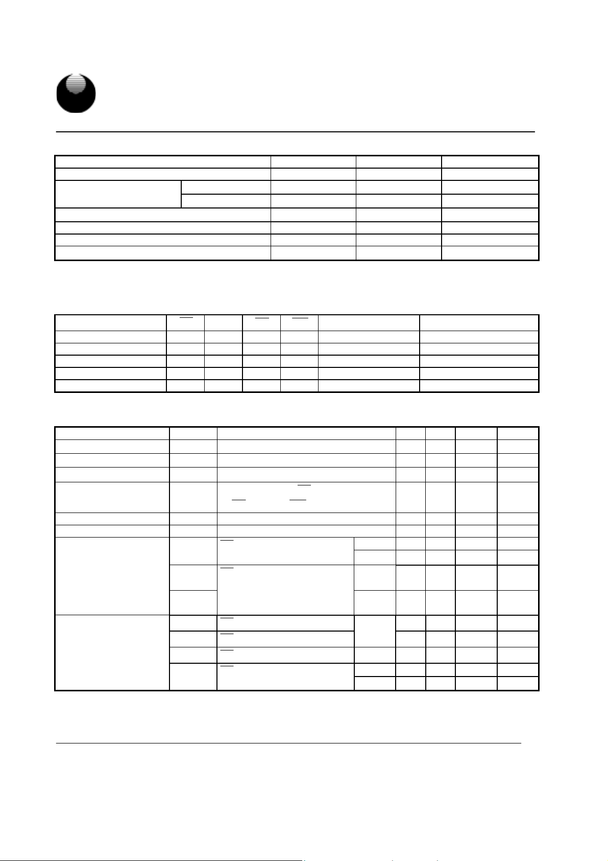
ABSOLUTE MAXIMUM RATINGS*
PARAMETER SYMBOL RATING UNIT
Terminal Voltage with Respect to VSS V
Operating Temperature
Commercial TA 0 to 70
Extended
T
Storage Temperature T
Power Dissipation PD 1 W
DC Output Current I
Soldering Temperature (under 10 sec) Tsolder 260
*Stresses greater than those listed under “Absolute Maximum Ratings” may cause permanent damage to the device. This is a stress rating
only and functional operation of the device or any other conditions above those indicated in the operational sections of this specification is
not implied. Exposure to the absolute maximum rating conditions for extended period may affect device reliability.
TRUTH TABLE
MODE
CE2
CE
OE
Standby H X X X High - Z ISB, ISB1
Standby X L X X High - Z ISB, ISB1
Output Disable L H H H High - Z Icc,Icc1,Icc2
Read L H L H
Write L H X L
note: H = VIH, L=VIL, X = Don't care.
DC ELECTRICAL CHARACTERISTICS
PARAMETER SYMBOL TEST CONDITION MIN. TYP. MAX. UNIT
Input High Voltage
Input Low Voltage
Input Leakage Current
Output Leakage Current I
Output High Voltage V
Output Low Voltage V
Operating Power
Supply Current
Standby Power
Supply Current
V
IH
V
IL
I
LI
LO
OH
OL
I
CC
Icc1
Icc2
I
SB
I
SB1
I
SB
I
SB1
1
*
*
2
≦
V
SS
≦
V
SS
or OE= V
I
= -1mA
OH
I
= 4mA
OL
= V
CE
= 0mA ,Cycle=Min.
I
I/O
= 0.2V; I
CE
CE2=Vcc-0.2V;
other pins at 0.2V or V
CE
CE
CE
CE
=V
≧
=V
≧
(VCC = 4.5V~5.5V, TA = 0℃ to 70℃/-20℃ to 85℃(E))
≦
V
VCC
IN
≦
V
V
I/O
;
or
IH
,
IL
I/O
or CE2= V
IH
-0.2V
V
CC
or CE2= V
IH
V
-0.2V
CC
Notes:
1. Overshoot : Vcc+2.0v for pulse width less than 10ns.
2. Undershoot : Vss-2.0v for pulse width less than 10ns.
3. Overshoot and Undershoot are sampled, not 100% tested.
UTRON TECHNOLOGY INC. P80028
1F, No. 11, R&D Rd. II, Science-Based Industrial Park, Hsinchu, Taiwan, R. O. C.
TEL: 886-3-5777882 FAX: 886-3-5777919
-0.5 to 7.0 V
TERM
℃
-20 to 85
A
-65 to 150
STG
50 mA
OUT
℃
℃
℃
I/O OPERATION SUPPLY CURRENT
WE
=V
CC;
WE
= 0mA;
or CE2≦ 0.2V
or CE2≦ 0.2V
CE
IL
3
IL
= V
CC
IH;
IL
-0.2V
D
OUT
D
IN
Icc,Icc1,Icc2
Icc,Icc1,Icc2
2.2 - V
+0.5 V
CC
- 0.5 - 0.8 V
A
µ
A
µ
or CE2=V
- 1 - 1
IL;
- 1 - 1
2.4 - - V
- - 0.4 V
- 35 - 40 50 mA
- 70 - 30 40 mA
Tcycle
- - 10 mA
=1µs
Tcycle
- - 20 mA
=500ns
normal
- 1 10 mA
0.3 5 mA
-L/-LL - - 3 mA
-L - 2 100
-LL - 1 50
A
µ
A
µ
Page 5
UTRON
Rev. 1.4
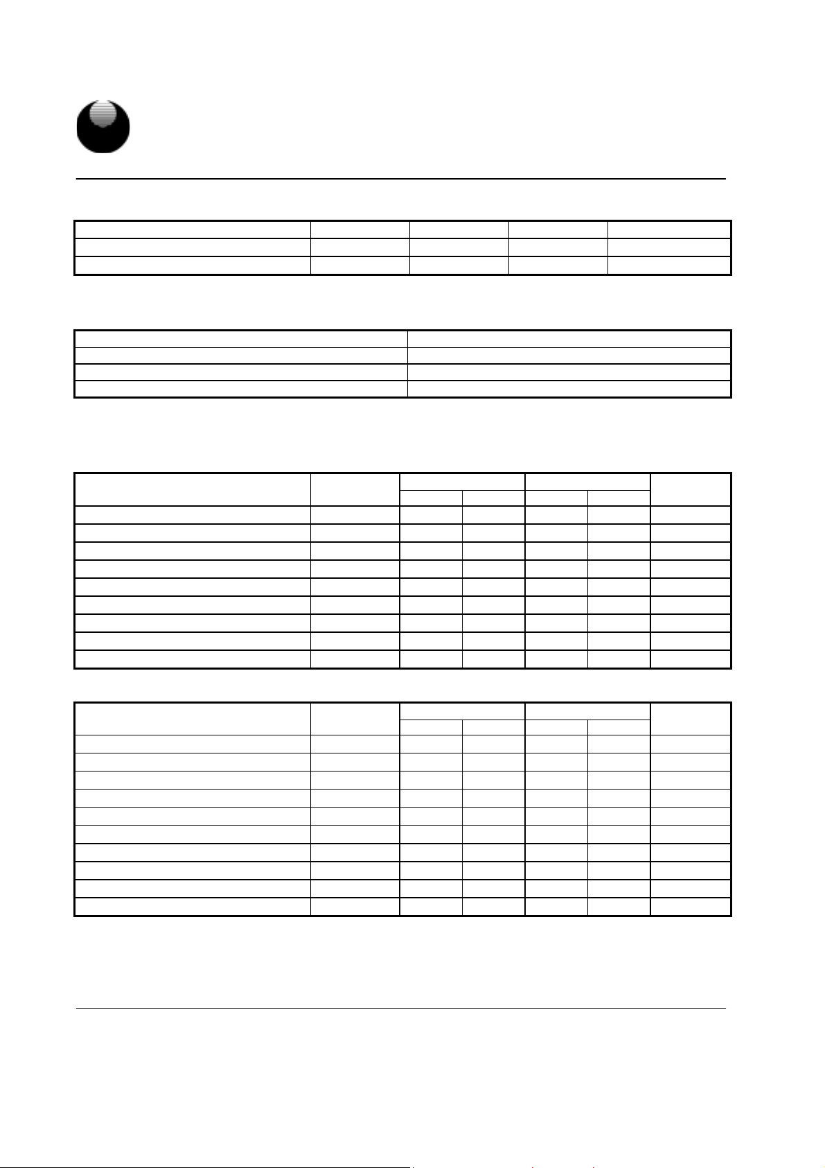
CAPACITANCE
PARAMETER SYMBOL MIN. MAX UNIT
Input Capacitance C
Input/Output Capacitance C
Note : These parameters are guaranteed by device characterization, but not production tested.
AC TEST CONDITIONS
Input Pulse Levels 0V to 3.0V
Input Rise and Fall Times 5ns
Input and Output Timing Reference Levels 1.5V
Output Load CL = 100pF, IOH/IOL = -1mA/4mA
(TA=25℃, f=1.0MHz)
8K X 8 BIT LOW POWER CMOS SRAM
IN
I/O
-
-
8 pF
10 pF
UT6264C
AC ELECTRICAL CHARACTERISTICS
(V
= 4.5V~5.5V, TA = 0℃ to 70℃/-20℃ to 85℃(E))
CC
(1) READ CYCLE
PARAMETER
Read Cycle Time
Address Access Time
Chip Enable Access Time
Output Enable Access Time
Chip Enable to Output in Low-Z
Output Enable to Output in Low-Z
Chip Disable to Output in High-Z
Output Disable to Output in High-Z
Output Hold from Address Change
(2) WRITE CYCLE
PARAMETER SYMBOL
Write Cycle Time
Address Valid to End of Write
Chip Enable to End of Write
Address Set-up Time
Write Pulse Width
Write Recovery Time
Data to Write Time Overlap
Data Hold from End of Write-Time
Output Active from End of Write
Write to Output in High-Z
*These parameters are guaranteed by device characterization, but not production tested.
SYMBOL
tRC 35 - 70 - ns
tAA - 35 - 70 ns
t
- 35 - 70 ns
ACE
tOE - 25 - 35 ns
t
10 - 10 - ns
CLZ*
t
5 - 5 - ns
OLZ*
t
- 25 - 35 ns
CHZ*
t
- 25 - 35 ns
OHZ*
tOH 5 - 5 - ns
tWC 35 - 70 - ns
tAW 30 - 60 - ns
tCW 30 - 60 - ns
tAS 0 - 0 - ns
tWP 25 - 50 - ns
tWR 0 - 0 - ns
tDW 20 - 30 - ns
tDH 0 - 0 - ns
t
5 - 5 - ns
OW*
t
- 15 - 25 ns
WHZ*
UT6264C-35 UT6264C-70
MIN. MAX. MIN. MAX.
UT6264C-35 UT6264C-70
MIN. MAX. MIN. MAX.
UNIT
UNIT
UTRON TECHNOLOGY INC. P80028
1F, No. 11, R&D Rd. II, Science-Based Industrial Park, Hsinchu, Taiwan, R. O. C.
TEL: 886-3-5777882 FAX: 886-3-5777919
4
Page 6
UTRON
Rev. 1.4
TIMING WAVEFORMS
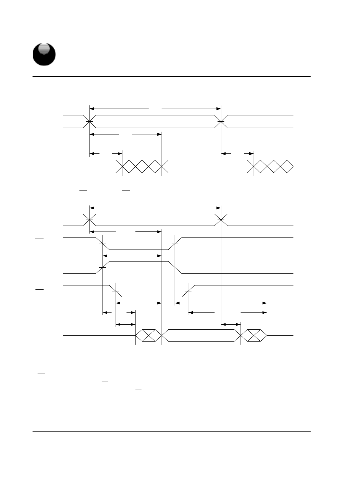
READ CYCLE 1
Address
Dout
READ CYCLE 2
Address
(Address Controlled)
Previous data valid
(CEand
CE2
8K X 8 BIT LOW POWER CMOS SRAM
(1,2)
RC
t
AA
t
OH
t
Data Valid
and
OE
AA
t
Controlled)
t
(1,3,4,5)
RC
t
OH
UT6264C
CE
tACE
CE2
OE
CHZ
OLZ
.
t
tOHZ
t
OH
OE
t
tCLZ
OLZ
t
Dout
Notes :
1.
is high for read cycle.
WE
2.Device is continuously selected
3.Address must be valid prior to or coincident withCE=low, CE2=high; otherwise tAA is the limiting parameter.
, t
, t
OLZ
CHZ
and t
4.t
CLZ
5.At any given temperature and voltage condition, t
High-Z
=low,CE=low, CE2=high
OE
are specified with CL=5pF. Transition is measured±500mV from steady state.
OHZ
is less than t
CHZ
.
CLZ
, t
OHZ
Data Valid
is less than t
High-Z
UTRON TECHNOLOGY INC. P80028
1F, No. 11, R&D Rd. II, Science-Based Industrial Park, Hsinchu, Taiwan, R. O. C.
TEL: 886-3-5777882 FAX: 886-3-5777919
5
Page 7
UTRON
Rev. 1.4
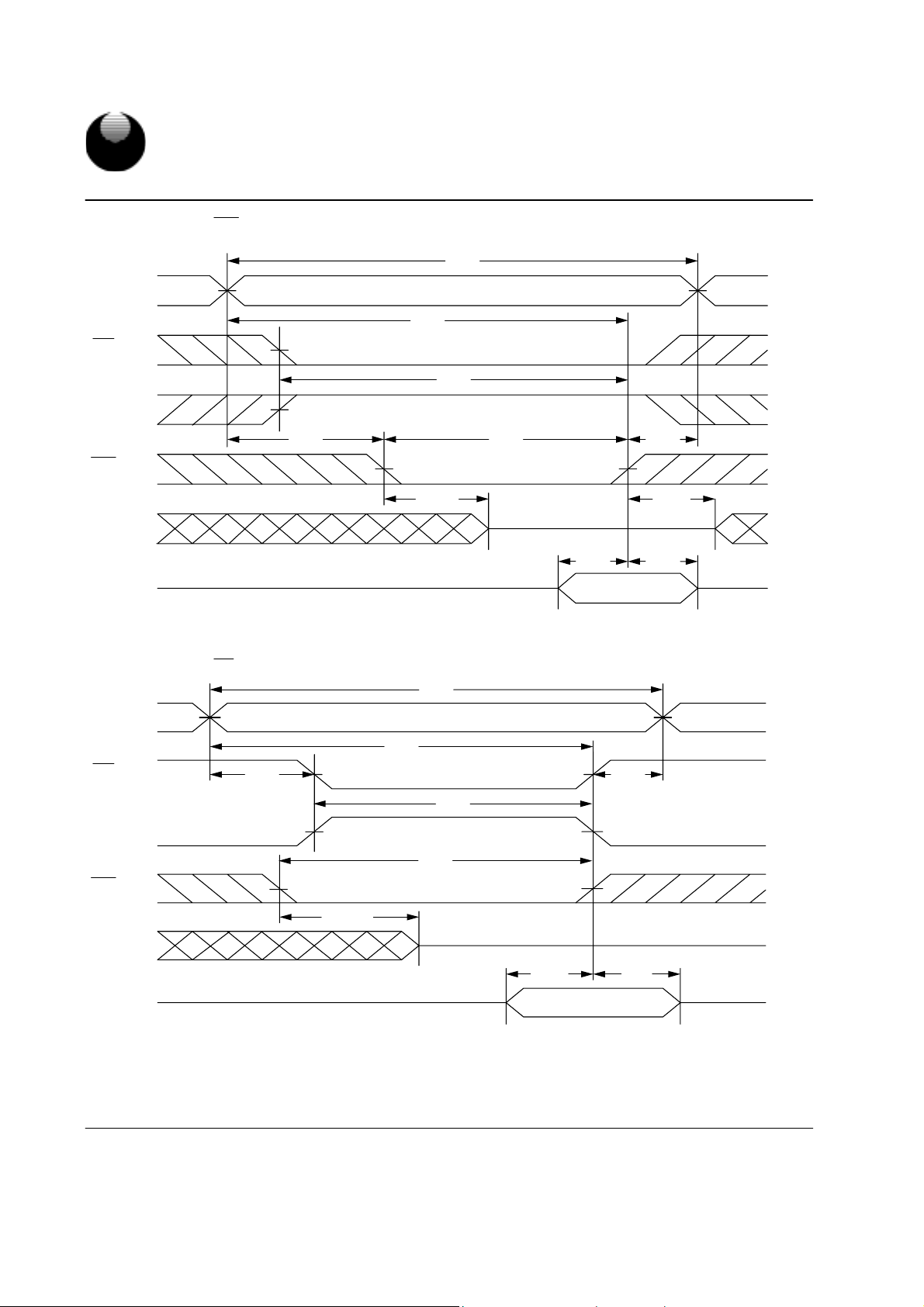
WRITE CYCLE 1
Address
CE
CE2
WE
Dout
Din
(
WE
8K X 8 BIT LOW POWER CMOS SRAM
Controlled)
(1,2,3,5,6)
t
AS
t
WC
AW
t
CW
t
t
WP
WHZ
t
(4) (4)
High-Z
t
DW
Da ta Valid
UT6264C
t
WR
OW
t
t
DH
WRITE CYCLE 2
Address
CE
CE2
WE
Dout
Din
(CEand CE2 Controlled)
t
AS
t
WHZ
(4)
(1,2,5,6)
t
AW
t
t
WC
WP
t
WR
t
CW
High-Z
t
DW
Data V a lid
t
DH
UTRON TECHNOLOGY INC. P80028
1F, No. 11, R&D Rd. II, Science-Based Industrial Park, Hsinchu, Taiwan, R. O. C.
TEL: 886-3-5777882 FAX: 886-3-5777919
6
Page 8
Rev. 1.4
UTRON
8K X 8 BIT LOW POWER CMOS SRAM
UT6264C
Notes :
1.
,CEmust be high or CE2 must be low during all address transitions.
WE
2.A write occurs during the overlap of a low
3. During a
the bus.
4.During this period, I/O pins are in the output state, and input signals must not be applied.
5. If the
impedance state.
6.t
and t
OW
controlled write cycle with
WE
low transition and CE2 high transition occurs simultaneously with or afterWElow transition, the outputs remain in a high
CE
are specified with CL = 5pF. Transition is measured ±500mV from steady state.
WHZ
, high CE2, lowWE.
CE
must be greater than t
low, t
OE
WP
WHZ+tDW
to allow the drivers to turn off and data to be placed on
DATA RETENTION CHARACTERISTICS
(TA = 0℃ to 70℃/-20℃ to 85℃(E))
PARAMETER SYMBOL TEST CONDITION MIN. TYP. MAX. UNIT
Vcc for Data Retention
Data Retention Current
Chip Disable to Data
Retention Time
Recovery Time
t
= Read Cycle Time
RC*
V
I
t
CDR
DR
DR
t
R
≧
V
-0.2V or CE2 ≤ 0.2V
CE
Vcc=2V
CE
CC
≧
V
-0.2V or CE2 ≤ 0.2V
CC
-L - 1 50
-LL - 0.5 10
See Data RetentionWaveforms
(below)
t
2.0 - 5.5 V
0 - - ns
RC*
- - ns
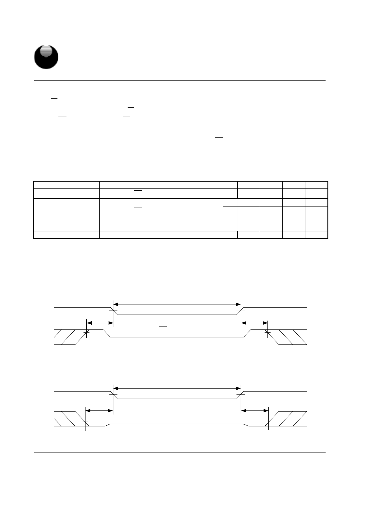
DATA RETENTION WAVEFORM
Low Vcc Data Retention Waveform (1)
(CE controlled)
µA
A
µ
VDR ≧ 2V
CC
V
CE
cc(min.)
V
V
CDR
t
cc(min.)
V
R
t
≧
CE
VCC-0.2V
IH
IH
V
Low Vcc Data Retention Waveform (2)
(CE2 controlled)
VDR ≧ 2V
CC
V
CE2
CC(min.)
V
t
V
CDR
IL
CE2 ≦ 0.2V
CC(min.)
V
t
R
V
IL
UTRON TECHNOLOGY INC. P80028
1F, No. 11, R&D Rd. II, Science-Based Industrial Park, Hsinchu, Taiwan, R. O. C.
TEL: 886-3-5777882 FAX: 886-3-5777919
7
Page 9
Rev. 1.4
UTRON
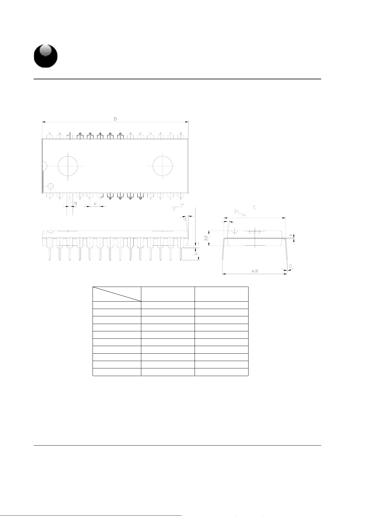
PACKAGE OUTLINE DIMENSION
28 pin ( 600mil ) PDIP Package Outline Dimension
UT6264C
8K X 8 BIT LOW POWER CMOS SRAM
SYMBOL
UNIT
A1 0.010 (MIN) 0.254 (MIN)
A2 0.150
B 0.018
c 0.010
D 1.460
E 0.600
e 0.100 (TYP) 2.540 (TYP)
eB 0.640±0.03 16.256
L 0.130
Θ
0
INCH(BASE) MM(REF)
±
0.01 3.810
±
0.005 0.457
±
0.004 0.254
±
0.005 37.084
±
0.010 15.240
±
0.010 3.302
o
o
∼
15
0
o
∼
±
±
±
±
±
±
±
15
0.254
0.127
0.102
0.127
0.254
0.762
0.254
o
UTRON TECHNOLOGY INC. P80028
1F, No. 11, R&D Rd. II, Science-Based Industrial Park, Hsinchu, Taiwan, R. O. C.
TEL: 886-3-5777882 FAX: 886-3-5777919
8
Page 10
UTRON
Rev. 1.4
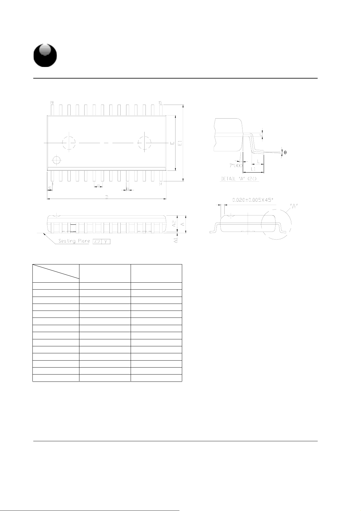
28 pin 330 mil SOP Package Outline Dimension
UT6264C
8K X 8 BIT LOW POWER CMOS SRAM
SYMBOL
UNIT
A 0.112(max) 2.845(max)
A1 0.004(MIN) 0.102(MIN)
A2 0.098±0.005 2.489±0.127
b 0.016(TYP) 0.406(TYP)
c 0.010(TYP) 0.254(TYP)
D 0.713±0.005 18.110±0.127
E 0.331±0.005 8.407±0.127
E1 0.465±0.012 11.811±0.305
e 0.050(TYP) 1.270(TYP)
L 0.0404±0.008 1.0255±0.203
L1 0.067±0.008 1.702±0.203
S 0.047(MAX) 1.194(MAX)
y 0.003(MAX) 0.076(MAX)
θ 0°~10° 0°~10°
INCH(BASE) MM(REF)
UTRON TECHNOLOGY INC. P80028
1F, No. 11, R&D Rd. II, Science-Based Industrial Park, Hsinchu, Taiwan, R. O. C.
TEL: 886-3-5777882 FAX: 886-3-5777919
9
Page 11
Rev. 1.4
UTRON
8K X 8 BIT LOW POWER CMOS SRAM
UT6264C
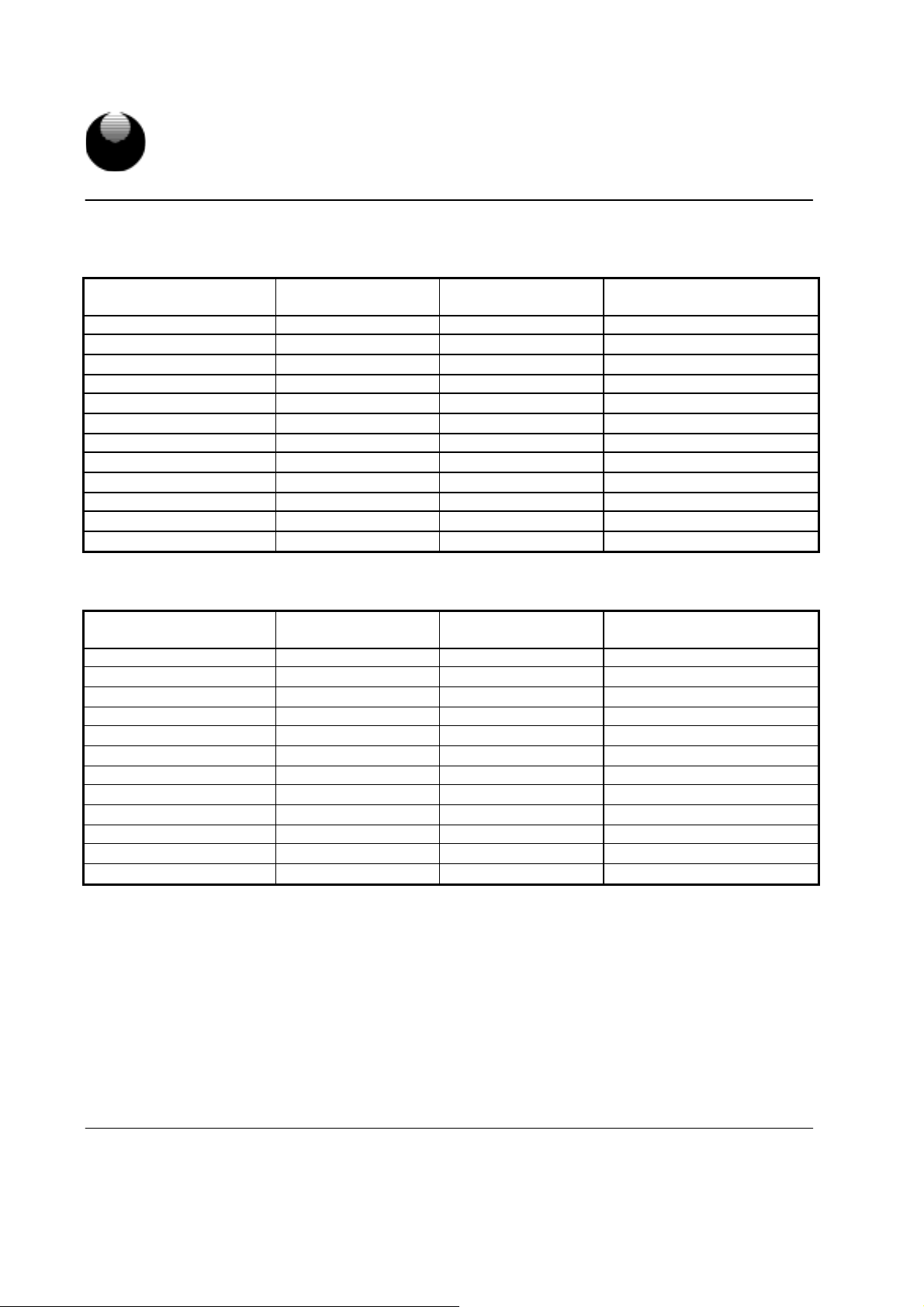
ORDERING INFORMATION
Commerical temperature
PART NO.
UT6264CPC-35 35 0.3mA 28 PIN PDIP
UT6264CPC-35L 35 2µA 28 PIN PDIP
UT6264CPC-35LL 35 1µA 28 PIN PDIP
UT6264CPC-70 70 0.3mA 28 PIN PDIP
UT6264CPC-70L 70 2µA 28 PIN PDIP
UT6264CPC-70LL 70 1µA 28 PIN PDIP
UT6264CSC-35 35 0.3mA 28 PIN SOP
UT6264CSC-35L 35 2µA 28 PIN SOP
UT6264CSC-35LL 35 1µA 28 PIN SOP
UT6264CSC-70 70 0.3mA 28 PIN SOP
UT6264CSC-70L 70 2µA 28 PIN SOP
UT6264CSC-70LL 70 1µA 28 PIN SOP
Extended temperature
PART NO.
UT6264CPC-35E 35 0.3mA 28 PIN PDIP
UT6264CPC-35LE 35 2µA 28 PIN PDIP
UT6264CPC-35LLE 35 1µA 28 PIN PDIP
UT6264CPC-70E 70 0.3mA 28 PIN PDIP
UT6264CPC-70LE 70 2µA 28 PIN PDIP
UT6264CPC-70LLE 70 1µA 28 PIN PDIP
UT6264CSC-35E 35 0.3mA 28 PIN SOP
UT6264CSC-35LE 35 2µA 28 PIN SOP
UT6264CSC-35LLE 35 1µA 28 PIN SOP
UT6264CSC-70E 70 0.3mA 28 PIN SOP
UT6264CSC-70LE 70 2µA 28 PIN SOP
UT6264CSC-70LLE 70 1µA 28 PIN SOP
ACCESS TIME
(ns)
ACCESS TIME
(ns)
STANDBY CURRENT
(µA) (TYP.)
STANDBY CURRENT
(µA) (TYP.)
PACKAGE
PACKAGE
UTRON TECHNOLOGY INC. P80028
1F, No. 11, R&D Rd. II, Science-Based Industrial Park, Hsinchu, Taiwan, R. O. C.
TEL: 886-3-5777882 FAX: 886-3-5777919
10
Page 12
Rev. 1.4
UTRON
8K X 8 BIT LOW POWER CMOS SRAM
UT6264C
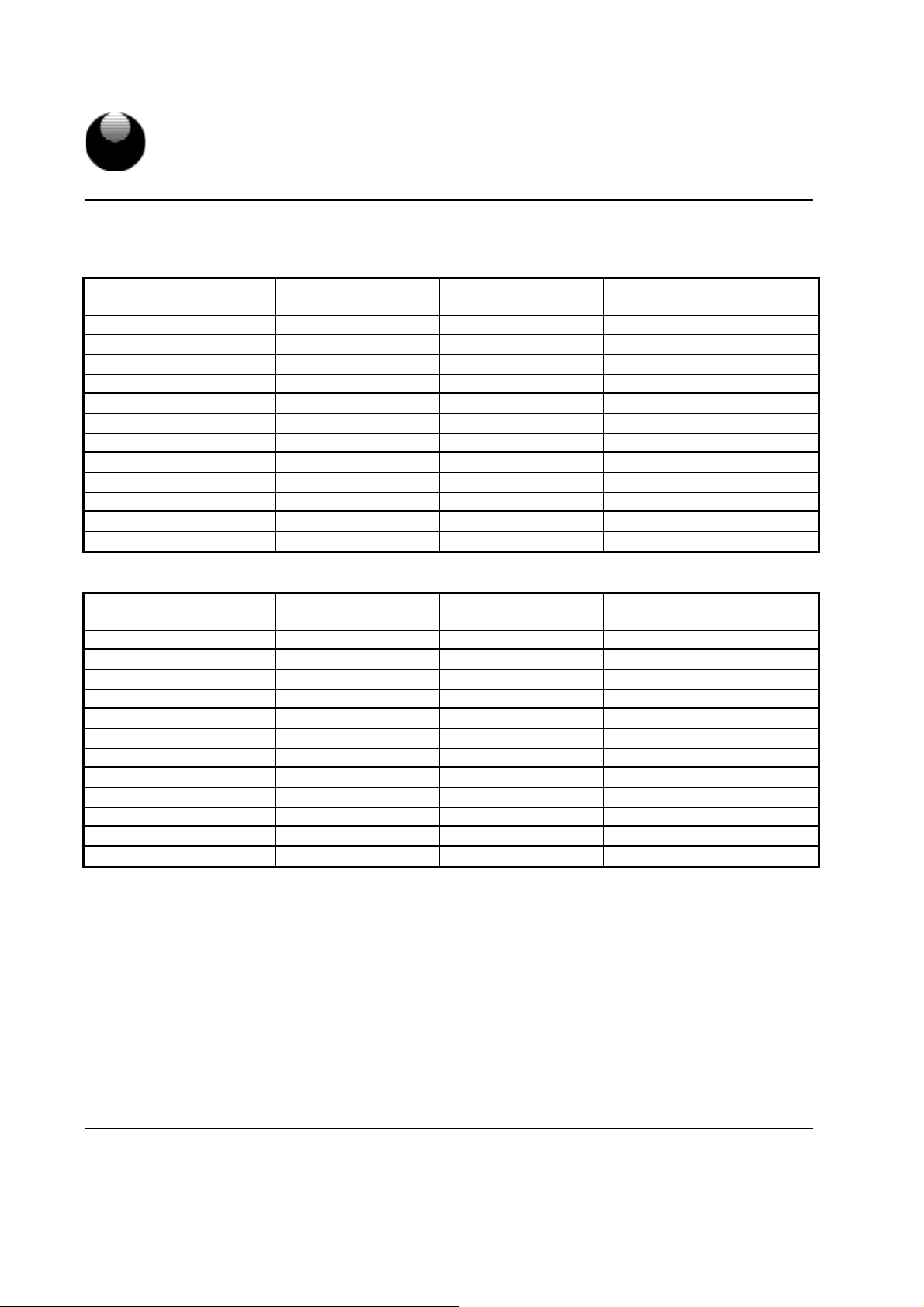
ORDERING INFORMATION (for lead free product)
Commerical temperature
PART NO.
UT6264CPCL-35 35 0.3mA 28 PIN PDIP
UT6264CPCL-35L 35 2µA 28 PIN PDIP
UT6264CPCL-35LL 35 1µA 28 PIN PDIP
UT6264CPCL-70 70 0.3mA 28 PIN PDIP
UT6264CPCL-70L 70 2µA 28 PIN PDIP
UT6264CPCL-70LL 70 1µA 28 PIN PDIP
UT6264CSCL-35 35 0.3mA 28 PIN SOP
UT6264CSCL-35L 35 2µA 28 PIN SOP
UT6264CSCL-35LL 35 1µA 28 PIN SOP
UT6264CSCL-70 70 0.3mA 28 PIN SOP
UT6264CSCL-70L 70 2µA 28 PIN SOP
UT6264CSCL-70LL 70 1µA 28 PIN SOP
ACCESS TIME
(ns)
STANDBY CURRENT
(µA) (TYP.)
PACKAGE
Extended temperature
PART NO.
UT6264CPCL-35E 35 0.3mA 28 PIN PDIP
UT6264CPCL-35LE 35 2µA 28 PIN PDIP
UT6264CPCL-35LLE 35 1µA 28 PIN PDIP
UT6264CPCL-70E 70 0.3mA 28 PIN PDIP
UT6264CPCL-70LE 70 2µA 28 PIN PDIP
UT6264CPCL-70LLE 70 1µA 28 PIN PDIP
UT6264CSCL-35E 35 0.3mA 28 PIN SOP
UT6264CSCL-35LE 35 2µA 28 PIN SOP
UT6264CSCL-35LLE 35 1µA 28 PIN SOP
UT6264CSCL-70E 70 0.3mA 28 PIN SOP
UT6264CSCL-70LE 70 2µA 28 PIN SOP
UT6264CSCL-70LLE 70 1µA 28 PIN SOP
UTRON TECHNOLOGY INC. P80028
1F, No. 11, R&D Rd. II, Science-Based Industrial Park, Hsinchu, Taiwan, R. O. C.
TEL: 886-3-5777882 FAX: 886-3-5777919
ACCESS TIME
(ns)
STANDBY CURRENT
(µA) (TYP.)
11
PACKAGE
Page 13

Rev. 1.4
UTRON
THIS PAGE IS LEFT BLANK INTENTIONALLY.
UT6264C
8K X 8 BIT LOW POWER CMOS SRAM
UTRON TECHNOLOGY INC. P80028
1F, No. 11, R&D Rd. II, Science-Based Industrial Park, Hsinchu, Taiwan, R. O. C.
TEL: 886-3-5777882 FAX: 886-3-5777919
12
 Loading...