

UTMC 5962R9858003VXC, 5962R9858003QXC, 5962R9858002VXC, 5962R9858001VXC, 5962R9858001QXC Datasheet
1
UT54ACS164245S
RadHard Schmitt CMOS 16-bit Bidirectional MultiPurpose Transceiver
Datasheet
April , 2002
FEATURES
• Voltage translation
- 5V bus to 3.3V bus
- 3.3V bus to 5V bus
• Cold sparing
- 1M Ω minimum input impedance power-off
• 0.6µm Commercial RadHardTM CMOS
- Total dose: 100K rad(Si)
- Single Event Latchup immune
• High speed, low power consumption
• Schmitt trigger inputs to filter noisy signals
• Available QML Q or V processes
• Standard Microcircuit Drawing 5962-98580
• Package:
- 48-lead flatpack, 25 mil pitch (.390 x .640)
DESCRIPTION
The 16-bit wide UT54ACS164245S MultiPurpose transceiver
is built using UTMC’s Commercial RadHard
TM
epitaxial
CMOS technology and is ideal for space applications. This high
speed, low power UT54ACS164245S transceiver is designed to
perform multiple functions including: asynchronous two-way
communication, signal buffering, voltage translation, and cold
sparing. With V
DD
equal to zero volts, the UT54ACS164245S
outputs and inputs present a minimum impedance of 1MΩ making it ideal for "cold spare" applications. Balanced outputs and
low "on" output impedance make the UT54ACS164245S well
suited for driving high capacitance loads and low impedance
backplanes. The UT54ACS164245S enables system designers
to interface 3.3 volt CMOS compatible components with 5 volt
CMOS components. For voltage translation, the A port interfaces with the 3.3 volt bus; the B port interfaces with the 5 volt
bus. The direction control (DIRx) controls the direction of data
flow. The output enable (OEx) overrides the direction control
and disables both ports. These signals can be driven from either
port A or B. The direction and output enable controls operate
these devices as either two independent 8-bit transceivers or one
16-bit transceiver.
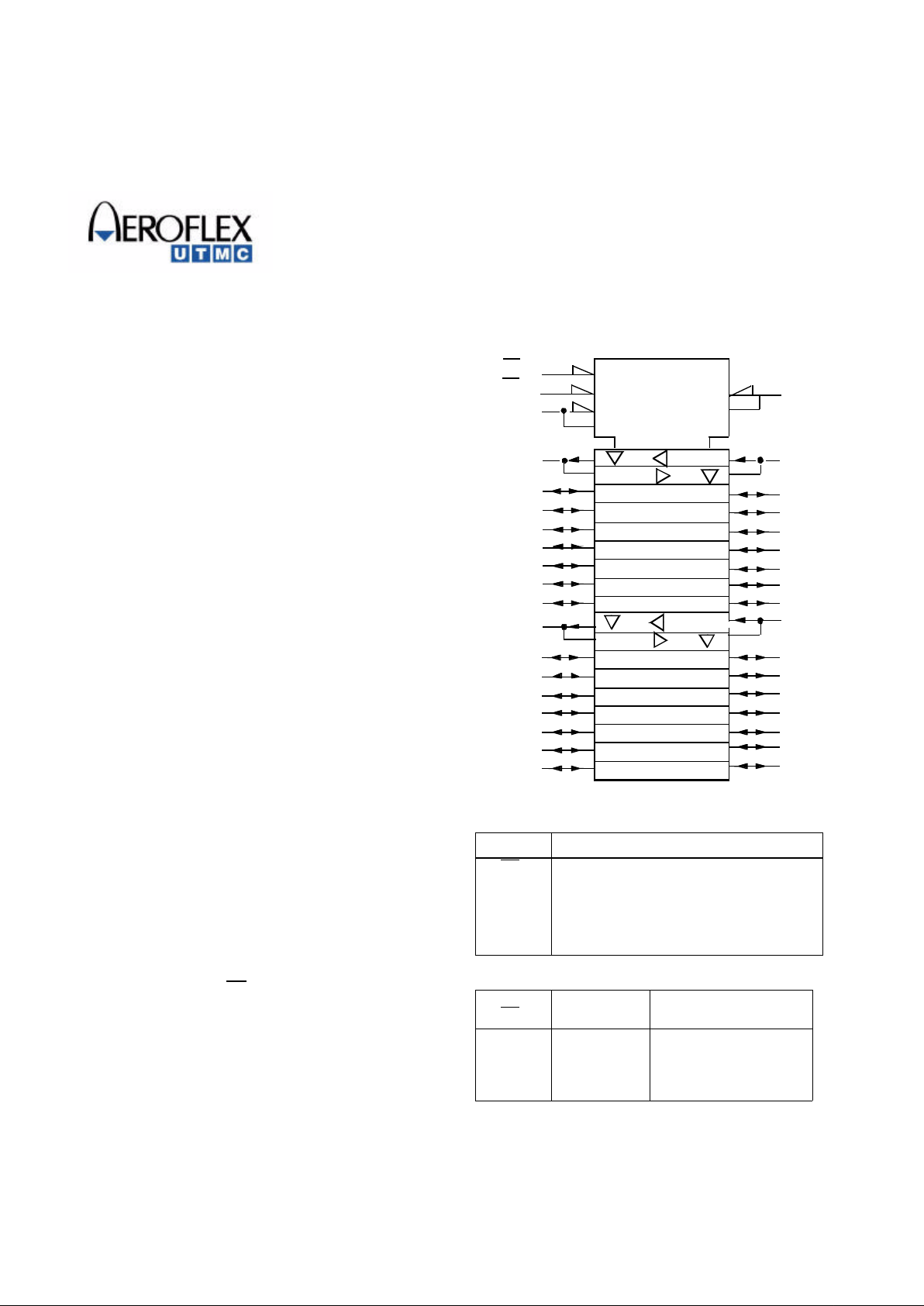
LOGIC SYMBOL
PIN DESCRIPTION
FUNCTION TABLE
Pin Names Description
OE x Output Enable Input (Active Low)
DIRx Direction Control Inputs
xAx Side A Inputs or 3-State Outputs (3.3V Port)
xBx Side B Inputs or 3-State Outputs (5V Port)
ENABLE
OE x
DIRECTION
DIRx OPERATION
L L B Data To A Bus
L H A Data To B Bus
H X Isolation
(48)OE1
G2
(47)
1A1
(46)
1A2
(44)
(2)
1B1
(5)
(3)
1B2
1A3
(43)
1A4
(41)
1A5
(40)
1A6
1B3
(9)
1B6
(8)
1B5
(6)
1B4
(38)
1A7
(37)
1A8
(12)
1B8
(11)
1B7
(1)
DIR1 1EN1 (BA)
1EN2 (AB)
11
12
(25)OE2
G1
(24)
DIR2
21
22
(36)
2A1
2B1
(13)
(35)
2A2
(33)
2A3
(32)
2A4
(30)
2A5
(29)
2A6
(27)
2A7
(26)
2A8
(16)
2B2
2B3
(20)
2B6
(19)
2B5
(17)
2B4
(23)
2B8
(22)
2B7
(14)
2EN1 (BA)
2EN2 (AB)
2
PINOUTS
POWER TABLE
1
NOTE:
1. V
DD2
cannot be tied to VSS while power is applied to V
DD1
.
Control signals DIRx and OEx are 5 volt tolerant inputs. When
V
DD2
is at 3.3 volts, either 3.3 or 5 volt CMOS logic levels can
be applied to all control inputs. For proper operation connect
power to all VDD and ground all VSS pins (i.e., no floating VDD
or VSS input pins). Tie unused inputs to VSS. If V
DD1
and
V
DD2
are not powered up together, then V
DD2
should be pow-
ered up first for proper control of OE and DIR. Until V
DD2
reaches 2.75V + 5%, control of the outputs by OE and DIR cannot be guaranteed. During operation of the part, after power up,
insure V
DD1
> V
DD2
. Tie unused inputs to VSS.
1
2
3
4
5
7
6
48
47
46
45
44
42
43
DIR1
1B1
1B2
V
SS
1B3
1B4
VDD1
OE1
1A1
1A2
V
SS
1A3
VDD2
8 41
1B5
1A5
1A4
9 40
1B6
1A6
10 39
V
SS
V
SS
48-Lead Flatpack
Top View
1B7
1B8
2B1
2B2
V
SS
2B3
2B4
VDD1
2B5
2B6
11
12
13
14
15
17
16
18
19
20
V
SS
2B7
2B8
DIR2
21
22
23
24
38
37
36
35
34
32
33
1A7
1A8
2A1
2A2
V
SS
2A4
31 VDD2
2A3
30 2A5
29 2A6
28 V
SS
27
2A7
26 2A8
25 OE2
Port B Port A OPERATION
5 Volts 3.3 Volts Voltage Translator
5 Volts 5 Volts Non Translating
3.3 Volts 3.3 Volts Non Translating
V
SS
V
SS
Cold Spare
V
SS
3.3V or 5V Port B Cold Spare
3
LOGIC DIAGRAM
1A1
1A2
1A3
1A4
1A5
1A6
1A7
1A8
DIR1
(1)
(47)
(48)
(2)
(46)
(3)
(44)
(5)
(43)
(6)
(41)
(8)
(40)
(9)
(38)
(11)
(37)
(12)
1B1
1B2
1B3
1B6
1B5
1B4
1B8
1B7
OE1
2A1
2A2
2A3
2A4
2A5
2A6
2A7
2A8
DIR2
(24)
(36)
(25)
(13)
(35)
(14)
(33)
(16)
(32)
(17)
(30)
(19)
(29)
(20)
(27)
(22)
(26)
(23)
2B1
2B2
2B3
2B6
2B5
2B4
2B8
2B7
OE 2
3.3V PORT
5 V PORT
3.3V PORT
5 V PORT
4
RADIATION HARDNESS SPECIFICATIONS
1
Notes:
1. Logic will not latchup during radiation exposure within the limits defined in the table.
2. Not tested, inherent of CMOS technology.
ABSOLUTE MAXIMUM RATINGS
1
Note:
1. Stresses outside the listed absolute maximum ratings may cause permanent damage to the device. This is a stress rating only, functional operation of the device
at these or any other conditions beyond limits indicated in the operational sections is not recommended. Exposure to absolute maximum rating conditions for
extended periods may affect device reliability and performance.
DUAL SUPPLY OPERATING CONDITIONS
PARAMETER LIMIT UNITS
Total Dose 1.0E5 rad(Si)
SEL Latchup >120
MeV-cm2/mg
Neutron Fluence
2
1.0E14
n/cm
2
SYMBOL PARAMETER LIMIT (Mil only) UNITS
V
I/O
Voltage any pin -.3 to V
DD1
+.3 V
V
DD1
Supply voltage -0.3 to 6.0 V
V
DD2
Supply voltage -0.3 to 6.0 V
T
STG
Storage Temperature range -65 to +150 °C
T
J
Maximum junction temperature +175 °C
Θ
JC
Thermal resistance junction to case 20 °C/W
I
I
DC input current ±10 mA
P
D
Maximum power dissipation 1 W
SYMBOL PARAMETER LIMIT UNITS
V
DD1
Supply voltage 3.0 to 3.6 or 4.5 to 5.5 V
V
DD2
Supply voltage 3.0 to 3.6 or 4.5 to 5.5 V
V
IN
Input voltage any pin 0 to V
DD1
V
T
C
Temperature range -55 to + 125 °C

5
DC ELECTRICAL CHARACTERISTICS
1
( -55°C < TC < +125°C) (TC = -55°°C to +125°°C for "C" screening and -40 °°C to +125 °°C for "W" screening)
SYMBOL PARAMETER CONDITION MIN MAX UNIT
VT+
Schmitt Trigger, positive going threshold
2
VDD from 3.00 to 5.5 .7V
DD
V
VT-
Schmitt Trigger, negative going threshold
2
VDD from 3.00 to 5.5 .3V
DD
V
V
H1 Schmitt Trigger range of hysteresis
10
VDD from 4.5 to 5.5
0.6 V
V
H2 Schmitt Trigger range of hysteresis
10
VDD from 3.00 to 3.6 0.4 V
I
IN Input leakage current
10
VDD from 3.6 to 5.5
VIN = VDD or V
SS
-1 3 µA
I
OZ Three-state output leakage current
10
VDD from 3.6 to 5.5
VIN = VDD or V
SS
-1 3 µA
I
CS Cold sparing leakage current
3
VIN = 5.5
VDD = V
SS
-1 5 µA
I
OS1 Short-circuit output current
6, 11
VO = V
DD
or V
SS
VDD from 4.5 to 5.5
-200 200 mA
I
OS2 Short-circuit output current
6, 11
VO = V
DD
or V
SS
VDD from 3.00 to 3.6
-100 100 mA
V
OL1
Low-level output voltage
4, 10
IOL= 8mA
IOL= 100µA
VDD = 4.5
0.4
0.2
V
V
OL2
Low-level output voltage
4, 10
IOL= 8mA
IOL= 100µA
VDD = 3.00
0.5
0.2
V
V
OH1 High-level output voltage
4, 10
IOH= -8mA
IOH= -100 µA
VDD = 4.5
V
DD
- 0.7
VDD - 0.2
V
V
OH2 High-level output voltage
4, 10
IOH= -8mA
IOH= -100 µA
VDD = 3.00
V
DD
- 0.9
VDD - 0.2
V
 Loading...