

UTMC 5962R9855202VZC, 5962R9855202VYC, 5962R9855202VXX, 5962R9855202VXC, 5962R9855202VXA Datasheet
...
Standard Products
UT69R000 RadHard MicroController
Data Sheet
July 2002
q Harvard architecture
- 64K data space
- 1M instruction space
q High throughput engine
- 2 clocks per instruction
- 8 MIPS @ 16 MHz
- Static design
q 15 levels of interrupts
- 8 external user defined interrupts
- Machine error and power fail
q Two on-board 16-bit interval timers
- Timer A, 10 µs/bit
- Timer B, 100 µs/bit resolution
q 8-bit software controlled output discrete bus
q Register- oriented architecture has 21
user-accessible registers
- 16-bit or 32-bit register configurations
q Supports direct memory access (DMA) system
configuration
q Built-in 9600 baud UART
q Full military operating temperature range, -55oC to
+125oC, in accordance with MIL-PRF-38535 for Class Q
or V
q Typical radiation performance:
- Total dose: 1.0E6 rads(Si)
- SEL Immune >100 MeV-cm2/mg
- LETTH(0.25) = 60 MeV-cm2/mg
- Saturated Cross Section (cm2) per bit, 1.2E-7
- 2.3E-11 errors/bit-day, Adams to 90%
geosynchronous heavy ion
q Post-radiation AC/DC performance characteristics
guaranteed by MIL-STD-883 Method 1019 testing
at 1.0E6 rads(Si)
q Latchup immune 1.5-micron CMOS, epitaxial,
double-level-metal technology
q Packaging options:
- 132-lead flatpack
- 144-pin pingrid array (plus one index pin)
32
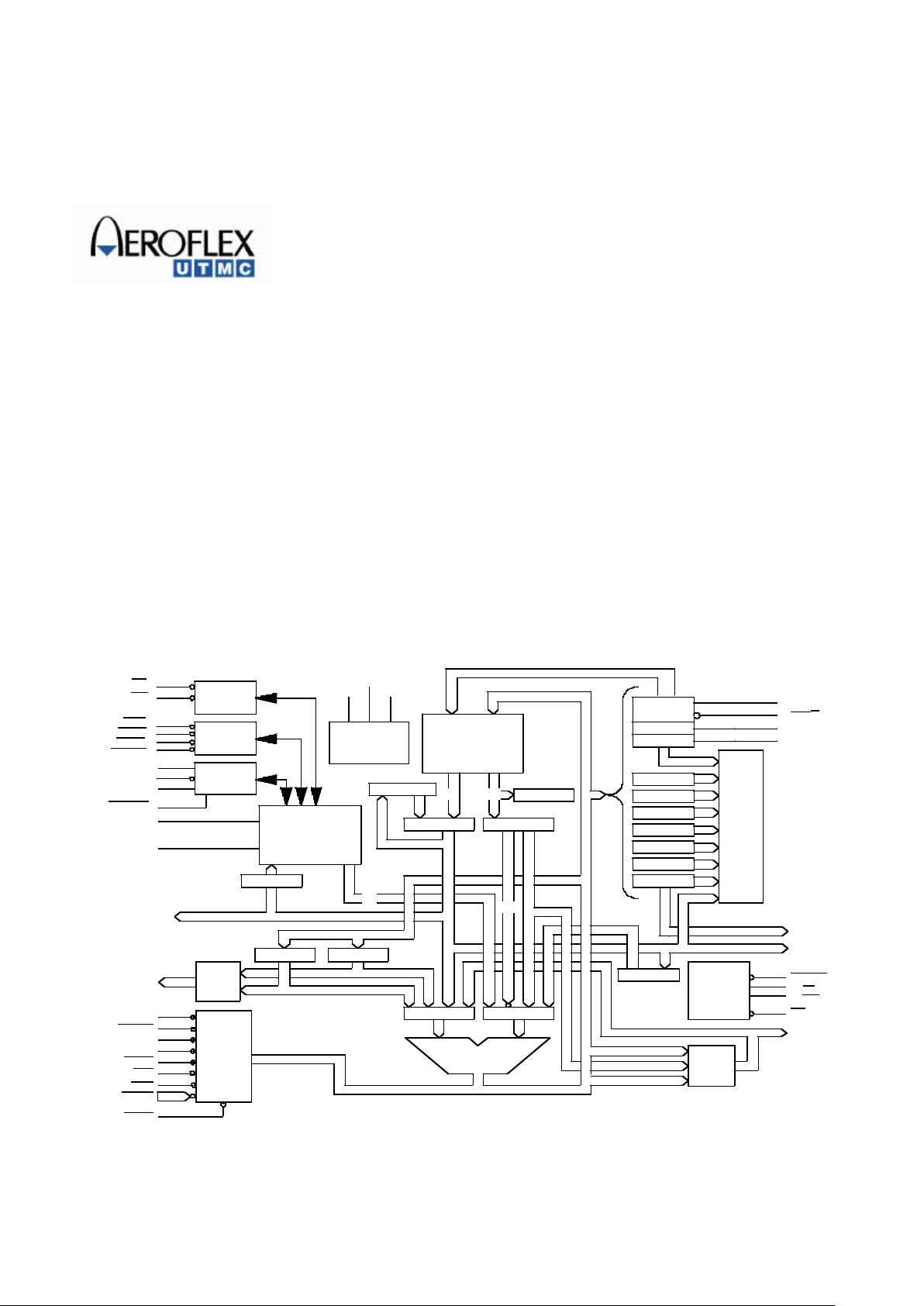
Figure 1. UT69R000 Functional Block Diagram
OE
WE
BRQ
BGNT
BUSY
BGACK
NUI1
NUI2
NUI3
STATE1
DI1
DI2
INSTRUCTION
DATA
INSTRUCTION
ADDRESS
MCHNE1
BTERR
MCHNE2
MPROT
PFAIL
INT5
INT6
INT0-4
MRST
20
16
32
32
32
ADD
MUX
MEMORY
CONTROL
BUS
ARBITRA-
TION
PROCES-
SOR
STATUS
PROCESSOR
CONTROL
LOGIC
OSCILLATOR
/CLOCK
GENERAL
PURPOSE
REGISTERS
OSCIN
OSCOUT
SYSCLK
ID
IC/ICs ACC
SHIFT REG
TEMP DEST
32
32
TEMP SRC
BIT REG
32
32
A MUX B MUX
32-BIT ALU
16
32
16
16
ADDR
MUX
BUS
CONTROL
UART
TBR
RBR
TIMCLK
TEST
UARTOUT
UARTIN
TR
TB
IM
FR
PI
ST
SW
16
16
16
16
5
16
8
OD(7:0)
OPERAND
DATA
DTACK
M/IO
R/ WR
DS
OPERAND
ADDRESS
PIPELINE
I/O
MUX
INTERRUPTS
16
16
16
16

2
Table of Contents
1.0 Introduction.....................................................................................................................4
1.1 General Description ..............................................................................................4
1.2 General Operation.................................................................................................4
2.0 Register File .................................................................................................................... 6
2.1 General Purpose Registers ....................................................................................6
2.2 Specialized Registers ............................................................................................6
2.2.1 Specialized Register Description.................................................................6
3.0 Instruction Port..............................................................................................................16
3.1 Instruction Port Operations.................................................................................17
3.1.1 STRI Instruction Bus Cycle .......................................................................17
3.1.2 LRI Instruction Bus Cycle.........................................................................18
4.0 Operand Port ................................................................................................................. 19
4.1 Operand Bus Cycle Operation ............................................................................20
4.2 DMA Operation and Bus Arbitration..................................................................23
5.0 Discrete Input/Output....................................................................................................25
5.1 Output Discrete Bus............................................................................................25
5.2 Discrete Inputs .................................................................................................... 26
6.0 Interrupts ....................................................................................................................... 26
6.1 Interrupt Control .................................................................................................26
6.1.1 Interrupt Status........................................................................................... 27
6.1.2 Interrupt Processing and Vectoring ...........................................................27
6.2 Interrupt Sources.................................................................................................28
6.3 Interrupt Hardware..............................................................................................28
6.4 Interrupt Latency.................................................................................................28
7.0 Monitor .........................................................................................................................28
7.1 Using the Monitor...............................................................................................29
7.1.1 Examine Command.................................................................................... 33
7.1.2 Modify Command ...................................................................................... 33
7.1.3 Continue Command...................................................................................34
7.1.4 Run Command...........................................................................................34
8.0 Internal UART Operation .............................................................................................34
8.1 UART Transmitter Operation.............................................................................34
8.2 UART Receiver Operation..................................................................................35
9.0 Programming Interface..................................................................................................35
9.1 Data Formats.......................................................................................................35
9.2 Instruction Formats .............................................................................................36
9.3 Addressing Modes...............................................................................................37
9.4 Data Movement Operations ................................................................................38
10.0 Pin Description..............................................................................................................39
11.0 Absolute Maximum....................................................................................................... 46
12.0 Recommended Operating Conditions ........................................................................... 46
13.0 DC Electrical Characteristics ........................................................................................47
14.0 AC Electrical Characteristics ........................................................................................48
15.0 Packaging ...................................................................................................................... 58
16.0 Ordering ........................................................................................................................60
3
DS
R/
M/
DTACK
BGACK
BUSY
BGNT
BRQ
MCHNE1
WE
OE
MRST
INT6
INT5
PFAIL
INT0
INT1
INT2
INT3
INT4
NUI4
TEST
EXCEPTIONS
INTERRUPTS/
INSTRUCTION DATA PORT
OSCIN
OSCOUT
UARTIN
UARTOUT
TIMCLK
UT69R000
RA19
RA18
RA17
RA16
RA15
RA14
RA13
RA12
RA11
RA10
RA9
RA8
RA7
RA6
RA5
RA4
RA3
RA2
RA1
RA0
NUI1
NUI3
BTERR
MCHNE2
MPROT
A0
A1
A2
A3
A4
A5
A6
A7
A8
A9
A10
A11
A12
A13
A14
A15
OD7
OD6
OD5
OD4
OD3
OD2
OD1
SYSCLK
INSTRUCTION
ADDRESS
BUS
PROCESSOR
STATUS
OSCILLATOR
UART
DATA BUS
MEMORY
ADDRESS
BUS
CLOCK
OUTPUT
BUS
CONTROL
BUS
ARBITRATION
OD0
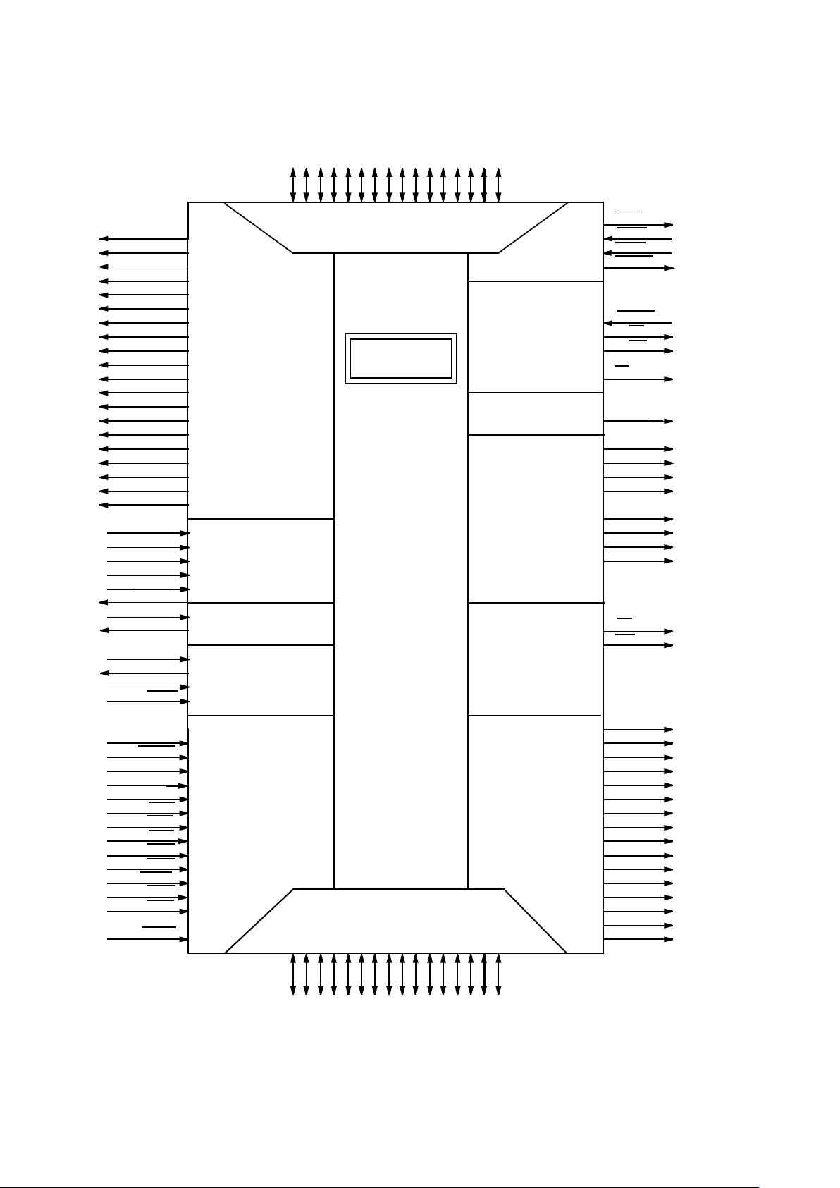
Figure 2. UT69R000 Pin Function Diagram
DI1
DI2
STATE1
RD0 - RD15
D0 - D15
OPERAND
OPERAND
NUI2
DISCRETES
WR
IO
4
1.0 Introduction
The UT69R000 is a radiation-hardened high-performance
microcontroller designed, manufactured, and tested to meet
rigorous radiation environments. UTMC designed and
implemented the UT69R000 using an advanced radiationhardened twin-well CMOS process. The combination of
radiation-hardness, high throughput, and low power
consumption makes the UT69R000 ideal for high-speed
systems in satellites, missiles, and avionics applications.
1.1 General Description
The UT69R000 is a versatile microcontroller designed to meet
real-time control type applications. Support functions often
found external to a microprocessor are integrated within the
microcontroller. Functions include UART, interval timers, 10
external interrupt vectors, and a 8-bit output discrete bus.
The UT69R000 core (machine) is a two port microcontroller
that accesses instructions from a 1M x 16 instruction port; a
second port (64K x 16 data port) is available for data storage.
Data transfer acknowledge allows the addition of wait states
on the data port. The machine performs overlapping fetches
and executes speeding instruction throughput. A 12 MHz
operating clock frequency provides up to 6 MIPS of
throughput. A later section of this data sheet expands on this
concept.
The UT69R000 architecture is based on 20 16-bit general
purpose registers providing, the programmer with extensive
register support. The UT69R000’s flexibility is enhanced by
the concatenation of 16-bit registers into 32-bit registers. In
addition, all registers are available for use as either the source
or destination for any register operation.
All UT69R000 circuitry is of static design. Internal registers,
counters, and latches do not require refresh as with dynamic
circuit design. Therefore the UT69R000 can operate from DC
to the upper frequency limit of 16 MHz. This type of operation
is especially useful in power critical applications such as
satellites.
The UT69R000 fully supports multiprocessor systems, DMA,
and complex bus arbitration. Bus control passes among bus
masters operating on the same bus. The bus master can be one
of several UT69R000s or any other device requiring DMA.
The UT69R000 supports 15 levels of vectored interrupts. Ten
of these are external interrupts, all of which are user-definable.
All interrupts are serviced in order of priority.
The UT69R000’s three basic instruction formats support 16bit and 32-bit instruction. The formats are Register-to-Register,
Register-to-Literal, and Register-to-Long-Immediate
instructions.
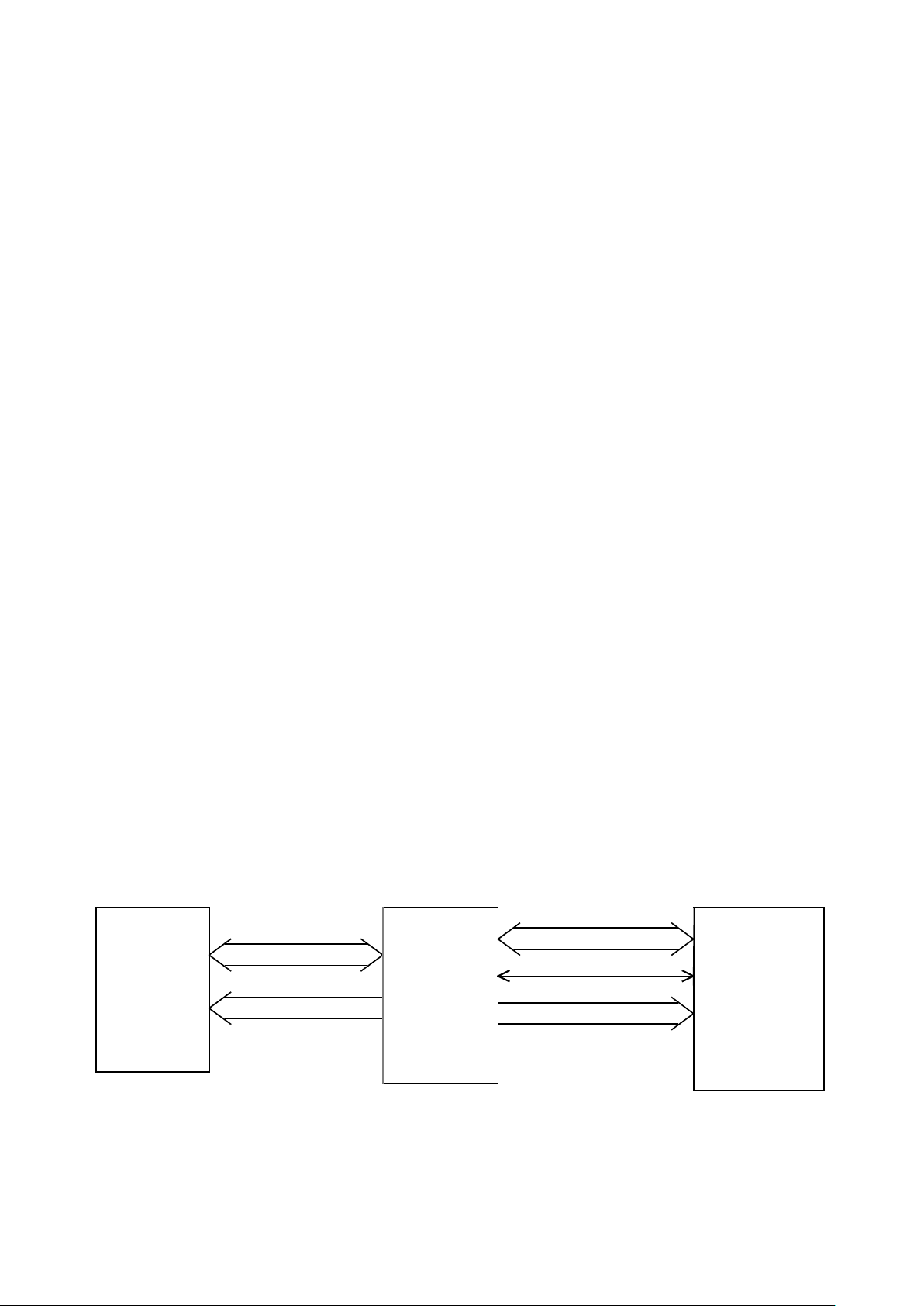
Figure 3 shows the UT69R000’s general system architecture.
1.2 General Operation
The UT69R000 reduced instruction set consists of 35 separate
instructions. Most of these instructions execute in two clock
cycles providing high-throughput. The UT69R000 has a
Harvard architecture which incorporates two address and two
data buses. One set of address and data buses interface with
instruction memory (instruction port) and the other interfaces
with data memory (data port). The instruction port consists of
a 20-bit address bus and 16-bit data bus. The maximum
program length of any program is 1 mega-word. The data port
consists of a 16-bit address and data bus, allowing access to
64K x 16 of data storage.
The instruction port is dedicated to the storage of instruction
code; however , two instructions exist that allow the instruction
port manipulation by the machine. These instructions are the
Load Register from Instruction Memory (LRI) and Store
Register to Instruction Memory (STRI).
16
20
16
16
ADDRESS
Figure 3. UT69R000 General System Architecture
CONTROL
DATA
MEMORY
INSTRUCTION
INSTRUCTION
INSTRUCTION
UT69R000
DATA
MEMORY
DATA
ADDRESS
5
The UT69R000 begins operation by first generating an address
on the instruction port; valid data (instruction) is then latched
into the Primary Instruction Register (PIR). After the machine
stores the instruction in the PIR, the machine begins execution
of the instruction in the Instruction Register (IR). If the present
instruction in the IR requires only internal processing, the
machine does not exercise the data bus. If the machine needs
additional data to complete the instruction the machine begins
arbitration for the data port.
Data port arbitration begins with the machine asserting the Bus
Request (BRQ) signal. The machine samples the Bus Grant
(BGNT) and Bus Busy (BUSY) signals on the falling edge of
the clock (OSCIN). When the machine detects that the previous
bus controller has relinquished control of the bus, the machine
generates a Bus Grant Acknowledge (BGACK) signal
signifying that it has taken control of the bus (i.e., data port).
After the UT69R000 takes control of the bus, it generates valid
address and data information. If the machine is interfacing to
slow memory or other peripheral devices that require long
memory-access times, the Data Transfer Acknowledge
(DTACK) signal extends the memory cycle time. By holding
off the assertion of DTACK, the slow device lengthens the
memory cycle until it can provide data for the machine.
The UT69R000 controls the vectoring and prioritizing of
interrupt service. Internal logic selects one of 15 interrupt
vectors, each interrupt vector is allocated four memory
locations. Use the four memory locations to store return from
interrupt service address information along with the interrupt
service routine’s location. The UT69R000 controls prioritizing
of coincident interrupts.
Perform UART control and maintenance via input/output
commands OTR and INR. These commands allow the
programmer to read UART status, and error information, as
well as upload and download information to the receive and
transmit buffers respectively.
Figure 4 shows an example of a system configuration.
INSTRUCTION
DATA
INSTRUCTION
ADD
16
20
NUI3
USERDEFINED
SYSTEM
INTERRUPTS
8
UART
I/F
X
C
V
R
GENERAL
PURPOSE
MEMORY
I/O
DEVICE #1
I/O
DEVICE #2
BUS
ARBITER
DMA
DEVICE
#1
1553
I/F
DMA
DEVICE
#2
OP ADD
OP DATA
CONTROL
16
16
6
Figure 4. The UT69R000 Example System Configuration
4
UT69R000
INSTRUCTION MEMORY
CAN ONLY BE ACCESSED
BY THE UT69R000
INSTRUCTION
MEMORY
1M X 16
INTERNALLY
PULLED LOW
SERIAL I/O
BUSY
BGACK
BRQ
BGNT
OE
WE
(MAX)
6
2.0 Register File
The UT69R000 has a register-oriented architecture. The
registers within the machine fall into two categories, general
purpose and specialized registers. All registers are accessible
to the programmer through the instruction set. The programmer
uses data from these registers to perform arithmetic and logical
functions, alter program flow, detect various system and
machine faults, determine machine status, control UART and
timer functions, and for exception handling.
2.1 General Purpose Registers
Figure 5 shows the UT69R000’s 20 general purpose registers.
The UT69R000 normally accesses these registers as singleword 16-bit registers although the machine can concatenate
these registers into 32-bit double-word register pairs. When the
programmer uses the general purpose registers as a doubleword register pair, the most significant 16 bits of the 32-bit
words are stored in the even-numbered register of the register
pair. For instance, if a 32-bit word is stored in Register Pair
XR6, the most significant word is stored in register R6 and the
least significant word is stored in register R7.
In addition to the 20 general purpose registers, the UT69R000
has a 32-bit accumulator (ACC). The ACC is normally a
destination register, although under certain circumstances it
can be the source register (INR RD, ACC). The accumulator
retains the most significant half of the product during a multiply
instruction or the remainder during a divide operation.
2.2 Specialized Registers
The UT69R000 has 13 special purpose registers. These
registers control machine configuration, report status, and
interrupts. Below is a list of the special purpose registers. The
values in the brackets indicate the power-up condition.
1. Stack Pointer Register (SP) [XXXX (hex)]
2. System Status Register (STATUS) [XXXX (hex)]
3. UART Receiver Buffer Register (RCVR)
[XX00 (hex)]
4. UART Transmitter Buffer Register (TXMT)
[XX00 (hex)]
5. Pending Interrupt Register (PI) [0000 (hex)]
6. Fault Register (FT) [0000 (hex)]
7. Interrupt Mask Register (MK) [XXXX (hex)]
8. Status/Output Discrete Register (SW)
[XXFF (hex)]
9. Instruction Counter Register (IC) [0000 (hex)]
10. Instruction Counter Save Register (ICS)
[XXXXX (hex)]
11. Instruction Register (IR) [0000 (hex)]
12. Timer A (TA) [0000 (hex)]
13. Timer B (TB) [0000 (hex)]
The instruction set provides access to most of the special
purpose registers.
2.2.1 Register Description
Stack Pointer Register
The UT69R000 uses the 16-bit Stack Pointer Register as an
address pointer on PUSH and POP instructions. The machine
pre-increments (POP) and post-decrements (PUSH) the Stack
Pointer contents. The programmer loads and stores the SP by
executing the INR and OTR commands to the stack pointer.
Bit 15 is the most significant bit, the least significant bit is bit
zero.
System Status Register
The System Status Register provides status information on the
UT69R000’s internal operation, including status of the internal
UART. The register is read via the INR Rd, STATUS
instruction. Bit definitions follow.
Figure 5. General Register Set
CONCATENATED 32-BIT
ACC
XR18
XR16
XR14
XR12
XR10
XR8
XR6
XR4
XR2
XR0
R19
R17
R15
R13
R11
R9
R7
R5
R3
R1
ACCUMULATOR
R6
R18
R16
R14
R12
R10
R8
R4
R2
R0
REGISTER PAIR
16 BITS16 BITS
15 141312111098754321
0
C P Z N V J
I
M
M
E
6
O
E
R
E
FEPEC
N
T
B
E
TED
R
MSB LSB
Figure 6. The System Status Register (STATUS)
E

7
Bit Number Mnemonic Description
Bit 15 C Carry. This conditional status is set if a carry is generated
or no borrow. [0]
Carry Equations:
C= (Dm * Sm * Rm) + (Dm * Sm * Rm)
+(Dm * Sm * Rm)
Where: Dm destination register most significant bit
Sm - source register most significant bit
Rm - result most significant bit (stored in
destination register)
Bit 14 P Positive. This conditional status is set if the result of an
operation is positive. [0]
Positive Equation: P = N * Z
Bit 13 Z Zero. This conditional status is set if the result of an
operation is negative. [0]
Zero Equation:Z = Rm * Rm-1 * Rm-2 * R0
Bit 12 N Negative. This conditional status is set if the result of an
operation is negative. [0]
Negative Equation: N = Rm
Bit 11 V Overflow. This conditional status is set if the result when an
overflow condition occurs. [0]
Overflow Equation:
V = (Dm * Sm * Rm) + (Dm * Sm * Rm)
Bit 10 J Normalized. This conditional status is set as the result of a
long instruction and the result is normalized. [0]
Normalized Equation: J = (R32 XOR R31)
Bit 9 IE Interrupts Enabled. This bit reflects whether interrupts are
disabled or enabled. OTR Rd, ENBL and OTR Rd, DSBL
control this bit and function. [0]
Bit 8 MME Discrete Input 1. This bit reflects the input stimulus applied
to the input pin.
Bit 7 RE Receiver Error. This bit is the logical OR combination of the
OE, FE, and PE status bits. [0]
Bit 6 OE Overrun Error. When active, this bit indicates that at least
one data word was lost because the Data Ready (DR bit 0 of
the Status Register) signal was active twice consecutively
without an INR Rd, RCVR. [0]
8
UART Receiver Register (RCVR)
The UART Receiver Buffer Register (see figure 7) receives
9600-baud asynchronous serial data through the UARTIN
input pin on the UT69R000. Each serial data string contains an
active-low Start bit, eight Data bits, an odd Parity bit, and an
active-high Stop bit. Figure 8 shows a single serial data string.
While receiving a serial data string, the UT69R000 generates
four status flags: Data Ready (DR), Overrun Error (OE),
Framing Error (FE), and Parity Error (PE). The UT69R000
stores these bits in the System Status Register.
Receiver buffer register bits 15-8 are always low. Bit numbers,
7 to 0 (RCD7 - RCD0) contain data the UT69R000 receives
via the serial data port. RCD7 is the MSB; RCD0 is the LSB.
Bit 5 FE Framing Error. When active, this bit indicates a stop bit was
missing from the serial transmission string. Cleared on next
transmission. [0]
Bit 4 PE Parity Error. When active, this bit indicates the serial
transmission was received with the incorrect parity. Cleared
on next transmission. [0]
Bit 3 CN Discrete Input 2. This bit reflects the input stimulus applied
to the input pin.
Bit 2 TBE UART Transmitter Buffer Empty. This bit indicates the
Transmitter Buffer Register is empty and ready for data. [0]
Bit 1 TE UART Transmitter Empty. This bit is low while the UART
is transmitting data and goes high when the transmission is
complete. [0]
Bit 0 DR UART Data Ready. This active-high signal indicates the
UART received a serial data word and this data is available.
Cleared on the execution of INR Rd, RCVR. [0]
Bit Number Mnemonic Description
15 14 13 12 11 10 9 8 7 5 4 3 2 1 0
0 50 40 30 20 10 070 60
6
R
C
D
R
C
D
R
C
D
R
C
D
R
C
D
R
C
D
R
C
D
R
C
D
MSB LSB
Figure 7. The UART Receiver
Buffer Register (RCVR)
54T 3
R
20 1
S
T
D
7
R
C
D
R
C
D
R
C
6
R
C
D
R
C
D
R
C
D
R
C
D
R
CDP
A
S
T
O
Figure 8. UART Receiver Single
Serial Data String
PR
DATA
FLOW
9
UART Transmitter Buffer Register
The UT69R000’s internal UART forms an 11-bit serial string
by combining a Start bit, the eight Data bits from the
Transmitter Buffer Register, an odd Parity bit, and a Stop bit.
Figure 9 shows the composition of the serial data string. The
UT69R000 transmits this serial string through the UARTOUT
pin at a rate of 9600 baud (TIMCLK = 12MHz).
The UT69R000’s internal UART has a double-buffered data
transmission register (figure 10). The UT69R000 first loads
the data for transmission into the Transmitter Buffer Register.
If the UART Transmitter Register is empty, data from the
Transmit Buffer Register automatically transfers to the UART
Transmitter Register. At this time, the TBE bit goes active
indicating more data may be loaded into the Transmit Buffer
Register. This double-buffering scheme allows contiguous
transmission of serial data streams and also decreases the
UT69R000’s required overhead for the UART interface. The
UT69R000 loads the 8-bit Transmit Buffer Register via the
OTR Rd, TXMT instruction.
Two status signals are associated with transmitting serial data.
These signals are the UART Transmitter Buffer Empty (TBE)
and UART Transmitter Register Empty (TE). TBE and TE are
both active high and provide information on the status of double
buffering the UART’s transmitted data. TBE and TE are read
from the System Status Register bits 2 and 1
respectively.
54T 3
R
20 1
S
T
D
7
T
X
D
T
X
D
T
X
6
T
X
D
T
X
D
T
X
D
T
X
D
T
XDP
A
S
T
O
Figure 9. UART Transmitter Data String
PR
DIRECTION
OF DATA
FLOW OUT
OF THE
UT69R000
Figure 10. The UT69R000 UART Double-Buffered Transmitter Register
REGISTER (OTR) INSTRUCTION
TBR WITH AN OUTPUT
DATA IS LOADED INTO THE
OF THE SYSTEM STATUS
READ FROM BIT 1
TRANSMITTER REGISTER IS
STATUS OF THE UART
8
REGISTER
UART TRANSMITTER
REGISTER (TBR)
UART TRANSMITTER BUFFER
16
DATA BUS
THE UT69R000’s INTERNAL
FROM BIT 2
TBR IS READ
STATUS OF THE
DATA FLOW
DIRECTION OF
T
R
T
S
01234567
X
T
X
T
X
T
X
T
X
T
X
T
X
T
X
T
R
A
P
P
O
T
S
0123456
D
X
T
D
X
T
D
X
T
D
X
T
D
X
T
D
X
T
D
X
T
7
D
X
T
D
C
D
C
D
C
D
C
D
C
D
C
D
C
D
C
OF THE SYSTEM
REGISTER
STATUS REGISTER

10
Pending Interrupt Register
The Pending Interrupt Register (PI) contains information on
pending interrupts attempting to vector the Instruction Counter
Register to a new location. Software or hardware controls the
Pending Interrupt Register contents. Any system interrupt,
when active, sets the corresponding bit in the register. OTR
and INR instruction can also set, clear, and read the Pending
Interrupt Register (figure 11).
Instruction INR Rd, PI stores the PI contents in the destination
register. OTR Rd, PI loads the PI with the contents of the
destination register. OTR Rd, RPI clears the PI register. For
each bit set, to a logic one, in the destination register the
corresponding PI bit is cleared. To clear the PI, first read the
PI, then clear only the bits set to a logic one. Reading, then
clearing the PI prevents the inadvertent clearing of interrupts
occurring during execution of an OTR Rd, RPI command.
Example:
CLEAR: INR Rd, PI
OTR Rd, RPI
To generate a software interrupt clear the corresponding bit in
the PI register before writing to the PI register.
Example:
WRITE: MOV R1, 1000 (hex)
OTR R1, RPI
OTR R1, PI
Note: Do not enable interrupts while the PI is non-zero.
Bit Number Mnemonic Description
Bit 15 PWDN Power Fail
Bit 14 MCHE Machine Error Interrupt
Bit 13 INT0 External Interrupt 0
Bit 12 USR3 Software Interrupt 3
Bit 11 FIPO Fix Point Overflow
Bit 10 USR2 Software Interrupt 2
Bit 9 USR1 Software Interrupt 1
Bit 8 TIMA Timer A Interrupt
Bit 7 INT1 External Interrupt 1
Bit 6 TIMB Timer B Interrupt
Bit 5 INT2 External Interrupt 2
15 14 13 12 11 10 9 8 7 5 4 3 2 1 0
P
W
D
N
M
C
H
E
I
N
T
O
U
S
R
3
F
I
P
O
U
S
R
2
U
S
R
T
I
M
6
T
I
M
I
N
T
I
N
T
I
N
T
I
N
T
I
N
T
I
N
T
N
/
U
MSB LSB
Figure 11. The Pending Interrupt Register (PI)
1 A 1 B 2 3 6 4 7

11
Bit 4 INT3 External Interrupt 3
Bit 3 INT6 External Interrupt 6
Bit 2 INT4 External Interrupt 4
Bit 1 INT7 External Interrupt 7
Bit 0 NU Not Used*
*Note:
The UT69R000 interrupt control hardware is designed such that the following sequence always occurs:
The machine will vector to the lowest priority interrupt (vector 43Chex) if interrupts are disabled after an interrupt is latched into
the PI register. Interrupts are latched into the PI register on the falling edge of STATE1, interrupts are disabled on the falling edge
of clock CK1 internal (rising edge of CK2). The UT69R000 vectors to address 43C (hex) during the fetch cycle of the command
following the disable command.
Work Around: Vector 43C hex is not used as a normal interrupt; instead it is used to store the interrupt that occurred coincident
with disabling of interrupts. The coincident interrupt is serviced after the interrupts are re-enabled by software.
43C: INR RD, ICS
JC x, PSEUDO
NOP
PSEUDO: INR RD, PI ; read PI
OTR RD, RPI :clear PI
OTR RD, PI ;reset PI register, saves coincident interrupt
CALL RD, RD ;return
The interrupt service routine saves the interrupt that was coincident with the disable interrupt instruction. The UT69R000 will vector
to that interrupt after interrupts are re-enabled. The interrupt service routine (@43C) does not affect the condition code flags.

12
Fault Register
The UT69R000 uses the Fault Register (FT) to indicate the
occurrence of a machine-error fault. A machine-error fault
cannot be disabled. The UT69R000 uses the logical OR
combination of the 16 bit FT to generate a Machine Error
interrupt, bit 14 of the PI. Any bits in the FT the UT69R000
does not use are set to a logic zero. The UT69R000 reads,
writes, and clears the FT with INR and OTR instructions. Fault
Register bits reflecting external pins are level sensitive; bit(s)
cannot be reset until the external signal is negated.
15 141312111098754321
0
MEM PARITY I/OSY
F
6
ILLEGALTR
E
S
BUILT-
MSB LSB
Figure 12. The Fault Register (FT)
PROT
INSTRUCTION AND
ADD FAULT
IN-
TEST
Bit Number Mnemonic Description
Bit 15 CMPF CPU Memory Protect Fault. This bit indicates the UT69R000 has
detected an access fault on the operand but (i.e., attempted access
to write or read-protected memory). This bit is asserted only when
the UT69R000 is controlling the Operand Data Bus and the
MPROT input is asserted. [0]
Bit 14 DMPF DMA Memory Protect Fault. This bit indicates a DMA device has
detected an access fault (i.e., attempted access to write or readprotected memory). This bit is asserted when the UT69R000 is
not controlling the Operand Data Bus and the MPROT input is
asserted.
Bit 13 MCHNE2 Machine Error 2. This bit indicates that a user-defined machine
error has occurred. Reflects status of external input pin MCHNE2.
Bit 12 SFT8 Software Error 8. This bit indicates that a user-defined software
machine error has occurred.
Bit 11 SFT7 Software Error 7. This bit indicates that a user-defined software
machine error has occurred.
Bit 10 BTERR2 I/O Bus Timer Error. This bit indicates that a bus or time-out error
occurred. The bit is set if the UT69R000 is performing an I/O
access and BTERR input is asserted.
Bit 9 SFT6 Software Error 6. This bit indicates that a user-defined software
machine error has occurred.
Bit 8 MCHNE1 Machine Error 1. This bit indicates that a user-defined machine
error has occurred. It reflects the status of external input pin
MCHNE1.
Bit 7 BTERR1 Memory Bus Timer Error. This bit indicates that a bus or time-out
error occurred. The bit is set if the UT69R000 is performing a
memory access and the BTERR input is asserted.

13
Bit 6 SFT6 Software Error 6. This bit indicates that a user-defined software
machine error has occurred.
Bit 5 SFT5 Software Error 5. This bit indicates that a user-defined software
machine error has occurred.
Bit 4 SFT4 Software Error 4. This bit indicates that a user-defined software
machine error has occurred.
Bit 3 SFT3 Software Error 3. This bit indicates that a user-defined software
machine error has occurred.
Bit 2 SFT2 Software Error 2. This bit indicates that a user-defined software
machine error has occurred.
Bit 1 SFT1 Software Error 1. This bit indicates that a user-defined software
machine error has occurred.
Bit 0 SFT0 Software Error 0. This bit indicates that a user-defined software
machine error has occurred.
Bit Number Mnemonic Description

14
Interrupt Mask Register
The Interrupt Mask Register (MK) contains one mask bit for
each of the 15 system interrupts. All bits in the MK are set or
reset under software control, setting bits 15 and 10 has no effect
on the UT69R000’s interrupt operation because these
interrupts cannot be masked. The UT69R000 reads and writes
the MK with instructions OTR Rd,MK and INR Rd,MK. A
logical one unmasks an interrupt; logic zero masks an interrupt.
Bit Number Mnemonic Description
Bit 15 PWDN Non-Maskable Interrupt
Bit 14 MCHE Machine Error Interrupt
Bit 13 INT0 External Interrupt 0
Bit 12 FLPO Software Interrupt 3
Bit 11 FIPO Fix Point Overflow
Bit 10 EXCL Software Interrupt 2
Bit 9 FLPN Software Interrupt 1
Bit 8 TIMA Timer A Interrupt
Bit 7 INT1 External Interrupt 1
Bit 6 TIMB Timer B Interrupt
Bit 5 INT2 External Interrupt 2
Bit 4 INT3 External Interrupt 3
Bit 3 IOLI External Interrupt 6
Bit 2 I0L2 External Interrupt 4
Bit 1 INT7 External Interrupt 7
Bit 0 NU Not Used (see Note on page 11)
15 14 13 12 11 10 9 8 7 5 4 3 2 1 0
P
W
D
N
M
C
H
E
I
N
T
O
F
L
P
O
F
I
P
O
E
X
C
L
F
L
P
T
I
M
6
T
I
M
I
N
T
I
N
T
I
N
T
I
O
L
I
N
T
I
O
L
N
/
U
MSB LSB
Figure 13. The Interrupt Mask Register (MK)
U A B1 2 3 1 4 2

15
Status/Output Discrete Register
The Status/Output Discrete Register reports the C, P, Z, and N
bits of the System Status Register along with controlling the
output discrete bus (OD(7:0)). Register bits C, P, Z, and N
contain the same information as the System Status Register bits
15, 14, 13, and 12. Control of the output discrete bus is allowed
via bit 0 through 7 of this register. Use input and output
instructions INR Rd, SW and OTR Rd, SW to write and read
this register. Use this register to restore the condition codes
after interrupt service routines.
Bit Number Mnemonic Description
Bit 15 C Carry
Bit 14 P Positive
Bit 13 Z Zero
Bit 12 N Negative
Bit 11 U/D User-defined
Bit 10 U/D User-defined
Bit 9 U/D User-defined
Bit 8 U/D User-defined
Bit 7 OD7 Output Discrete 7
Bit 6 OD6 Output Discrete 6
Bit 5 OD5 Output Discrete 5
Bit 4 OD4 Output Discrete 4
Bit 3 OD3 Output Discrete 3
Bit 2 OD2 Output Discrete 2
Bit 1 OD1 Output Discrete 1
Bit 0 OD0 Output Discrete 0
15 14 13 12 11 10 9 8 7 5 4 3 2 1 0
CONDITION USER-
6
DISCRETE
MSB LSB
Figure 14. The Status/Output Discrete Registers (SW)
STATUS
(CS)
DEFINED

16
Instruction Counter and Instruction Register
The UT69R000’s instruction port interface consists of a 20-bit
instruction address and a 16-bit data bus. The Instruction
Counter (IC) supplies the 20-bit address to memory. The
instruction read from memory is then stored into the Instruction
Register (IR, 16-bits wide). The IR consists of two sets of
internal latches, a Primary Instruction Register latch (PIR, 16bits wide) and the Instruction Register latch (IRL, 16-bits
wide). These two sets of latches allow the UT69R000 to
perform overlapping memory fetch and execute cycles. This
means the UT69R000 performs a delayed branch when the flow
of the program is interrupted. A delayed branch implies that
the UT69R000 fetches and executes the instruction following
the branch condition before the UT69R000 executes the first
instruction at the branch location.
Instruction Counter Save Register
The UT69R000 uses the Instruction Counter Save Register
(ICS) when servicing interrupts and branch instructions. When
an interrupt or branch occurs, the UT69R000 saves the IC in
the ICS. Read the ICS immediately after entering the target
routine to save the return location before any other IC save
occurs. The UT69R000 reads the ICS using input instruction
INR XRd, ICS. Please note that the ICS read requires a 32-bit
wide register.
Timer A and Timer B
Timer A and B registers are 16-bit binary counters. Input/
output instructions start, halt, read, and write these counters.
Timer A resolution is 10µs per bit, Timer B has a resolution of
100µs per bit (TIMCLK at 12 MHz). Each timer generates a
time-out interrupt when the counter transitions from FFFF
(hex) to 0000 (hex). Time intervals before interrupt are defined
as the difference between the loaded value and 0000 (hex). For
example, load Timer A with the value FFFE (hex), start Timer
A; an interrupt occurs 20µs later as the timer transitions from
FFFF (hex) to 0000 (hex). The Pending Interrupt Register
reflects this time-out condition.
Modify the resolution of Timer A and B by scaling the
TIMCLK input. For example, to decrease Timer A resolution
from 10µs to 64µs per bit, TIMCLK is decreased to 1.88 MHz.
3.0 Instruction Port
Instruction port signals include a 20-bit address bus RA(19:0),
a 16-bit data bus RD(15:0), and two control signals OE and
WE. During instruction and data fetch cycles, OE is asserted
(WE negated). Write operations to the port asserts WE and
negates OE. Primarily designed for fast access of instruction
information, the instruction port does not allow for the
inclusion of wait states.
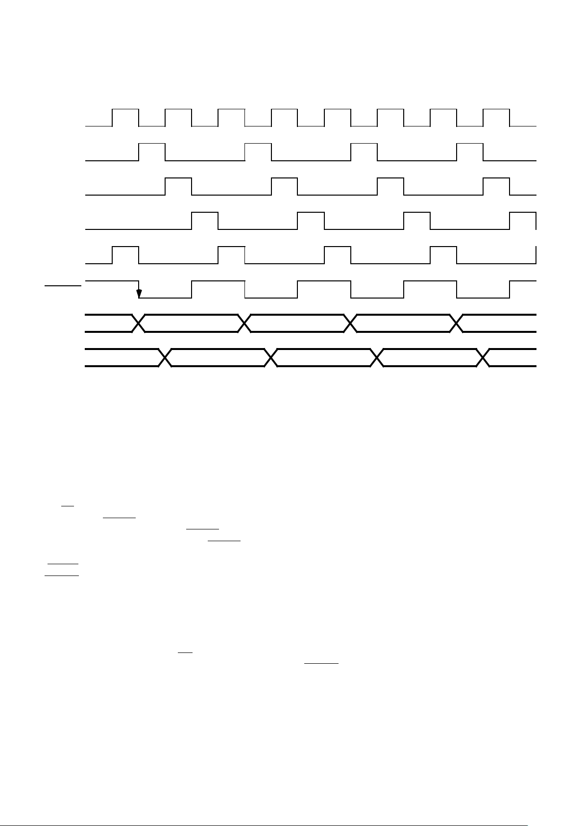
The UT69R000 divides all operations into four distinct time
periods (CK1 through CK4). These time periods are based on
the processor clock. The UT69R000 performs a separate
function during each of these four time periods.
During CK1, the UT69R000 begins executing the instruction
in the Primary Instruction Register (PIR). The instruction
executed is the instruction the UT69R000 fetched during the
previous bus cycle. Also during CK1, the instruction address
for the next instruction to fetch from memory becomes valid.
(Thus, the overlapping fetch and execute cycles of the
UT69R000.) STATE1 output goes low, indicating the
UT69R000 is executing an instruction.
The UT69R000 begins variable width clock period CK2 after
completing CK1. For 2 and 3 clock cycle instructions CK2
remains one-half clock cycle in length. During four clock cycle
instructions CK2 is stretched to one and a half clock cycles.
The following conditions extend time period CK2: (1)
Executing a STRI instruction, (2) Executing a LRI instruction,
or (3) Executing any instruction access to the operand port. The
UT69R000 also extends clock period CK2 for the Operand Port
arbitration process. The UT69R000 samples the logical AND
combination of BUSY and inverted BGNT during CK2. If this
combination is low, time period CK2 extends until the
combination of the two signals is high, indicating the
UT69R000 now controls the Operand Port. STATE1 output
remains low for the entire CK2 time period.
At the beginning of CK3, STATE1 goes high indicating the
next instruction is being fetched from memory. The
UT69R000’s operand address and data buses become active at
the beginning of CK3 along with the Bus Grant Acknowledge
(BGACK), M/IO, and R/WR signals. Data Strobe (DS) asserts
one clock cycle after the beginning of CK3, one and a half clock
cycles after the start of CK4.
Following CK3 is variable length clock period CK4. The
stretch of CK4 occurs during the following instruction
executions: (1) Executing a STRI instruction, (2) Executing a
LRI instruction, (3) Executing any instruction with Long
Immediate data (e.g., MOV Rd, FFFFh), or (4) Executing any
operand port access. After time period CK4 starts, the
transparent latches that make up the Primary Instruction
Register enable, allowing the UT69R000 to input the
instruction from memory.
17
If the instruction being executed requires access to the operand
bus, DS goes active. The UT69R000 samples the Data Transfer
Acknowledge (DTACK) on the next and every subsequent
rising edge of the processor clock. If DTACK is not low, the
UT69R000 extends time period CK4 until DTACK becomes
active or until an error condition is detected -- either Bus Error
(BTERR) or Memory Protect (MPROT) becomes active.
STATE1 remains high during the entire CK4 time period.
Figures 15, 16, and 17 show the timing relationships for CK1,
CK2, CK3, and CK4 during 2, 3, and 4 clock cycle instructions.
3.1 Instruction Port Operations
Most applications dedicate the instruction port to program
information. For these applications WE is always negated. The
UT69R000 can manipulate the instruction port through
instructions Store Register to Instruction Memory (STRI, write
access) and Load Register from Instruction Memory (LRI, read
access). Section 3.1.1 and 3.1.2 review the STRI and LRI
instructions.
3.1.1 STRI Instruction Bus Cycle
During an STRI instruction, instruction data moves from the
UT69R000 to the instruction memory. Figure 18 shows the
timing diagram of the signal relationships for the UT69R000
during STRI Instruction Bus Cycle Operation. Before the
UT69R00 executes the STRI instruction, the system
programmer must load the Accumulator Register with the
address which will receive the data. When the ACC is loaded
with the address information, the UT69R000 can begin
executing the STRI instruction.
Executing the STRI instruction begins when the falling edge
of OSCIN signals the start of time period CK1. At the beginning
of CK1, the data previously stored in the ACC becomes a valid
address on the instruction port address bus (RA(19:0)) and
STATE1 output becomes active, indicating the UT69R000 is
executing an instruction.
OSCIN
CK1
CK2
CK3
STATE1
EXECUTE FETCH
Figure 15. Machine Cycle 1 (2 Clock Cycle Instructions)
CK4
RA(19:0)
RD(15:0)
Valid Address Valid Address Valid Address
Instruction Data Instruction Data Instruction Data
18
3.1.2 LRI Instruction Bus Cycle
During an LRI instruction, the UT69R000 moves the
instruction data from the instruction memory to the
UT69R000.Figure 19 shows the timing diagram of the signal
relationships for the UT69R000 during an LRI Instruction Bus
Cycle.
Just as with the STRI instruction, before the UT69R000
executes the LRI instruction the system programmer must load
the UT69R000’s accumulator with the address from which the
data will be read. After the ACC is loaded with the address
information, LRI instruction execution can take place.
OSCIN
CK1
CK2
CK3
CK4
Figure 16. Machine Cycle 2 (3 Clock Cycle Instructions)
STATE1
EXECUTE FETCH
RA(19:0)
RD(15:0)
Note:
1. Examples of three clock cycle instructions include (operand port accesses):
LR Rd, Rs
STR Rd, Rs
STATUS
DS
A(15:0)
D(15:0)
Address Valid
Data Read
Control Valid
Fetch Address Valid
Fetch Instruction
Fetch Address Valid
Fetch Instruction
(M/IO, R/WR)
19
Executing the LRI instruction begins when the falling edge of
OSCIN signals the start of time period CK1. At the beginning
of CK1, the data previously stored in the ACC becomes a valid
address on the instruction port address bus (RA(19:0)) and
STATE1 output becomes active indicating the UT69R000 is
executing an instruction.
The data on the data bus is read into the UT69R000 during time
period CK2. The function of the remainder of the bus cycle
(time periods CK3 and CK4) is the same as for other
instructions. STATE1 is high, indicating the next instruction
is being fetched from memory and is ready for execution during
the next bus cycle.
4.0 Operand Port
The UT69R000 Operand Data bus interface supports multiple
processor and direct memory access (DMA) configurations.
The Operand Address bus A(15:0), data bus D(15:0), and
memory control bus signals (DS, R/WR, and M/IO) are TTLcompatible outputs that may be placed in a high-impedance
state. These signals are only active during bus cycles when the
UT69R000 is the current bus master. On other bus cycles, these
signals enter a high-impedance state so an alternate bus master
can control the port.
OSCIN
CK1
CK2
CK3
CK4
STATE1
Figure 17. Machine Cycle 3 (4 Clock Cycle Instructions)
EXECUTE
RA(19:0)
RD(15:0)
Note:
1. Examples of three clock cycle instructions include (long immediate accesses):
MOV Rd, FFFF (hex)
ADD Rd, FFFF (hex)
STATUS
DS
A(15:0)
D(15:0)
Address Valid
Data Read
Control Valid
Fetch Address Valid
Fetch Instruction
Immediate Address
Immediate Data
FETCH
Fetch Address Valid
Fetch Instruction
(M/IO, R/WR)
 Loading...