

UTMC 5962R9684504VXC, 5962R9684504VXA, 5962R9684504QYX, 5962R9684504QYC, 5962R9684504QYA Datasheet
...
FEATURES
q 45ns and 55ns maximum address access time
q Asynchronous operation for compatibility with industry-
standard 4K x 8/9 dual-port static RAM
q CMOS compatible inputs, TTL/CMOS compatible output
levels
q Three-state bidirectional data bus
q Low operating and standby current
q Radiation-hardened process and design; total dose
irradiation testing to MIL-STD-883 Method 1019
- Total-dose: 1.0E6 rads(Si)
- Memory Cell LET threshold: 85 MeV-cm2/mg
- Latchup immune (LET >100 MeV-cm2/mg)
q QML Q and QML V compliant part
q Packaging options:
- 68-lead Flatpack
- 68-pin PGA
q 5-volt operation
q Standard Microcircuit Drawing 5962-96845
INTRODUCTION
The UT7C138 and UT7C139 are high-speed radiationhardened CMOS 4K x 8 and 4K x 9 dual-port static RAMs.
Arbitration schemes are included on the UT7C138/139 to
handle situations when multiple processors access the same
memory location. Two ports provide independent,
asynchronous access for reads and writes to any location in
memory. The UT7C138/139 can be utilized as a stand-alone
32/36-Kbit dual-port static RAM or multiple devices can be
combined in order to function as a 16/18-bit or wider master/
slave dual-port static RAM. For applications that require
depth expansion, the BUSY pin is open-collector allowing
for wired OR circuit configuration. An M/ S pin is provided
for implementing 16/18-bit or wider memory applications
without the need for separate master and slave devices or
additional discrete logic. Application areas include
interprocessor/multiprocessor designs, communications,
and status buffering.
Each port has independent control pins: chip enable (CE),
read or write enable (R/ W), and output enable (OE). BUSY
signals that the port is trying to access the same location
currently being accessed by the other port.
Standard Products
UT7C138/139 4Kx8/9 Radiation-Hardened
Dual-Port Static RAM with Busy Flag
Data Sheet
January 2002
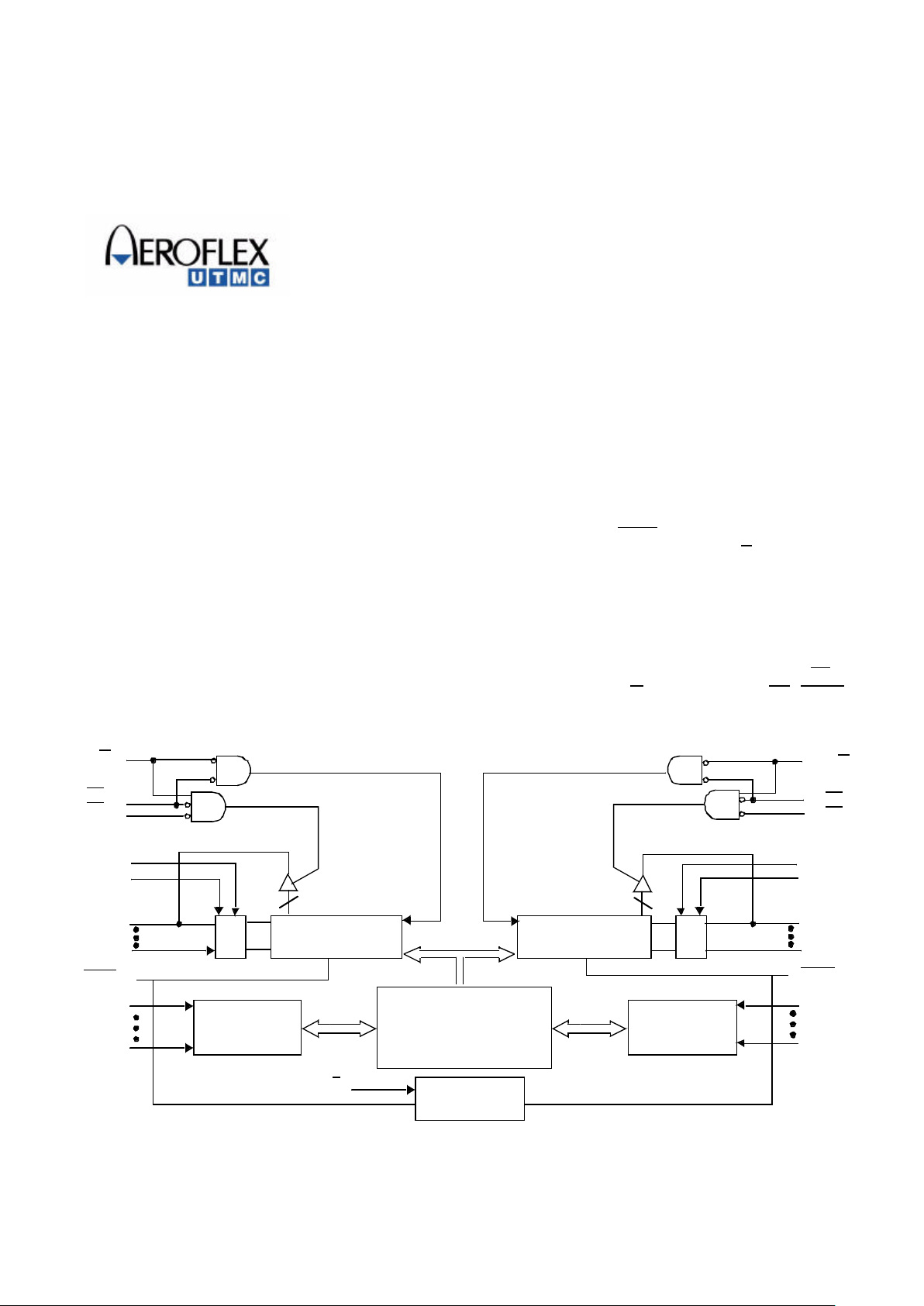
Figure 1. Logic Block Diagram
MEMORY
ARRAY
ROW
SELECT
ROW
SELECT
COL
SEL
COL
SEL
COLUMN
I/O
COLUMN
I/O
R/W
L
CE
L
OE
L
A
11L
A
10L
A
9L
A
0L
R/W
R
CE
R
OE
R
A
11R
A
10R
A
9R
A
0R
I/O
7L
I/O8L (7C139)
I/O
7R
I/O8R (7C139)
I/O
0L
I/O
0R
ARBITRATION
BUSY
L
BUSY
R
M/S
2
60
59
58
57
56
55
54
53
52
51
50
49
48
47
46
45
44
27
28
29
30
31
32
33
34
35
36
37
38
39
40
41
42
43
9
8
7
6
5
4
3
2
1
68
67
66
65
64
63
62
61
7C138/139
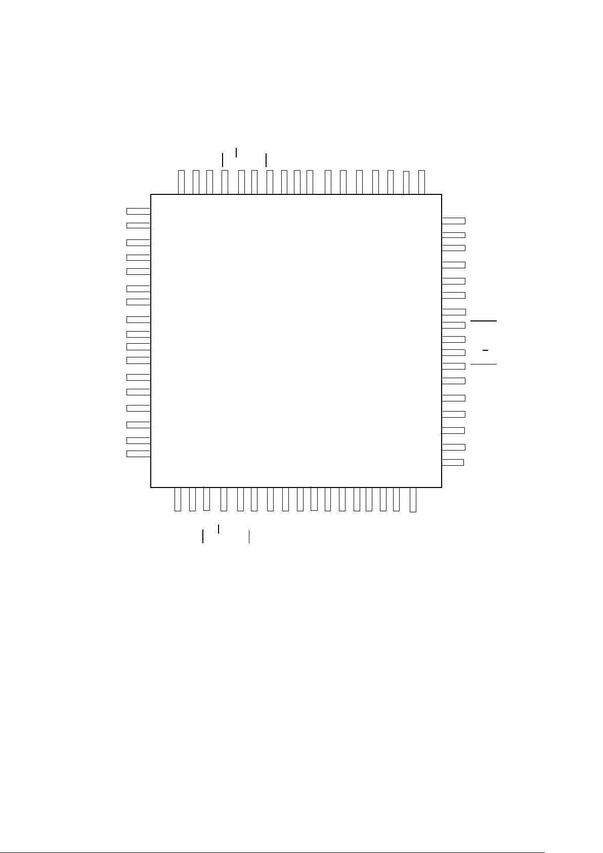
Figure 2a. DPRAM Pinout (68-Flatpack)
(top view)
A
5L
A
4L
A
3L
A
2L
A
1L
A
0L
NC
BUSY
L
GND
M/S
BUSY
R
NC
A
0R
A
1R
A
2R
A
3R
A
4R
I/O
7R
NC
(1)OER
R/WRNC
CERNC
NC
GND
NC
A
11RA10RA9RA8RA7RA6RA5R
I/O1LI/O0LNC
(2)
OE
R/WLNC
CELNC
NC
VDDNC
A11LA10LA9LA8LA7LA6
L
10
11
12
13
14
15
16
17
18
19
20
21
22
23
24
25
26
I/O
2L
I/O
3L
I/O
4L
I/O
5L
GND
I/O
6L
I/O
7L
V
DD
GND
I/O
0R
I/O
1R
I/O
2R
V
DD
I/O
3R
I/O
4R
I/O
5R
I/O
6R
Notes:
1. I/O8R on the7C139
2. I/O8L on the 7C139
3
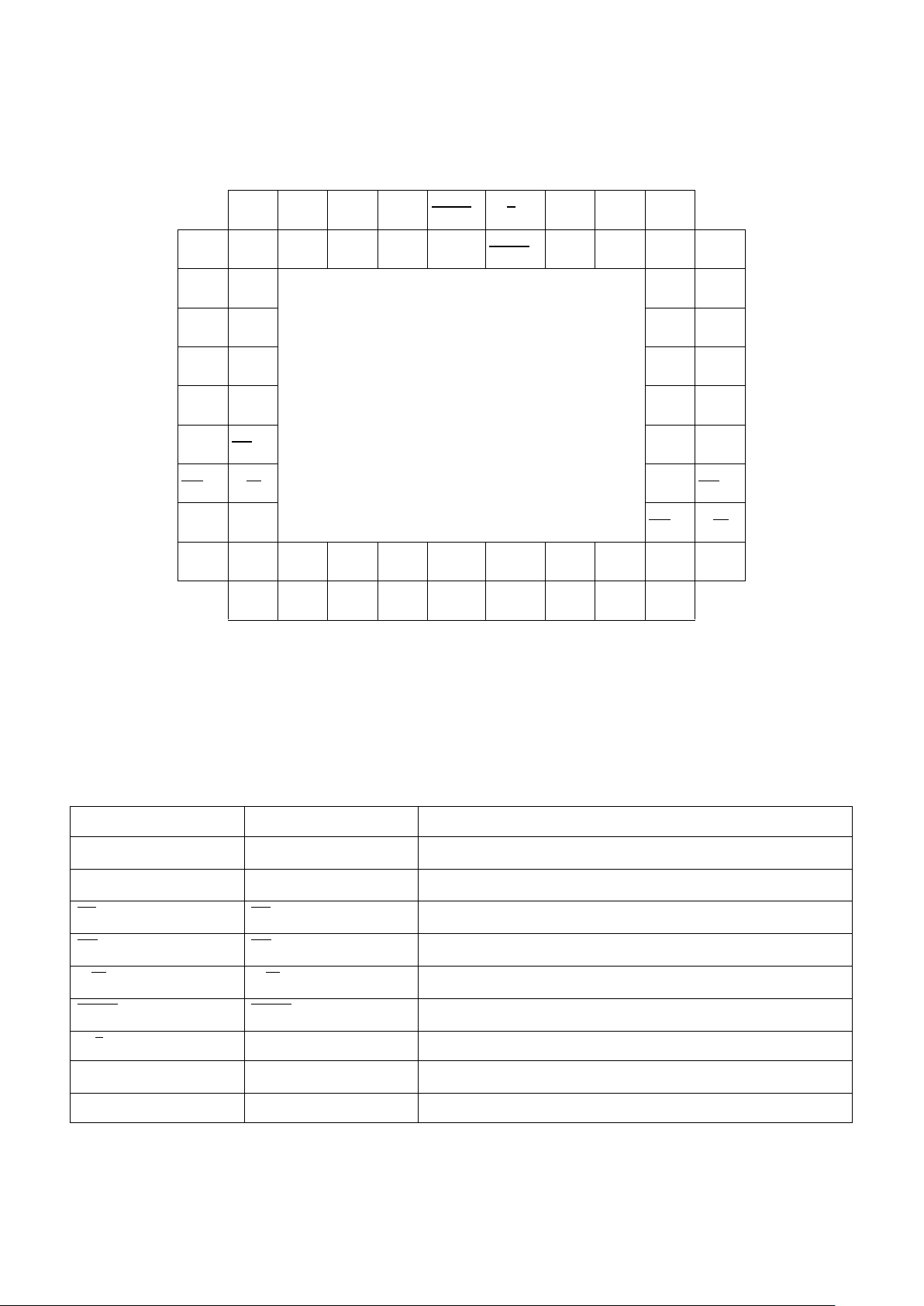
Figure 2b: DPRAM Pinout (68 PGA)
(top view)
Notes:
1. I/O8R on the7C139
2. I/O8L on the 7C139
PIN NAMES
B11
A
5L
C11
A
4L
D11
A
2L
E11
A
0L
F11
BUSY
L
G11
M/S
H11NCJ11
A
1R
K11
A
3R
A10
A
7L
B10
A
6L
C10
A
3L
D10
A
1L
E10NCF10
GND
G10
BUSY
R
H10
A
0R
J10
A
2R
K10
A
4R
L10
A
5R
A9
A
9L
B9
A
8L
K9
A
7R
L9
A
6R
A8
A
11L
B8
A
10L
K8
A
9R
L8
A
8R
A7
V
DD
B7
NC
K7
A
11R
L7
A
10R
A6
NCB6NC
K6
GNDL6NC
A5
NCB5CE
L
K5NCL5
NC
A4
OE
L
B4
R/W
L
K4NCL4
CE
R
A3
I/O
0L
B3
NC
(2)
K3
OE
R
L3
R/W
R
A2
I/O
1L
B2
I/O
2L
C2
I/O
4L
D2
GNDE2I/O
7L
F2
GNDG2I/O
1R
H2
V
DD
J2
I/O
4R
K2
I/O
7R
L2
NC
(1)
B1
I/O
3L
C1
I/O
5L
D1
I/O
6L
E1
V
DD
F1
I/O
0R
G1
I/O
2R
H1
I/O
3R
J1
I/O
5R
K1
I/O
6R
LEFT PORT RIGHT PORT DESCRIPTION
I/O
0L-7L(8L)
I/O
0R-7R(8R)
Data Bus Input/Output
A
0L-11L
A
0R-11R
Address Lines
CE
L
CE
R
Chip Enable
OE
L
OE
R
Output Enable
R/W
L
R/W
R
Read/Write Enable
BUSY
L
BUSY
R
Busy Flag Input/Output
M/S Master or Slave Select
V
DD
Power
GND Ground
7C138/139
11
10
9
8
7
6
5
4
3
2
1
A B C D E F H J K LG
4
The UT7C138/139 consists of an array of 4K words of 8 or 9
bits of dual-port SRAM cells, I/O and address lines, and control
signals (CE, OE, R/W). These control pins permit independent
access for reads or writes to any location in memory. To handle
simultaneous writes/reads to the same location, a BUSY pin is
provided on each port. With the M/S pin, the UT7C138/139 can
function as a master (BUSY pins are outputs) or as a slave
(BUSY pins are inputs). Each port is provided with its own
output enable control (OE), which allows data to be read from
the device.
WRITE CYCLE
A combination of R/W less than VIL (max), and CE less than
VIL (max), defines a write cycle. The state of OE is a “don’t
care” for a write cycle. The outputs are placed in the high-
impedance state when either OE is greater than VIH (min), or
when R/W is less than VIL (max).
WRITE OPERATION
Write Cycle 1, the Write Enable-controlled Access shown in
figure 4a, is defined by a write terminated by R/W going high
with CE active. The write pulse width is defined by t
PWE
when
the write is initiated by R/W, and by t
SCE
when the write is
initiated by CE going active. Unless the outputs have been
previously placed in the high-impedance state by OE, the user
must wait t
HZOE
before applying data to the eight/nine
bidirectional pins I/O(0:7/0:8) to avoid bus contention.
Write Cycle 2, the Chip Enable-controlled Access shown in
figure 4b, is defined by a write terminated by CE going inactive.
The write pulse width is defined by t
PWE
when the write is
initiated by R/ W, and by t
SCE
when the write is initiated by CE
going active. For the R/ W initiated write, unless the outputs have
been previously placed in the high-impedance state by OE, the
user must wait t
HZWE
before applying data to the eight/nine
bidirectional pins I/O(0:7/0:8) to avoid bus contention.
If a location is being written by one port and the opposite port
attempts to read that location, a port-to-port flow through delay
must be met before the data is read on the output. Data will be
valid on the port wishing to read the location (t
BZA
+ t
BDD
) after
the data is written on the other port (see figure 5a).
READ OPERATION
When reading the device, the user must assert both the OE and
CE pins. Data will be available t
ACE
after CE or t
DOE
after OE
is asserted (see figures 3a and 3b).
MASTER/SLAVE
A M/ S pin is provided in order to expand the word width by
configuring the device as either a master or a slave. The BUSY
output of the master is connected to the BUSY input of the slave.
Writing of slave devices must be delayed until after the BUSY
input has settled. Otherwise, the slave chip may begin a write
cycle during a contention situation. When presented as a HIGH
input, the M/S pin allows the device to be used as a master and,
therefore, the BUSY line is an output. BUSY can then be used
to send the arbitration outcome to a slave. When presented as a
LOW input, the M/S pin allows the device to be used as a slave,
and, therefore, the BUSY pin is an input.
Table 1. Non-Contending Read/Write
RADIATION HARDNESS
The UT7C138/139 incorporates special design and layout
features which allow operation in high-level radiation
environments. UTMC has developed special low-temperature
processing techniques designed to enhance the total-dose
radiation hardness of both the gate oxide and the field oxide
while maintaining the circuit density and reliability. For
transient radiation hardness and latchup immunity, UTMC
builds all radiation-hardened products on epitaxial wafers using
an advanced twin-tub CMOS process. In addition, UTMC pays
special attention to power and ground distribution during the
design phase, minimizing dose-rate upset caused by rail
collapse.
Table 2. Radiation Hardness
Design Specifications
1
Notes:
1. The DPRAM will not latchup during radiation exposure under recommended
operating conditions.
2. Not tested for CMOS technology.
INPUTS OUTPUTS
CE R/W OE I/O
0-7
OPERATION
H X X High Z Power Down
X X H High Z I/O Lines
Disabled
L H L Data Out Read
L L X Data In Write
L X X --- Illegal
Condition
Total Dose 1.0E6 rads(Si)
LET Threshold 85
MeV-cm2/mg
Neutron Fluence
2
3.0E14
n/cm
2
Memory Device
Cross Section @ LET
= 120MeV-cm2/mg
< 1.376E-2 (4Kx8)
< 1.548E-2 (4Kx9)
cm
2
5
ABSOLUTE MAXIMUM RATINGS
1
(Referenced to VSS)
Notes:
1. Stresses outside the listed absolute maximum ratings may cause permanent damage to the device. This is a stress rating only, and functional operation of the device
at these or any other conditions beyond limits indicated in the operational sections of this specification is not recommended. Exposure to absolute maximum rating
conditions for extended periods may affect device reliability.
2. Maximum junction temperature may be increased to +175°C during burn-in and steady-static life.
3. Test per MIL-STD-883, Method 1012, infinite heat sink.
RECOMMENDED OPERATING CONDITIONS
SYMBOL PARAMETER LIMITS
V
DD
DC supply voltage -0.5 to 7.0V
V
I/O
Voltage on any pin -0.5 to (V
DD
+ 0.3)V
T
STG
Storage temperature -65 to +150 °C
P
D
Maximum power dissipation 2.0W
T
J Maximum junction temperature
2
+150°C
Θ
JC Thermal resistance, junction-to-case
3
3.3°C/W
I
I
DC input current
±10 mA
SYMBOL PARAMETER LIMITS
V
DD
Positive supply voltage 4.5 to 5.5V
T
C
Case temperature range -55 to +125°C
V
IN
DC input voltage 0V to V
DD
6
DC ELECTRICAL CHARACTERISTICS (Pre/Post-Radiation )*
(VDD = 5.0V ±10%; -55°C < TC < +125 °C)
Notes:
* Post-radiation performance guaranteed at 25°C per MIL-STD-883 Method 1019.
1. Measured only for initial qualification and after process or design changes that could affect input/output capacitance.
2. Supplied as a design limit but not guaranteed or tested.
3. Not more than one output may be shorted at a time for maximum duration of one second.
4. VIH = 5.5V, VIL = 0V.
5. IDD (OP) derates at 6.4mA/MHz.
6. IDD (OP) derates at 3.4mA/MHz.
SYMBOL PARAMETER CONDITION MIN MAX UNIT
V
IH
High-level input voltage (CMOS) 0.7V
DD
V
V
IL
Low-level input voltage (CMOS) 0.3V
DD
V
V
OL
Low-level output voltage IOL = 8mA, V
DD
= 4.5V (TTL) 0.4 V
V
OL
Low-level output voltage IOL = 200µA, VDD = 4.5V (CMOS) 0.05 V
V
OH
High-level output voltage IOH = -4mA, VDD = 4.5V (TTL) 2.4 V
V
OH
High-level output voltage IOH = -200µA, VDD = 4.5V (CMOS) 4.45 V
C
IN
1
Input capacitance ƒ = 1MHz @ 0V 25 pF
C
IO
1
Bidirectional I/O capacitance ƒ = 1MHz @ 0V 25 pF
I
IN
Input leakage current VIN = VDD and V
SS
-10 10 µA
I
OZ
Three-state output leakage current VO = VDD and V
SS
VDD = 5.5V
G = 5.5V
-10 10 µA
I
OS
2,3
Short-circuit output current VDD = 5.5V, VO = V
DD
VDD = 5.5V, VO = 0V
-90
90 mA
mA
IDD(OP)
4,5
Supply current operating (both ports)
@ 22.2MHz
CMOS inputs (I
OUT
= 0)
VDD = 5.5V
300 mA
IDD(OP)
4,6
Supply current operating (single port)
@ 22.2 MHz
CMOS inputs (I
OUT
= 0)
VDD = 5.5V
150 mA
IDD(OP)
4,5
Supply current operating (both ports)
@ 18.2MHz
CMOS inputs (I
OUT
= 0)
VDD = 5.5V
275 mA
IDD(OP)
4,6
Supply current operating (single port)
@ 18.2 MHz
CMOS inputs (I
OUT
= 0)
VDD = 5.5V
138 mA
IDD(SB)
4
Supply current standby CMOS inputs (I
OUT
= 0)
CE = V
DD
- 0.5, V
DD
= 5.5V
1 mA
7
AC CHARACTERISTICS READ CYCLE
1,2
(VDD = 5.0V±10%)
Notes:
1. Test conditions assume signal transition time of 5ns or less, timing reference levels of VDD/2, input pulse levels of 0.5V to VDD-0.5V, and output
loading of the specified IOL/IOH and 50-pF load capacitance.
2. AC test conditions use VOH/VOL=VDD/2 + 500mV.
SYMBOL PARAMETER
7C138 - 45
7C139 - 45
MIN MAX
7C138 - 55
7C139 - 55
MIN MAX
UNIT
t
RC
Read cycle time 45 55 ns
t
AA
Address to data valid
2
45 55 ns
t
OHA
Output hold from address change 5 5 ns
t
ACE
CE LOW to data valid
2
45 55 ns
t
DOE
OE LOW to data valid
2
20 20 ns
t
LZOE
OE LOW to low Z 0 0 ns
t
HZOE
OE HIGH to high Z 20 20 ns
t
LZCE
CE LOW to low Z 0 0 ns
t
HZCE
CE HIGH to high Z 20 20 ns
 Loading...