

UTMC 5962R8864406ZX, 5962R8864406ZA, 5962R8864406YX, 5962R8864406XC, 5962R8864406XA Datasheet
...
1
Standard Products
UT63M1XX MIL-STD-1553A/B Bus Transceiver
Data Sheet
Sept. 1999
FEATURES
q Full conformance to MIL-STD-1553A and 1553B
q Completely monolithic bipolar technology
q Low power consumption
q Fit and functionally compatible to industry standard 631XX
series
q Idle low encoding version
q Flexible power supply voltages: VCC=+5V, VEE=-12V or -
15V, and V
CCA
=+5V to +12V or +5V to +15V
q Full military operating temperature range, -55°C to +125°C,
screened to QML Q or QML V requirements
q Standard Military Drawing available
INTRODUCTION
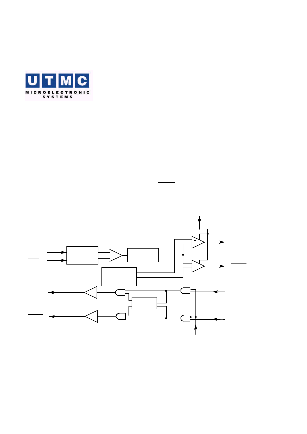
The monolithic UT63M1XX Transceivers are complete
transmitter and receiver pairs conforming fully to MIL-STD-
1553A and 1553B. Encoder and decoder interfaces are idle low.
UTMC’s advanced bipolar technology allows the positive
analog power to range from +5V to +12V or +5V to +15V,
providing more flexibility in system power supply design.
The receiver section of the UT63M1XX series accepts biphasemodulated Manchester II bipolar data from a MIL-STD-1553
data bus and produces TTL-level signal data at its RXOUT and
RXOUT outputs. An external RXEN input enables or disables
the receiver outputs.
TXIN
RXOUT
RXEN
FROM ENCODER
TO DECODER
DRIVERS
COMPARE
FILTER
LIMITER
and
FILTER
TXIHB
Figure 1. Functional Block Diagram
RXIN
TXOUT
RXIN
TXOUT
RXOUT
TXIN
THRESHOLD
REFERENCE
2
Legend for TYPE field:
TI = TTL input
TO = TTL output
DO = Differential output
DI = Differential input
() = Channel designator
TRANSMITTER
NAME PACKAGE PIN TYPE DESCRIPTION
SINGLE DUAL
TXOUT
(A)
1 1 DO Transmitter outputs: TXOUT and TXOUT are differential data signals.
TXOUT
(B)
N/A 10 DO
TXOUT
(A)
2 2 DO
TXOUT is the complement of TXOUT.
TXOUT
(B)
N/A 11 DO
TXIHB
(A)
21 34 TI
Transmitter inhibit: this is an active high input signal.
TXINB
(B)
N/A 25 TI
TXIN
(A)
22 35 TI Transmitter inputs: TXIN and TXIN are complementary TTL-level
Manchester II encoder inputs.
TXIN
(B)
N/A 26 TI
TXIN
(A)
23 36 TI TXIN is the complement of TXIN input.
TXIN
(B)
N/A 27 TI
The transmitter section accepts biphase TTL-level signal data
at its TXIN and TXIN and produces MIL-STD-1553 data
signals. The transmitter’s output voltage is typically 42VPP, L-
L. Activating the TXIHB input or setting both data inputs to
the same logic level disables the transmitter.
The UT63M1XX series offers a monolithic transmitter and
receiver packaged in either single channel (24-pin) or dualchannel (36-pin) configurations designed for use in any MILSTD-1553 application.
3
RECEIVER
NAME PACKAGE PIN TYPE DESCRIPTION
SINGLE DUAL
RXOUT
(A)
7 5 TO
Receiver outputs: RXOUT and RXOUT are complementary
Manchester II decoder outputs.
RXOUT
(B)
N/A 14 TO
RXOUT
(A)
10 8 TO
RXOUT is the complement of RXOUT output
RXOUT
(B)
N/A 17 TO
RXEN
(A)
8 6 TI
Receiver enable/disable: This is an active high input signal.
RXEN
(B)
N/A 15 TI
RXIN
(A)
15 29 DI
Receiver inputs: RXIN and RXIN are biphase-modulated Manchester
II bipolar inputs from MIL-STD-1553 data bus.
RXIN
(B)
N/A 20 DI
RXIN
(A)
16 30 DI
RXIN is the complement of RXIN input.
RXIN
(B)
N/A 21 DI
POWER AND GROUND
NAME PACKAGE PIN TYPE DESCRIPTION
SINGLE DUAL
V
CC
(A)
20 33 PWR
+5VDC power (±10%)
V
CC
(B)
N/A 24 PWR
V
CCA
(A)
13 28 PWR +5 to +12VDC power or
+5 to +15V
DC
power (± 5%)
V
CCA
(B)
N/A 19 PWR
V
EE
(A)
19 32 PWR -12 or -15VDC power (± 5%)
Recommended de-coupling capacitors 4.7µF and.1µF
V
EE
(B)
N/A 23 PWR
GND
(A)
3, 9, 18 3, 7, 31 GND
Ground reference
GND
(B)
N/A 12, 16, 22 GND
4
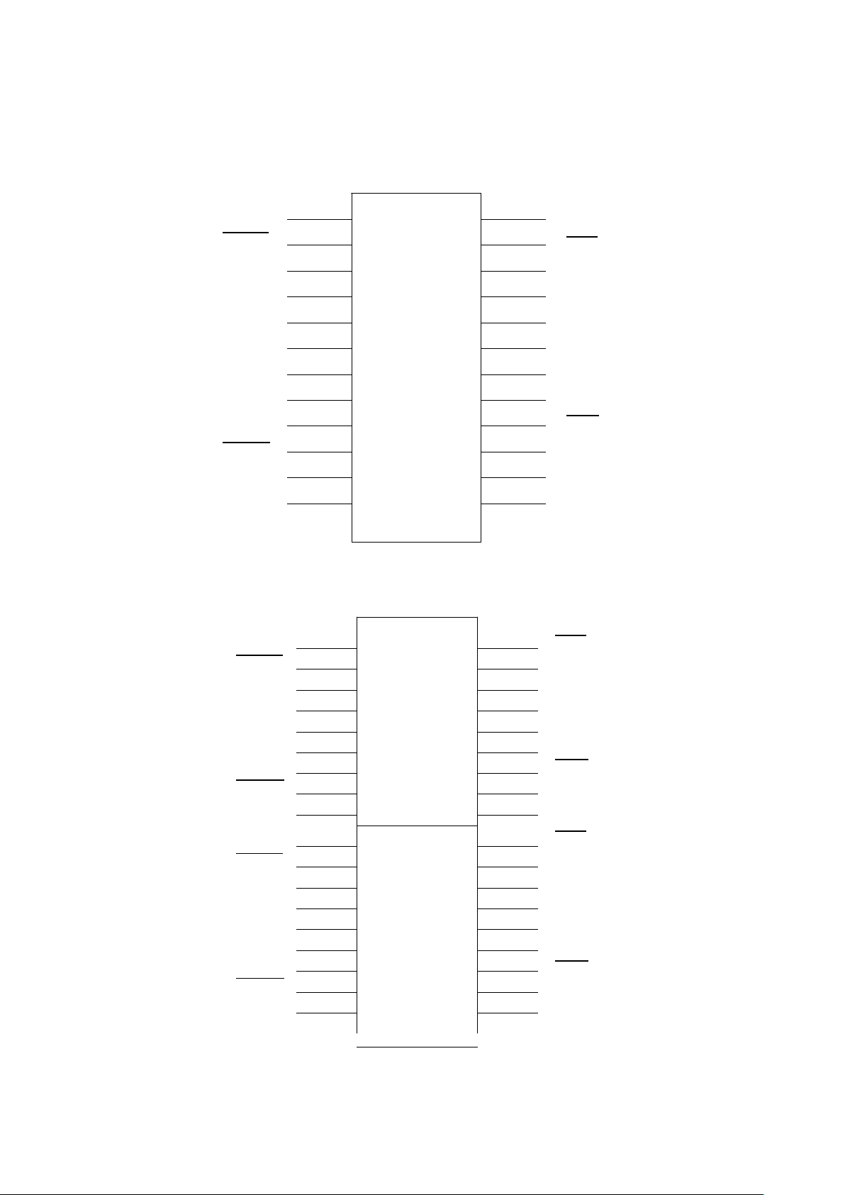
RXEN
RXOUT
TXOUT
RXIN
TXIN
24
23
22
21
20
19
18
17
16
15
14
1312
11
10
9
8
7
6
5
4
3
2
1
NC
NC
GND
NC
NC
NC
GND
NC
NC
GND
NC
CHANNEL
Figure 2a. Functional Pin Diagram--Single Channel
TXIHB
TXOUT
RXOUT
TXIN
RXIN
V
CCA
V
CC
V
EE
A
RXIN
TXIN
RXIN
TXIN
TXOUT
RXOUT
RXOUT
RXEN
RXEN
TXOUT 36
26
10
11
13
14
15
17
18
16
27
28
CHANNEL
35
34
33
32
31
30
29
26
25
24
23
22
B
21
20
19
CHANNEL
1
2
3
4
5
A
6
7
8
9
12
GND
GND
GND
NC
GND
NC
GND
NC
GND
NC
TXIHB
TXIHB
Figure 2b. Functional Pin Diagram--Dual Channel
TXOUT
RXOUT
TXIN
RXIN
TXOUT
RXIN
TXIN
RXOUT
V
CCA
V
CCA
V
CC
V
EE
V
CC
V
EE
5
TRANSMITTER
The transmitter section accepts Manchester II biphase TTL data
and converts this data into differential phase-modulated current
drive. Transmitter current drivers are coupled to a MIL-STD1553 data bus via a transformer driven from the TXOUT and
TXOUT terminals. Transmitter output terminals’ nontransmitting state is enabled by asserting TXIHB (logic 1), or
by placing both TXIN and TXIN at the same logic level. Table
1, Transmit Operating Mode, lists the functions for the output
data in reference to the state of TXIHB. Figure 3 shows typical
transmitter waveforms.
RECEIVER
The receiver section accepts biphase differential data from a
MIL-STD-1553 data bus at its RXIN and RXIN inputs. The
receiver converts input data to biphase Manchester II TTL
format and is available for decoding at the RXOUT and RXOUT
terminals. The outputs RXOUT and RXOUT represent positive
and negative excursions (respectively) of the inputs RXIN and
RXIN. Figure 4 shows typical receiver output waveforms.
Models UT63M105, UT63M107, UT63M125, and UT63M127
idle in the “0” state when disabled or receiving no signal.
POWER SUPPLY VOLTAGES
The UT63M1XX series meets device requirements over a wide
range of power supply voltages. Table 2 shows the overall
capabilities of all available devices. Each channel of the dual
transceiver is electrically and physically separate from the other
and fully independent, including all power and signal lines. Thus
there will be no interaction between the channels.
Notes:
1. x = Don’t care.
2. Transmitter output terminals are in the non-transmitting mode during Off
time.
3. Transmitter output terminals are in the non-transmitting mode during Off
time, independent of TXIHB status.
Table 1. Transmit Operating Mode
TXIN TXIN TXIHB TXOUT
x
1
x 1 Off
2
0 0 x Off
3
0 1 0 On
1 0 0 On
1 1 x Off
3
TXIN
Figure 3. Typical Transmitter Waveforms
TXIN
t
TXDD
90%
10%
TXOUT, TXOUT
TXIN
LINE-TO-LINE
DIFFERENTIAL
OUTPUT
TXIN
TXIHB
BOTH HIGH
OR
BOTH LOW
6
DATA BUS INTERFACE
The designer can connect the UT63M1XX to the data bus via a
short-stub (direct-coupling) connection or a long-stub
(transformer-coupling) connection. Use a short-stub connection
when the distance from the isolation transformer to the data bus
does not exceed a one-foot maximum. Use a long-stub
connection when the distance from the isolation transformer
exceeds the one-foot maximum and is less than twenty-five feet.
Figure 5 shows various examples of bus coupling
configurations. The UT63M1XX series transceivers are
designed to function with MIL-STD-1553A and 1553B
compatible transformers.
RECOMMENDED THERMAL PROTECTION
All packages, single and dual, should mount to or contact a heat
removal rail located in the printed circuit board. To insure proper
heat transfer between the package and the heat removal rail, use
a thermally conductive material between the package and the
heat removal rail. Use a material such as Mereco XLN-589 or
equivalent to insure heat transfer between the package and heat
removal rail.
Figure 4. Typical Receiver Waveforms
QUIESCENT IDLE LOW
RXOUT
RXOUT
LINE-TO-LINE
DIFFERENTIAL
INPUT
RXOUT
RXOUT
t
RXDD
Table 2. Transceiver Model Capabilities
MODEL V
CC
V
EE
V
CCA
IDLE
UT63M105 +5V -15V +5 to +15V
Low
UT63M107 +5V -12V +5 to +12V
Low
UT63M125 +5V -15V +5 to +15V
Low
UT63M127 +5V -12V +5 to +12V
Low

7
20 FT MAX
Figure 5. Bus Coupling Configuration
OPERATION
55 OHMS
55 OHMS
1 FT MAX
SHORT-STUB
DIRECT COUPLING
LONG-STUB
TRANSFORMER COUPLING
1:1.4
OPERATION
55 OHMS
55 OHMS
1 FT MAX
20 FT MAX
SHORT-STUB
DIRECT COUPLING
LONG-STUB
TRANSFORMER COUPLING
1.4:1
2:1 1:1.4
1.2:1
1.66:1
Note:
ZO defined per MIL-STD-1553B in section 4.5.1.5.2.1.
± 15V
DC
± 12V
DC
Z
O
.75Z
O
.75Z
O
Z
O
.75Z
O
.75Z
O
 Loading...