

UTMC 5962R0153601VYC, 5962R0153601VYA, 5962R0153601QYX, 5962H0153601VYX, 5962H0153601VYC Datasheet
...
1
FEATURES
q 400.0 Mbps low jitter fully differential data path
q 200MHz clock channel
q 3.3 V power supply
q 10mA LVDS output drivers
q Cold sparing all pins
q Fast propagation delay of 3.5ns max
q Receiver input threshold < + 100 mV
q Radiation-hardened design; total dose irradiation testing to
MIL-STD-883 Method 1019
- Total-dose: 300 krad(Si) and 1 Mrad(Si)
- Latchup immune (LET > 100 MeV-cm2/mg)
q Packaging options:
- 48-lead flatpack
q Standard Microcircuit Drawing 5962-01536
- QML Q and V compliant part
q Compatible with ANSI/TIA/EIA 644-1995 LVDS
Standard
INTRODUCTION
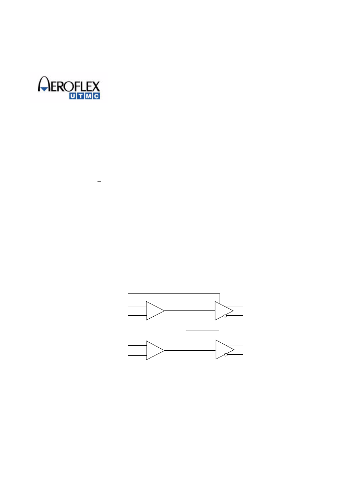
The UT54LVDM328 is an Octal Bus Repeater utilizing Low
Voltage Differential Signaling (LVDS) technology for low
power, high speed operation. Data paths are fully differential
from input to output for low noise generation and low pulse
width distortion. LVDS I/O enable high speed data transmission
for point-to point or multi-drop interconnects. This device is
designed for use as a high speed differential repeater.
The UT54LVDM328 is a repeater designed specifically for the
bridging of multiple backplanes in a system. The
UT54LVDM328 utilizes low voltage differential signaling to
deliver high speed while consuming minimal power with
reduced EMI. The UT54LVDM328 repeats signals between
backplanes and accepts or drives signals onto the local bus.
The individual LVDS outputs can be put into Tri-State by use
of the enable pins.
All pins have Cold Spare buffers. These buffers will be high
impedance when VDD is tied to VSS.
OUT1+
END
IN1+
+
-
OUT2+
IN2+
+
-
IN1-
OUT1-
OUT2-
IN2-
Standard Products
UT54LVDM328 Octal 400 Mbps Bus LVDS Repeater
Data Sheet
August, 2002
Figure 1a. UT54LVDM328 Repeater Block Diagram
(Partial - see Page 2 for complete diagram)
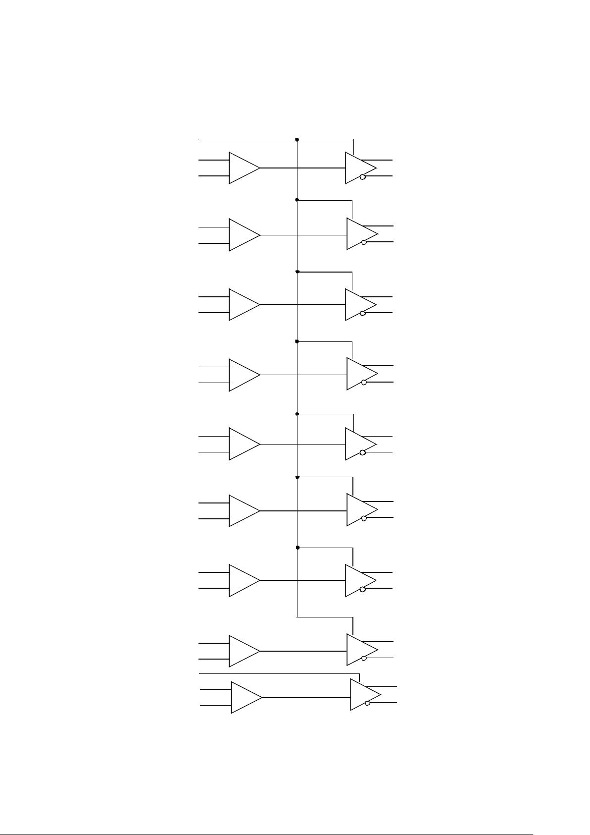
2
OUT1+
END
IN1+
+
-
OUT2+
IN2+
+
-
IN1-
OUT1-
OUT2-
IN2-
OUT3+
IN3+
+
-
OUT4+
IN4+
+
-
IN3-
OUT3-
OUT4-
IN4-
OUT5+
IN5+
+
-
OUT6+
IN6+
+
-
IN5-
OUT5-
OUT6-
IN6-
OUT7+
IN7+
+
-
OUT8+
IN8+
+
-
IN7-
OUT7-
OUT8-
IN8-
Clk In+
Clk Out+
+
-
Clk In-
Clk Out-
ENCK
Figure 1b. UT54LVDM328 Repeater Diagram
3
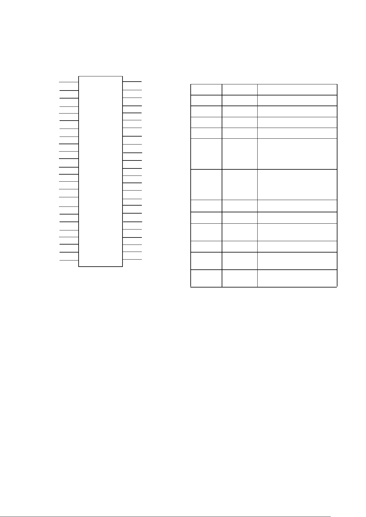
PIN DESCRIPTION
Figure 2. UT54LVDM328 Pinout
UT54LVDM328
Bus Repeater
48
47
46
45
44
43
42
41
OUT3+
1IN1+
2
3
4
5
6
7
8IN39
10
11
12
13
14
15
16
IN3+
CLK In+
CLK In-
IN5-
17
18
19
20
21
22
23
24
IN6-
VSS
IN8+
IN8-
OUT1+
VDD
40
39
38
37
36
35
34
33
CLK OUT-
OUT5-
VDD
CLK OUT+
32
31
30
29
28
27
26
25
OUT8-
OUT6+
OUT7+
IN1-
IN2-
VDD
IN4+
IN4-
ENCK
END
IN5+
IN6+
VDD
IN7+
IN7-
OUT1OUT2+
OUT2-
VSS
OUT3OUT4+
OUT4-
VSS
OUT5+
VSS
OUT6-
VDD
OUT7OUT8+
IN2+
VSS
Name # of Pins Description
INn+ 8 Non-inverting LVDS input
INn- 8 Inverting LVDS input
OUTn+ 8 Non-inverting LVDS output
OUTn- 8 Inverting LVDS Output
END 1 A logic low on the enable puts
the LVDS data output into Tri-
State and reduces the supply
current
ENCK 1 A logic low on the enable puts
the LVDS clock output into Tri-
State and reduces the supply
current
V
SS
5 Ground
V
DD
5 Power supply
CLK IN+ 1 Non-Inverting Clock LVDS
Input
CLK IN- 1 Inverting clock LVDS Input
CLK
OUT+
1 Non-Inverting Clock LVDS
Output
CLK
OUT-
1 Inverting Clock LVDS Output

4
APPLICATIONS INFORMATION
The UT54LVDM328 provides the basic bus repeater
function. The device operates as a 9 channel LVDS buffer.
Repeating the signal restores the LVDS amplitude, allowing
it to drive another media segment. This allows for isolation
of segments or long distance applications.
The intended application of these devices and signaling
technique is for both point-to-point baseband (single
termination) and multipoint (double termination) data
transmissions over controlled impedance media. The
transmission media may be printed-circuit board traces,
backplanes, or cables. (Note: The ultimate rate and distance
of data transfer is dependent upon the attenuation
characteristics of the media, the noise coupling to the
environment, and other application specific characteristics.)
Input Fail-Safe:
The UT54LVDM328 also supports OPEN, shorted and
terminated input fail-safe. Receiver output will be HIGH for
all fail-safe conditions.
PCB layout and Power System Bypass:
Circuit board layout and stack-up for the UT54LVDM328
should be designed to provide noise-free power to the device.
Good layout practice also will separate high frequency or high
level inputs and outputs to minimize unwanted stray noise
pickup, feedback and interference. Power system
performance may be greatly improved by using thin
dielectrics (4 to 10 mils) for power/ground sandwiches. This
increases the intrinsic capacitance of the PCB power system
which improves power supply filtering, especially at high
frequencies, and makes the value and placement of external
bypass capacitors less critical. External bypass capacitors
should include both RF ceramic and tantalum electrolytic
types. RF capacitors may use values in the range 0.01µF to
0.1µ F. Tantalum capacitors may be in the range of 2.2µF to
10µF. Voltage rating for tantalum capacitors should be at
least 5X the power supply voltage being used. It is
recommended practice to use two vias at each power pin of
the UT54LVDM328, as well as all RF bypass capacitor
terminals. Dual vias reduce the interconnect inductance and
extends the effective frequency range of the bypass
components.
The outer layers of the PCB may be flooded with additional
ground plane. These planes will improve shielding and
isolation, as well as increase the intrinsic capacitance of the
power supply plane system. Naturally, to be effective, these
planes must be tied to the ground supply plane at frequent
intervals with vias. Frequent via placement also improves
signal integrity in signal transmission lines by providing short
paths for image currents which reduces signal distortion. The
planes should be pulled back from all transmission lines and
component mounting pads a distance equal to the width of
the widest transmission line from the internal power or
ground plane(s) whichever is greater. Doing so minimizes
effects on transmission line impedances and reduces
unwanted parasitic capacitances at component mounting
pads.
Compatibility with LVDS standard:
In backplane multidrop configurations, with closely spaced
loads, the effective differential impedance of the line is
reduced. If the mainline has been designed for 50 Ω
differential impedance, the loading effects may reduce this
to the 35Ω range depending upon spacing and capacitance
load. Terminating the line with a 35Ω load is a better match
than with 50Ω and reflections are reduced.
5
ABSOLUTE MAXIMUM RATINGS
1
(Referenced to VSS)
Notes:
1. Stresses outside the listed absolute maximum ratings may cause permanent damage to the device. This is a stress rating only, and functional operation of the device
at these or any other conditions beyond limits indicated in the operational sections of this specification is not recommended. Exposure to absolute maximum rating
conditions for extended periods may affect device reliability and performance.
2. Maximum junction temperature may be increased to +175°C during burn-in and life test.
3. Test per MIL-STD-883, Method 1012.
4. For cold spare mode (VDD = VSS), V
I/O
may be -0.3V to the maximum recommended operating VDD +0.3V.
RECOMMENDED OPERATING CONDITIONS
SYMBOL PARAMETER LIMITS
V
DD
DC supply voltage -0.3 to 4.0V
V
I/O
Voltage on any pin -0.3 to (VDD + 0.3V)
T
STG
Storage temperature -65 to +150°C
P
D
Maximum power dissipation 800mW
T
J Maximum junction temperature
2
+150°C
Θ
JC
Thermal resistance, junction-to-case
3
22°C/W
I
I
DC input current
±10mA
SYMBOL PARAMETER LIMITS
V
DD
Positive supply voltage 3.3 to 3.6V
T
C
Case temperature range -55 to +125°C
V
IN
DC input voltage, receiver inputs 0 to 2.4V
DC input voltage, logic inputs 0 to VDD for END or ENCK
 Loading...