

UTMC 5962RTBD02VYX, 5962RTBD02VYC, 5962RTBD02VYA, 5962RTBD02QYX, 5962RTBD02QYC Datasheet
...
1
IN DEVELOP
M
E
NT
FEATURES
q >400.0 Mbps ( 200 MHz) switching rates
q +340mV differential signaling
q 3.3 V power supply
q TTL compatible outputs
q Cold spare all pins
q Nominal 105Ω Integrated Termination Resistor
q 3.3ns maximum propagation delay
q 0.35ns maximum differential skew
q Radiation-hardened design; total dose irradiation testing to
MIL-STD-883 Method 1019
- Total-dose: 300 krad(Si) and 1Mrad(Si)
- Latchup immune (LET > 100 MeV-cm2/mg)
q Packaging options:
- 16-lead flatpack (dual in-line)
q Standard Microcircuit Drawing TBD
- QML Q and V compliant part
q Compatible with IEEE 1596.3SCI LVDS
q Compatible with ANSI/TIA/EIA 644-1996 LVDS
Standard
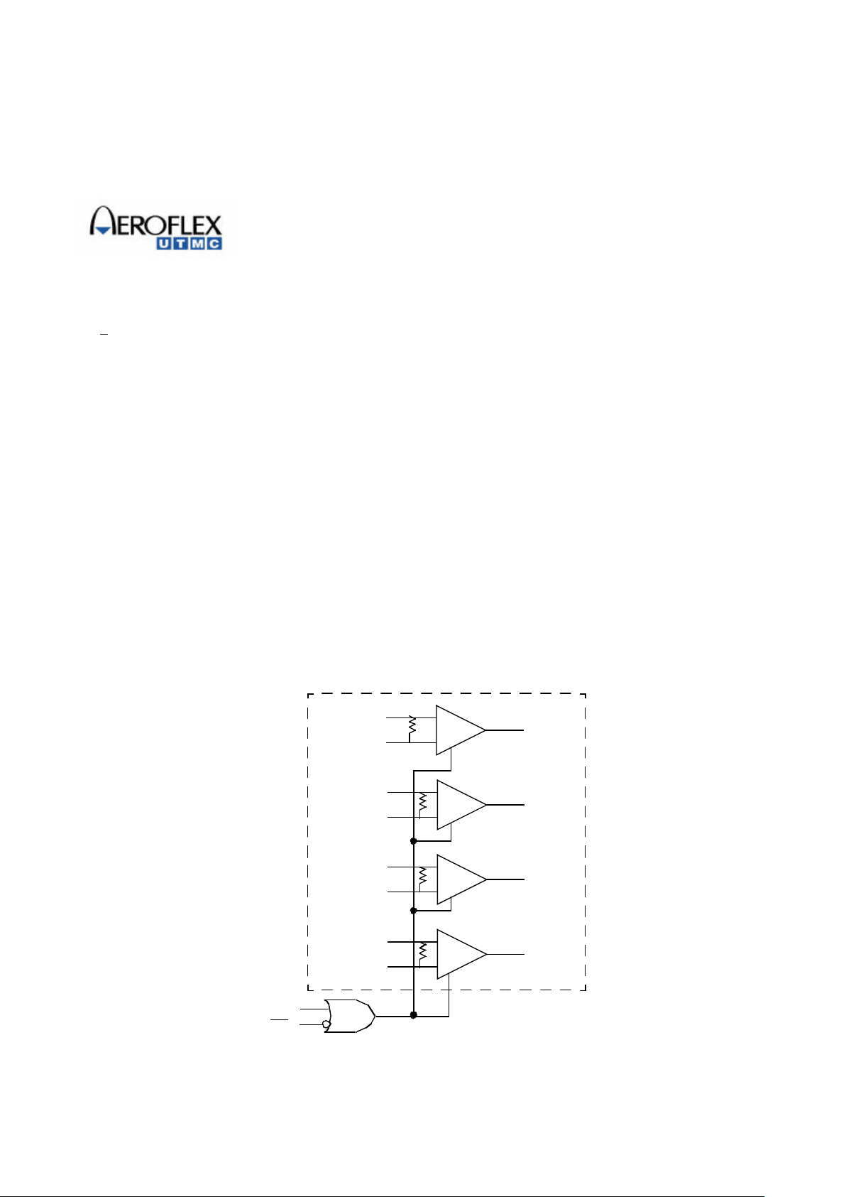
INTRODUCTION
The UT54LVDS032LV Quad Receiver is a quad CMOS
differential line receiver designed for applications requiring
ultra low power dissipation and high data rates. The device is
designed to support data rates in excess of 400.0 Mbps (200
MHz) utilizing Low Voltage Differential Signaling (LVDS)
technology.
The UT54LVDS032LV accepts low voltage (340mV)
differential input signals and translates them to 5V TTL output
levels. The receiver supports a three-state function that may be
used to multiplex outputs. The receiver also supports OPEN,
shorted and terminated (100 Ω) input fail-safe. Receiver output
will be HIGH for all fail-safe conditions.
The UT54LVDS032LV and companion quad line driver
UT54LVDS031LV provides new alternatives to high power
pseudo-ECL devices for high speed point-to-point interface
applications.
All pins have Cold Spare buffers. These buffers will be high
impedance when VDD is tied to VSS.
An integrated termination resistor will reduce component count
and save board space.
+
R1
-
R
IN1+
R
IN1-
R
IN2+
R
IN2-
R
IN3+
R
IN3-
R
IN4+
R
IN4-
R
OUT1
R
OUT2
R
OUT4
R
OUT3
EN
EN
+
R2
-
+
R3
-
+
R4
-
Standard Products
UT54LVDS032LVT Low Voltage Quad Receiver with Integrated
Termination Resistor
Preliminary Data Sheet
February 14, 2003
Figure 1. UT54LVDS032LV Quad Receiver Block Diagram
2
IN DEVELOP
M
E
NT
TRUTH TABLE
PIN DESCRIPTION
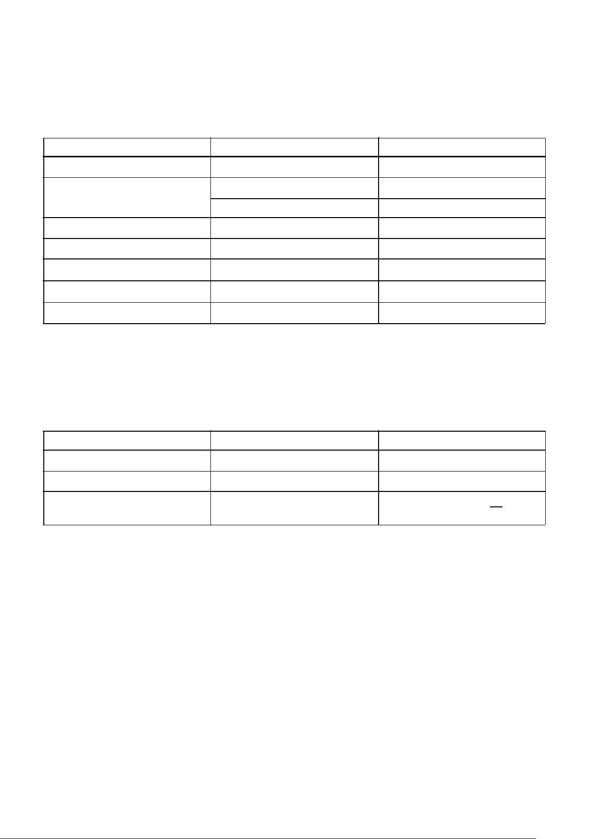
APPLICATIONS INFORMATION
The UT54LVDS032LVT receiver’s intended use is primarily in
an uncomplicated point-to-point configuration as is shown in
Figure 3. This configuration provides a clean signaling
environment for quick edge rates of the drivers. The receiver is
connected to the driver through a balanced media which may be
a standard twisted pair cable, a parallel pair cable, or simply
PCB traces. Typically, the characteristic impedance of the media
is in the range of 100Ω. An integrated termination resistor of
105Ω is used to match the media . The termination resistor
converts the current sourced by the driver into voltages that are
detected by the receiver. Other configurations are possible such
as a multi-receiver configuration, but the effects of a mid-stream
connector(s), cable stub(s), and other impedance discontinuities,
as well as ground shifting, noise margin limits, and total
termination loading must be taken into account.
The UT54LVDS032LVT differential line receiver is capable of
detecting signals as low as 100mV, over a + 1V common-mode
range centered around +1.2V. This is related to the driver offset
voltage which is typically +1.2V. The driven signal is centered
around this voltage and may shift +1V around this center point.
The +1V shifting may be the result of a ground potential
difference between the driver’s ground reference and the
receiver’s ground reference, the common-mode effects of
coupled noise or a combination of the two. Both receiver input
pins should honor their specified operating input voltage range
of 0V to +2.4V (measured from each pin to ground).
The integrated termination resistor is a nominal 105 Ω when VDD
is 3.0 to 3.6V. In cold spare mode, the integrated termination
resistor is 145Ω.
Enables Input Output
EN EN R
IN+
- RIN- R
OUT
L H X Z
All other combinations
of ENABLE inputs
VID > 0.1V H
VID < -0.1V L
Full Fail-safe
OPEN/SHORT or
Terminated
H
Pin No. Name Description
2, 6, 10, 14 R
IN+
Non-inverting receiver input pin
1, 7, 9, 15 R
IN-
Inverting receiver input pin
3, 5, 11, 13 R
OUT
Receiver output pin
4 EN Active high enable pin, OR-ed
with EN
12 EN Active low enable pin, OR-ed
with EN
16 V
DD
Power supply pin, +3.3 + 0.3V
8 V
SS
Ground pin
Figure 2. UT54LVDS032LVT Pinout
UT54LVDS032LV
Receiver
16
15
14
13
12
11
10
9
V
DD
R
IN4-
R
IN4+
R
OUT4
EN
R
OUT3
R
IN3+
R
IN3-
1
R
IN1-
2
R
IN1+
3
R
OUT1
4EN
5
R
OUT2
6
R
IN2+
7
R
IN2-
8
V
SS
ENABLE
DATA
INPUT
1/4 UT54LVDS031LV
1/4 UT54LVDS032LV
+
-
DATA
OUTPUT
Figure 3. Point-to-Point Application
RT 100 Ω

3
IN DE
VE
L
O
PMENT
Receiver Fail-Safe
The UT54LVDS032LVT receiver is a high gain, high speed
device that amplifies a small differential signal (20mV) to
TTL logic levels. Due to the high gain and tight threshold of
the receiver, care should be taken to prevent noise from
appearing as a valid signal.
The receiver’s internal fail-safe circuitry is designed to
source/sink a small amount of current, providing fail-safe
protection (a stable known state of HIGH output voltage) for
floating, terminated or shorted receiver inputs.
1. Open Input Pins. The UT54LVDS032LVT i s a quad
receiver device, and if an application requires only 1,
2 or 3 receivers, the unused channel(s) inputs should
be left OPEN. Do not tie unused receiver inputs to
ground or any other voltages. The input is biased by
internal high value pull up and pull down resistors to
set the output to a HIGH state. This internal circuitry
will guarantee a HIGH, stable output state for open
inputs.
2. Terminated Input. If the driver is disconnected
(cable unplugged), or if the driver is in a three-state
or power-off condition, the receiver output will again
be in a HIGH state, even with the end of cable 100 Ω
integrated termination resistor across the input pins.
The unplugged cable can become a floating antenna
which can pick up noise. If the cable picks up more
than 10mV of differential noise, the receiver may see
the noise as a valid signal and switch. To insure that
any noise is seen as common-mode and not
differential, a balanced interconnect should be used.
Twisted pair cable offers better balance than flat
ribbon cable.
3. Shorted Inputs . If a fault condition occurs that shorts
the receiver inputs together, thus resulting in a 0V
differential input voltage, the receiver output remains
in a HIGH state. Shorted input fail-safe is not
supported across the common-mode range of the
device (VSS to 2.4V). It is only supported with inputs
shorted and no external common-mode voltage
applied.
4
I
N DE
VELOPMENT
ABSOLUTE MAXIMUM RATINGS
1
(Referenced to VSS)
Notes:
1. Stresses outside the listed absolute maximum ratings may cause permanent damage to the device. This is a stress rating only, and functional operation of the device
at these or any other conditions beyond limits indicated in the operational sections of this specification is not recommended. Exposure to absolute maximum rating
conditions for extended periods may affect device reliability and performance.
2. Maximum junction temperature may be increased to +175°C during burn-in and life test.
3. Test per MIL-STD-883, Method 1012.
RECOMMENDED OPERATING CONDITIONS
SYMBOL PARAMETER LIMITS
V
DD
DC supply voltage -0.3 to 4.0V
V
I/O
Voltage on any pin during operation -0.3 to (VDD + 0.3V)
Voltage on any pin during cold spare -.3 to 4.0V
T
STG
Storage temperature -65 to +150°C
P
D
Maximum power dissipation 1.25 W
T
J Maximum junction temperature
2
+150°C
Θ
JC Thermal resistance, junction-to-case
3
10°C/W
I
I
DC input current
±10mA
SYMBOL PARAMETER LIMITS
V
DD
Positive supply voltage 3.0 to 3.6V
T
C
Case temperature range -55 to +125°C
V
IN
DC input voltage, receiver inputs
DC input voltage, logic inputs
2.4V
0 to VDD for EN, EN
5
I
N DE
VELOPMENT
DC ELECTRICAL CHARACTERISTICS
1
(VDD = 3.3V + 0.3V; -55°C < TC < +125°C)
Notes:
1. Current into device pins is defined as positive. Current out of device pins is defined as negative. All voltages are referenced to ground.
2. Output short circuit current (IOS) is specified as magnitude only, minus sign indicates direction only. Only one output should be shorted at a time, do not exceed
maximum junction temperature specification.
3. Guaranteed by characterization.
4. R
TERM
= 145Ω in cold spare mode (V
DD
= 0V).
SYMBOL PARAMETER CONDITION MIN MAX UNIT
V
IH
High-level input voltage (TTL) 2.0 V
V
IL
Low-level input voltage (TTL) 0.8 V
V
OL
Low-level output voltage IOL = 2mA, VDD = 3.0V 0.25 V
V
OH
High-level output voltage IOH = -0.4mA, VDD = 3.0V 2.7 V
I
IN
Logic in put leakage current Enables = EN/EN = 0 and 3.6V,
V
DD
= 3.6
-10 +10 µA
I
I
Receiver input Current V
IN
= 2.4V -15 +15 µΑ
I
CS
Cold Spare Leakage Current VIN=3.6V, VDD=V
SS
-20 +20 µΑ
V
TH
3
Differential Input High Threshold VCM = +1.2V +100 mV
V
TL
3
Differential Input Low Threshold VCM = +1.2V -100 mV
I
OZ
3
Output Three-State Current Disabled, V
OUT
= 0 V or V
DD
-10 +10 µΑ
V
CL
Input clamp voltage ICL = +18mA -1.5 V
I
OS
2, 3
Output Short Circuit Current
Enabled, V
OUT
= 0 V
2
-15 -130 mA
I
CC
3
Supply current, receivers enabled EN, EN = VDD or V
SS
Inputs Open
15 mA
I
CCZ
3
Supply current, receivers disabled EN = VSS, EN = V
DD
Inputs Open
4
mA
R
TERM
4
Termination Resistor VDD = 3.0V to 3.6V 90 128 Ω
I
N
D
EVE
L
OP
M
E
NT
6
AC SWITCHING CHARACTERISTICS
1, 2, 3
(VDD = +3.3V + 0.3V, TA = -55 °C to +125 °C)
Notes:
1. Channel-to-Channel Skew is defined as the difference between the propagation delay of the channel and the other channels in the same chip with an event on the inputs.
2. Generator waveform for all tests unless otherwise specified: f = 1 MHz, Z0 = 50Ω, tr and tf (0% - 100%) < 1ns for RIN and tr and tf < 1ns for EN or EN.
3. CL includes probe and jig capacitance.
4. Guaranteed by characterization.
5. Chip to Chip Skew is defined as the difference between the minimum and maximum specified differential propagation delays.
6. May be tested at higher load capacitance and the limit interpolated from characterization data to guarantee this parameter.
SYMBOL PARAMETER MIN MAX UNIT
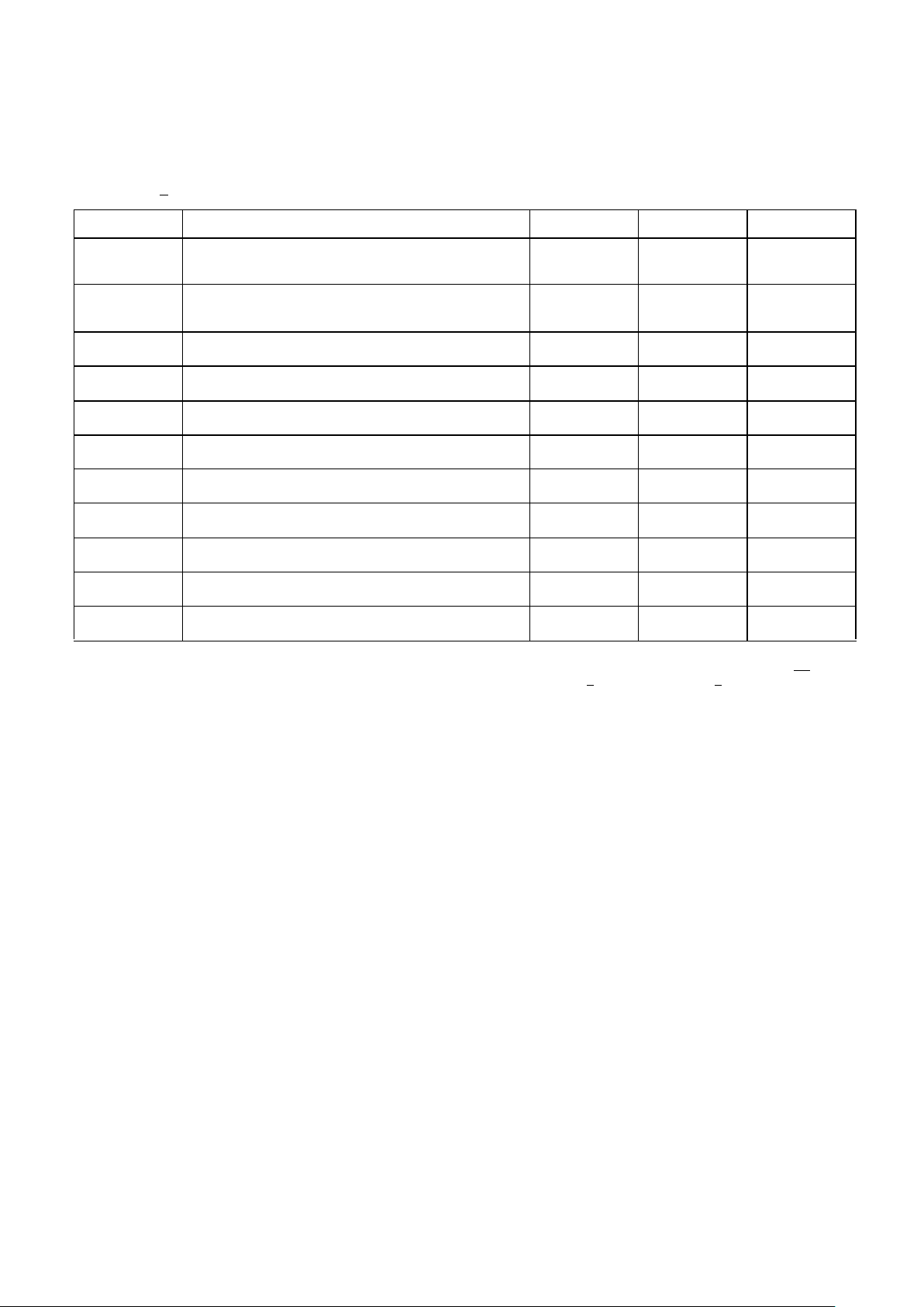
t
PHLD
6
Differential Propagation Delay High to Low
CL = 10pf (figures 4 and 5)
1.0 4.0 ns
t
PLHD
6
Differential Propagation Delay Low to High
CL = 10pf (figures 4 and 5)
1.0 4.0 ns
t
SKD
4
Differential Skew (t
PHLD
- t
PLHD
) (figures 4 and 5) 0 0.35 ns
t
SK1
4
Channel-to-Channel Skew1 (figures 4 and 5)
0 0.5 ns
t
SK2
4
Chip-to-Chip Skew5 (figures 4 and 5)
1.5 ns
t
TLH
4
Rise Time (figures 4 and 5) 1.2 ns
t
THL
4
Fall Time (figures 4 and 5) 1.2 ns
t
PHZ
4
Disable Time High to Z (figures 6 and 7) 12 ns
t
PLZ
4
Disable Time Low to Z (figures 6 and 7) 12 ns
t
PZH
4
Enable Time Z to High (figures 6 and 7) 12 ns
t
PZL
4
Enable Time Z to Low (figures 6 and 7) 12 ns
7
I
N DE
VELOPMENT
R
R
IN+
R
OUT
Receiver Enabled
Generator
50Ω
Figure 4. Receiver Propagation Delay and Transition Time Test Circuit or Equivalent Circuit
R
IN-
50Ω
10pF
R
IN-
R
IN+
R
OUT
t
PHLD
V
OL
V
OH
+1.1V
50%
+1.2V
t
THL
20%
80%
50%
20%
80%
t
TLH
0V Differential
Figure 5. Receiver Propagation Delay and Transition Time Waveforms
t
PLHD
VID = 200mV
+1.3V

I
N
D
EVE
L
OP
M
E
NT
8
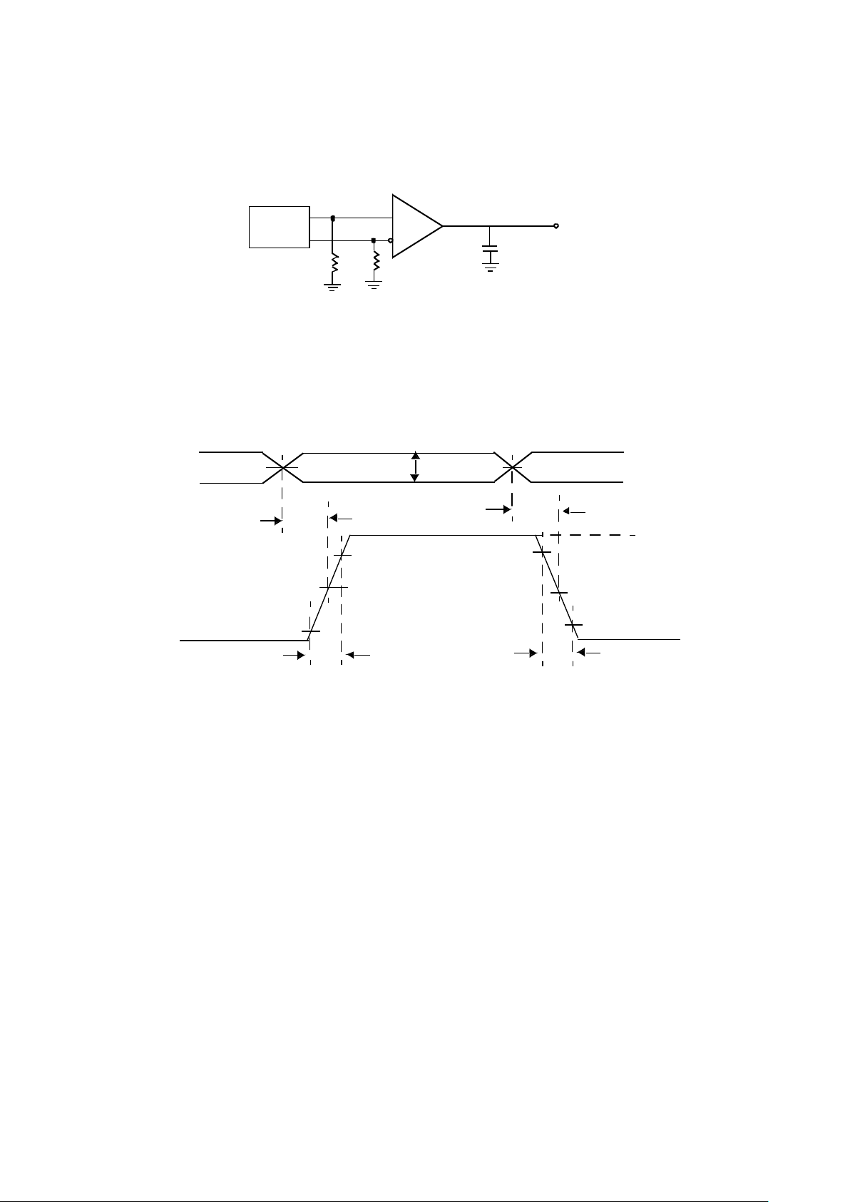
Figure 6. Receiver Three-State Delay Test Circuit or Equivalent Circuit
R
IN+
R
IN-
EN V
DD
2K
2K
10pf
EN when EN = V
DD
EN when EN = V
SS
Output when
VID = -100mV
Output when
VID = +100mV
t
PHZ
t
PZH
0.5V
50%
V
OH
V
OZ
V
OZ
0V
V
DD
0V
V
DD
1.5V
1.5V
1.5V
1.5V
0.5V
t
PZL
t
PLZ
Figure 7. Receiver Three-State Delay Waveform
50%
V
OL

9
I
N DE
VELOPMENT
Notes:
1. All exposed metalized areas are gold plated over electroplated nickel per MIL-PRF-38535.
2. The lid is electrically connected to VSS.
3. Lead finishes are in accordance to MIL-PRF-38535.
4. Package dimensions and symbols are similar to MIL-STD-1835 variation F-5A.
5. Lead position and coplanarity are not measured.
6. ID mark symbol is vendor option.
7. With solder, increase maximum by 0.003.
Figure 8. 16-pin Ceramic Flatpack
PACKAGING

I
N
D
EVE
L
OP
M
E
NT
10
ORDERING INFORMATION
UT54LVDS032LVT QUAD RECEIVER:
UT 54LVDS032LV- * * * * *
Device Type:
UT54 LVDS032LVT L VDS
Access Time:
Not applicable
Package Type:
(U) = 16-lead Flatpack (dual-in-line)
Screening:
(C) = Military Temperature Range flow
(P) = Prototype flow
Lead Finish:
(A) = Hot solder dipped
(C) = Gold
(X) = Factory option (gold or solder)
Notes:
1. Lead finish (A,C, or X) must be specified.
2. If an “X” is specified when ordering, then the part marking will match the lead finish and will be either “A” (solder) or “C” (gold).
3. Prototype flow per UTMC Manufacturing Flows Document. Tested at 25°C only. Lead finish is GOLD ONLY. Radiation neither
tested nor guaranteed.
4. Military Temperature Range flow per UTMC Manufacturing Flows Document. Devices are tested at -55°C, room temp, and 125°C.
Radiation neither tested nor guaranteed.
11
I
N DE
VELOPMENT
UT54LVDS032LVT QUAD RECEIVER: SMD
5962 -
* * *
Federal Stock Class Designator: No Options
Total Dose
(R) = 1E5 rad(Si)
(F) = 3E5 rad(Si)
(G) = 5E5 rad(Si)
(H) = 1E6 rad(Si)
Drawing Number: TBD
Device Type
01 = LVDS Receiver, 300k, 500k and 1M Rad(Si)
02 = LVDS Receiver, 100k Rad(Si)
Class Designator:
(Q) = QML Class Q
(V) = QML Class V
Case Outline:
(Y) = 16 lead Flatpack (dual-in-line)
Lead Finish:
(A) = Hot solder dipped
(C) = Gold
(X) = Factory Option (gold or solder)
**
TBD
Notes:
1.Lead finish (A,C, or X) must be specified.
2.If an “X” is specified when ordering, part marking will match the lead finish and will be either “A” (solder) or “C” (gold).
3.Total dose radiation must be specified when ordering. QML Q and QML V not available without radiation hardening.
 Loading...