

UTMC 5962R9855202VZC, 5962R9855202VYC, 5962R9855202VXX, 5962R9855202VXC, 5962R9855202VXA Datasheet
...
Standard Products
UT69R000 RadHard MicroController
Data Sheet
July 2002
q Harvard architecture
- 64K data space
- 1M instruction space
q High throughput engine
- 2 clocks per instruction
- 8 MIPS @ 16 MHz
- Static design
q 15 levels of interrupts
- 8 external user defined interrupts
- Machine error and power fail
q Two on-board 16-bit interval timers
- Timer A, 10 µs/bit
- Timer B, 100 µs/bit resolution
q 8-bit software controlled output discrete bus
q Register- oriented architecture has 21
user-accessible registers
- 16-bit or 32-bit register configurations
q Supports direct memory access (DMA) system
configuration
q Built-in 9600 baud UART
q Full military operating temperature range, -55oC to
+125oC, in accordance with MIL-PRF-38535 for Class Q
or V
q Typical radiation performance:
- Total dose: 1.0E6 rads(Si)
- SEL Immune >100 MeV-cm2/mg
- LETTH(0.25) = 60 MeV-cm2/mg
- Saturated Cross Section (cm2) per bit, 1.2E-7
- 2.3E-11 errors/bit-day, Adams to 90%
geosynchronous heavy ion
q Post-radiation AC/DC performance characteristics
guaranteed by MIL-STD-883 Method 1019 testing
at 1.0E6 rads(Si)
q Latchup immune 1.5-micron CMOS, epitaxial,
double-level-metal technology
q Packaging options:
- 132-lead flatpack
- 144-pin pingrid array (plus one index pin)
32
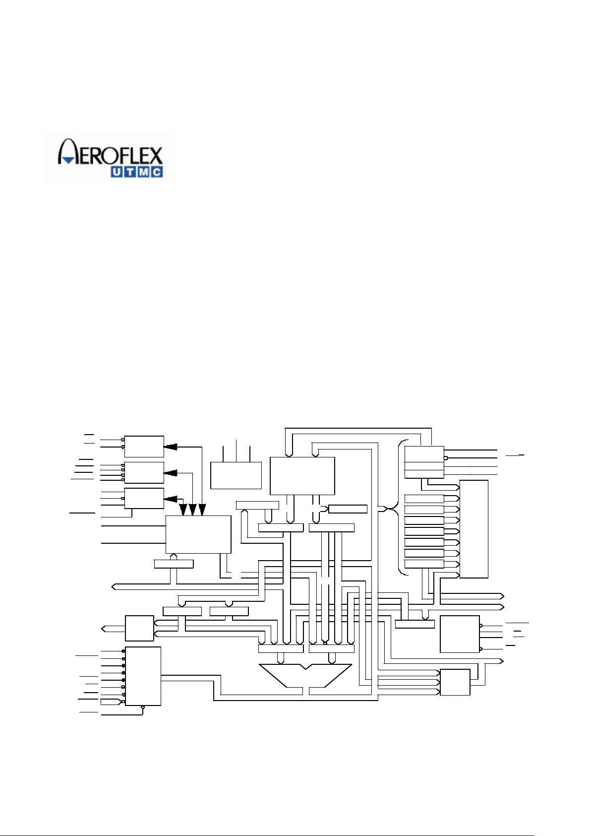
Figure 1. UT69R000 Functional Block Diagram
OE
WE
BRQ
BGNT
BUSY
BGACK
NUI1
NUI2
NUI3
STATE1
DI1
DI2
INSTRUCTION
DATA
INSTRUCTION
ADDRESS
MCHNE1
BTERR
MCHNE2
MPROT
PFAIL
INT5
INT6
INT0-4
MRST
20
16
32
32
32
ADD
MUX
MEMORY
CONTROL
BUS
ARBITRA-
TION
PROCES-
SOR
STATUS
PROCESSOR
CONTROL
LOGIC
OSCILLATOR
/CLOCK
GENERAL
PURPOSE
REGISTERS
OSCIN
OSCOUT
SYSCLK
ID
IC/ICs ACC
SHIFT REG
TEMP DEST
32
32
TEMP SRC
BIT REG
32
32
A MUX B MUX
32-BIT ALU
16
32
16
16
ADDR
MUX
BUS
CONTROL
UART
TBR
RBR
TIMCLK
TEST
UARTOUT
UARTIN
TR
TB
IM
FR
PI
ST
SW
16
16
16
16
5
16
8
OD(7:0)
OPERAND
DATA
DTACK
M/IO
R/ WR
DS
OPERAND
ADDRESS
PIPELINE
I/O
MUX
INTERRUPTS
16
16
16
16

2
Table of Contents
1.0 Introduction.....................................................................................................................4
1.1 General Description ..............................................................................................4
1.2 General Operation.................................................................................................4
2.0 Register File .................................................................................................................... 6
2.1 General Purpose Registers ....................................................................................6
2.2 Specialized Registers ............................................................................................6
2.2.1 Specialized Register Description.................................................................6
3.0 Instruction Port..............................................................................................................16
3.1 Instruction Port Operations.................................................................................17
3.1.1 STRI Instruction Bus Cycle .......................................................................17
3.1.2 LRI Instruction Bus Cycle.........................................................................18
4.0 Operand Port ................................................................................................................. 19
4.1 Operand Bus Cycle Operation ............................................................................20
4.2 DMA Operation and Bus Arbitration..................................................................23
5.0 Discrete Input/Output....................................................................................................25
5.1 Output Discrete Bus............................................................................................25
5.2 Discrete Inputs .................................................................................................... 26
6.0 Interrupts ....................................................................................................................... 26
6.1 Interrupt Control .................................................................................................26
6.1.1 Interrupt Status........................................................................................... 27
6.1.2 Interrupt Processing and Vectoring ...........................................................27
6.2 Interrupt Sources.................................................................................................28
6.3 Interrupt Hardware..............................................................................................28
6.4 Interrupt Latency.................................................................................................28
7.0 Monitor .........................................................................................................................28
7.1 Using the Monitor...............................................................................................29
7.1.1 Examine Command.................................................................................... 33
7.1.2 Modify Command ...................................................................................... 33
7.1.3 Continue Command...................................................................................34
7.1.4 Run Command...........................................................................................34
8.0 Internal UART Operation .............................................................................................34
8.1 UART Transmitter Operation.............................................................................34
8.2 UART Receiver Operation..................................................................................35
9.0 Programming Interface..................................................................................................35
9.1 Data Formats.......................................................................................................35
9.2 Instruction Formats .............................................................................................36
9.3 Addressing Modes...............................................................................................37
9.4 Data Movement Operations ................................................................................38
10.0 Pin Description..............................................................................................................39
11.0 Absolute Maximum....................................................................................................... 46
12.0 Recommended Operating Conditions ........................................................................... 46
13.0 DC Electrical Characteristics ........................................................................................47
14.0 AC Electrical Characteristics ........................................................................................48
15.0 Packaging ...................................................................................................................... 58
16.0 Ordering ........................................................................................................................60
3
DS
R/
M/
DTACK
BGACK
BUSY
BGNT
BRQ
MCHNE1
WE
OE
MRST
INT6
INT5
PFAIL
INT0
INT1
INT2
INT3
INT4
NUI4
TEST
EXCEPTIONS
INTERRUPTS/
INSTRUCTION DATA PORT
OSCIN
OSCOUT
UARTIN
UARTOUT
TIMCLK
UT69R000
RA19
RA18
RA17
RA16
RA15
RA14
RA13
RA12
RA11
RA10
RA9
RA8
RA7
RA6
RA5
RA4
RA3
RA2
RA1
RA0
NUI1
NUI3
BTERR
MCHNE2
MPROT
A0
A1
A2
A3
A4
A5
A6
A7
A8
A9
A10
A11
A12
A13
A14
A15
OD7
OD6
OD5
OD4
OD3
OD2
OD1
SYSCLK
INSTRUCTION
ADDRESS
BUS
PROCESSOR
STATUS
OSCILLATOR
UART
DATA BUS
MEMORY
ADDRESS
BUS
CLOCK
OUTPUT
BUS
CONTROL
BUS
ARBITRATION
OD0
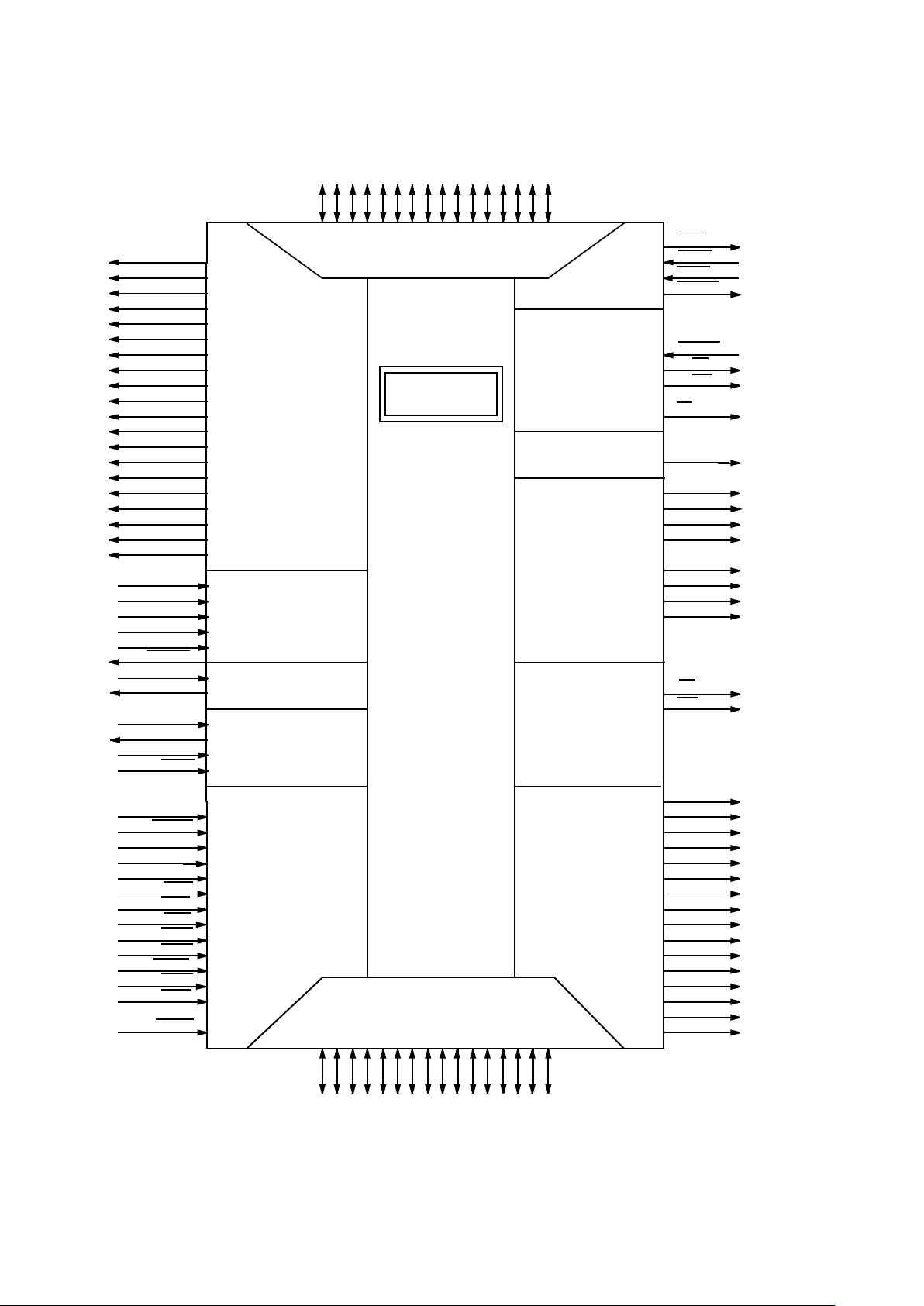
Figure 2. UT69R000 Pin Function Diagram
DI1
DI2
STATE1
RD0 - RD15
D0 - D15
OPERAND
OPERAND
NUI2
DISCRETES
WR
IO
4
1.0 Introduction
The UT69R000 is a radiation-hardened high-performance
microcontroller designed, manufactured, and tested to meet
rigorous radiation environments. UTMC designed and
implemented the UT69R000 using an advanced radiationhardened twin-well CMOS process. The combination of
radiation-hardness, high throughput, and low power
consumption makes the UT69R000 ideal for high-speed
systems in satellites, missiles, and avionics applications.
1.1 General Description
The UT69R000 is a versatile microcontroller designed to meet
real-time control type applications. Support functions often
found external to a microprocessor are integrated within the
microcontroller. Functions include UART, interval timers, 10
external interrupt vectors, and a 8-bit output discrete bus.
The UT69R000 core (machine) is a two port microcontroller
that accesses instructions from a 1M x 16 instruction port; a
second port (64K x 16 data port) is available for data storage.
Data transfer acknowledge allows the addition of wait states
on the data port. The machine performs overlapping fetches
and executes speeding instruction throughput. A 12 MHz
operating clock frequency provides up to 6 MIPS of
throughput. A later section of this data sheet expands on this
concept.
The UT69R000 architecture is based on 20 16-bit general
purpose registers providing, the programmer with extensive
register support. The UT69R000’s flexibility is enhanced by
the concatenation of 16-bit registers into 32-bit registers. In
addition, all registers are available for use as either the source
or destination for any register operation.
All UT69R000 circuitry is of static design. Internal registers,
counters, and latches do not require refresh as with dynamic
circuit design. Therefore the UT69R000 can operate from DC
to the upper frequency limit of 16 MHz. This type of operation
is especially useful in power critical applications such as
satellites.
The UT69R000 fully supports multiprocessor systems, DMA,
and complex bus arbitration. Bus control passes among bus
masters operating on the same bus. The bus master can be one
of several UT69R000s or any other device requiring DMA.
The UT69R000 supports 15 levels of vectored interrupts. Ten
of these are external interrupts, all of which are user-definable.
All interrupts are serviced in order of priority.
The UT69R000’s three basic instruction formats support 16bit and 32-bit instruction. The formats are Register-to-Register,
Register-to-Literal, and Register-to-Long-Immediate
instructions.
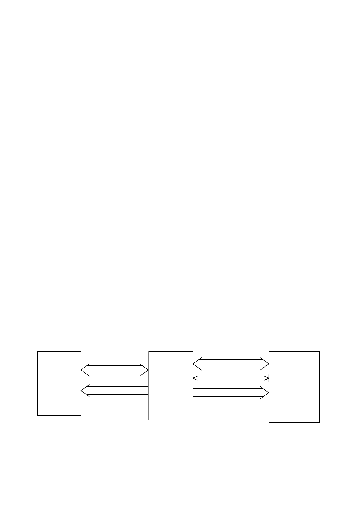
Figure 3 shows the UT69R000’s general system architecture.
1.2 General Operation
The UT69R000 reduced instruction set consists of 35 separate
instructions. Most of these instructions execute in two clock
cycles providing high-throughput. The UT69R000 has a
Harvard architecture which incorporates two address and two
data buses. One set of address and data buses interface with
instruction memory (instruction port) and the other interfaces
with data memory (data port). The instruction port consists of
a 20-bit address bus and 16-bit data bus. The maximum
program length of any program is 1 mega-word. The data port
consists of a 16-bit address and data bus, allowing access to
64K x 16 of data storage.
The instruction port is dedicated to the storage of instruction
code; however , two instructions exist that allow the instruction
port manipulation by the machine. These instructions are the
Load Register from Instruction Memory (LRI) and Store
Register to Instruction Memory (STRI).
16
20
16
16
ADDRESS
Figure 3. UT69R000 General System Architecture
CONTROL
DATA
MEMORY
INSTRUCTION
INSTRUCTION
INSTRUCTION
UT69R000
DATA
MEMORY
DATA
ADDRESS
5
The UT69R000 begins operation by first generating an address
on the instruction port; valid data (instruction) is then latched
into the Primary Instruction Register (PIR). After the machine
stores the instruction in the PIR, the machine begins execution
of the instruction in the Instruction Register (IR). If the present
instruction in the IR requires only internal processing, the
machine does not exercise the data bus. If the machine needs
additional data to complete the instruction the machine begins
arbitration for the data port.
Data port arbitration begins with the machine asserting the Bus
Request (BRQ) signal. The machine samples the Bus Grant
(BGNT) and Bus Busy (BUSY) signals on the falling edge of
the clock (OSCIN). When the machine detects that the previous
bus controller has relinquished control of the bus, the machine
generates a Bus Grant Acknowledge (BGACK) signal
signifying that it has taken control of the bus (i.e., data port).
After the UT69R000 takes control of the bus, it generates valid
address and data information. If the machine is interfacing to
slow memory or other peripheral devices that require long
memory-access times, the Data Transfer Acknowledge
(DTACK) signal extends the memory cycle time. By holding
off the assertion of DTACK, the slow device lengthens the
memory cycle until it can provide data for the machine.
The UT69R000 controls the vectoring and prioritizing of
interrupt service. Internal logic selects one of 15 interrupt
vectors, each interrupt vector is allocated four memory
locations. Use the four memory locations to store return from
interrupt service address information along with the interrupt
service routine’s location. The UT69R000 controls prioritizing
of coincident interrupts.
Perform UART control and maintenance via input/output
commands OTR and INR. These commands allow the
programmer to read UART status, and error information, as
well as upload and download information to the receive and
transmit buffers respectively.
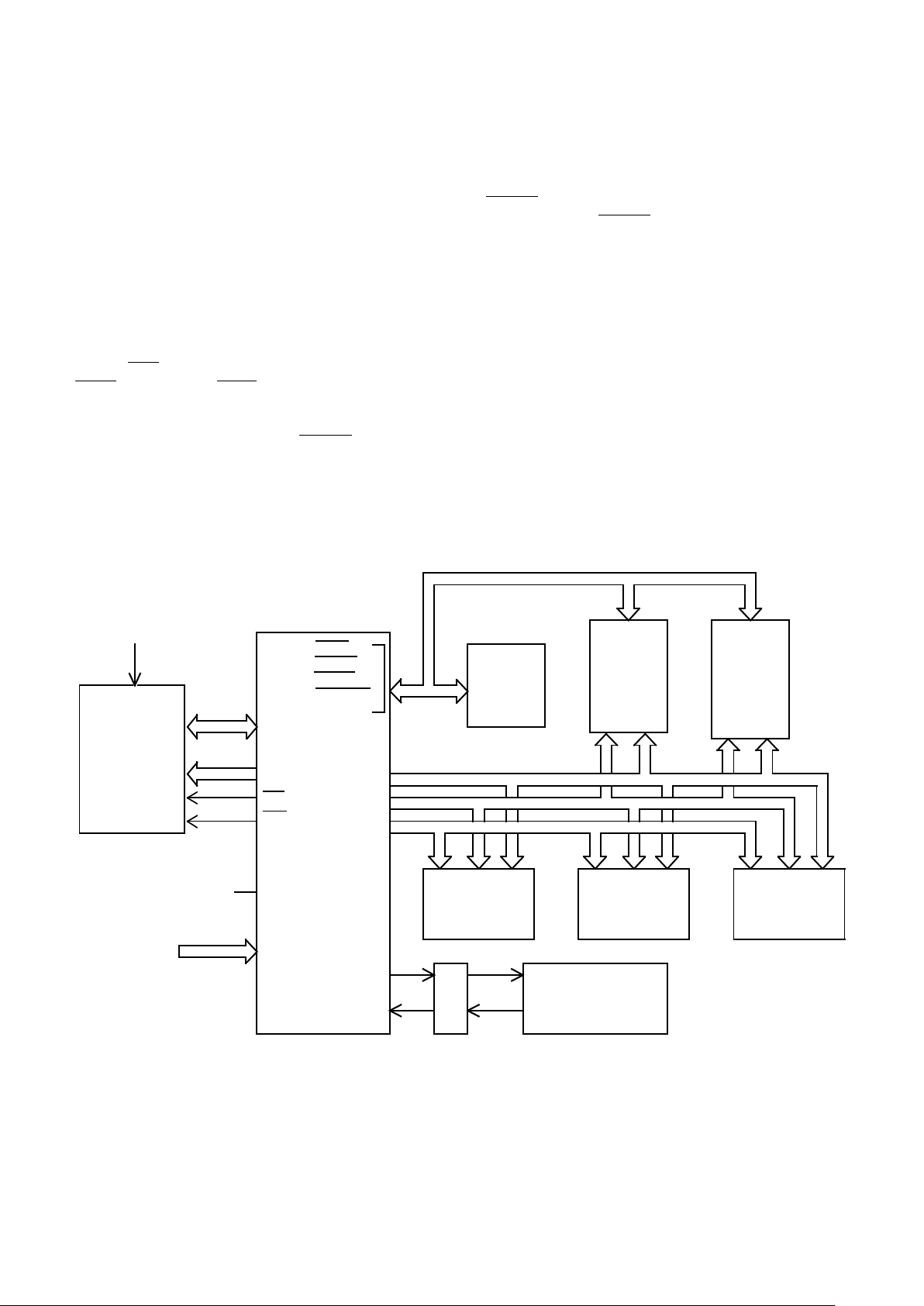
Figure 4 shows an example of a system configuration.
INSTRUCTION
DATA
INSTRUCTION
ADD
16
20
NUI3
USERDEFINED
SYSTEM
INTERRUPTS
8
UART
I/F
X
C
V
R
GENERAL
PURPOSE
MEMORY
I/O
DEVICE #1
I/O
DEVICE #2
BUS
ARBITER
DMA
DEVICE
#1
1553
I/F
DMA
DEVICE
#2
OP ADD
OP DATA
CONTROL
16
16
6
Figure 4. The UT69R000 Example System Configuration
4
UT69R000
INSTRUCTION MEMORY
CAN ONLY BE ACCESSED
BY THE UT69R000
INSTRUCTION
MEMORY
1M X 16
INTERNALLY
PULLED LOW
SERIAL I/O
BUSY
BGACK
BRQ
BGNT
OE
WE
(MAX)
6
2.0 Register File
The UT69R000 has a register-oriented architecture. The
registers within the machine fall into two categories, general
purpose and specialized registers. All registers are accessible
to the programmer through the instruction set. The programmer
uses data from these registers to perform arithmetic and logical
functions, alter program flow, detect various system and
machine faults, determine machine status, control UART and
timer functions, and for exception handling.
2.1 General Purpose Registers
Figure 5 shows the UT69R000’s 20 general purpose registers.
The UT69R000 normally accesses these registers as singleword 16-bit registers although the machine can concatenate
these registers into 32-bit double-word register pairs. When the
programmer uses the general purpose registers as a doubleword register pair, the most significant 16 bits of the 32-bit
words are stored in the even-numbered register of the register
pair. For instance, if a 32-bit word is stored in Register Pair
XR6, the most significant word is stored in register R6 and the
least significant word is stored in register R7.
In addition to the 20 general purpose registers, the UT69R000
has a 32-bit accumulator (ACC). The ACC is normally a
destination register, although under certain circumstances it
can be the source register (INR RD, ACC). The accumulator
retains the most significant half of the product during a multiply
instruction or the remainder during a divide operation.
2.2 Specialized Registers
The UT69R000 has 13 special purpose registers. These
registers control machine configuration, report status, and
interrupts. Below is a list of the special purpose registers. The
values in the brackets indicate the power-up condition.
1. Stack Pointer Register (SP) [XXXX (hex)]
2. System Status Register (STATUS) [XXXX (hex)]
3. UART Receiver Buffer Register (RCVR)
[XX00 (hex)]
4. UART Transmitter Buffer Register (TXMT)
[XX00 (hex)]
5. Pending Interrupt Register (PI) [0000 (hex)]
6. Fault Register (FT) [0000 (hex)]
7. Interrupt Mask Register (MK) [XXXX (hex)]
8. Status/Output Discrete Register (SW)
[XXFF (hex)]
9. Instruction Counter Register (IC) [0000 (hex)]
10. Instruction Counter Save Register (ICS)
[XXXXX (hex)]
11. Instruction Register (IR) [0000 (hex)]
12. Timer A (TA) [0000 (hex)]
13. Timer B (TB) [0000 (hex)]
The instruction set provides access to most of the special
purpose registers.
2.2.1 Register Description
Stack Pointer Register
The UT69R000 uses the 16-bit Stack Pointer Register as an
address pointer on PUSH and POP instructions. The machine
pre-increments (POP) and post-decrements (PUSH) the Stack
Pointer contents. The programmer loads and stores the SP by
executing the INR and OTR commands to the stack pointer.
Bit 15 is the most significant bit, the least significant bit is bit
zero.
System Status Register
The System Status Register provides status information on the
UT69R000’s internal operation, including status of the internal
UART. The register is read via the INR Rd, STATUS
instruction. Bit definitions follow.
Figure 5. General Register Set
CONCATENATED 32-BIT
ACC
XR18
XR16
XR14
XR12
XR10
XR8
XR6
XR4
XR2
XR0
R19
R17
R15
R13
R11
R9
R7
R5
R3
R1
ACCUMULATOR
R6
R18
R16
R14
R12
R10
R8
R4
R2
R0
REGISTER PAIR
16 BITS16 BITS
15 141312111098754321
0
C P Z N V J
I
M
M
E
6
O
E
R
E
FEPEC
N
T
B
E
TED
R
MSB LSB
Figure 6. The System Status Register (STATUS)
E

7
Bit Number Mnemonic Description
Bit 15 C Carry. This conditional status is set if a carry is generated
or no borrow. [0]
Carry Equations:
C= (Dm * Sm * Rm) + (Dm * Sm * Rm)
+(Dm * Sm * Rm)
Where: Dm destination register most significant bit
Sm - source register most significant bit
Rm - result most significant bit (stored in
destination register)
Bit 14 P Positive. This conditional status is set if the result of an
operation is positive. [0]
Positive Equation: P = N * Z
Bit 13 Z Zero. This conditional status is set if the result of an
operation is negative. [0]
Zero Equation:Z = Rm * Rm-1 * Rm-2 * R0
Bit 12 N Negative. This conditional status is set if the result of an
operation is negative. [0]
Negative Equation: N = Rm
Bit 11 V Overflow. This conditional status is set if the result when an
overflow condition occurs. [0]
Overflow Equation:
V = (Dm * Sm * Rm) + (Dm * Sm * Rm)
Bit 10 J Normalized. This conditional status is set as the result of a
long instruction and the result is normalized. [0]
Normalized Equation: J = (R32 XOR R31)
Bit 9 IE Interrupts Enabled. This bit reflects whether interrupts are
disabled or enabled. OTR Rd, ENBL and OTR Rd, DSBL
control this bit and function. [0]
Bit 8 MME Discrete Input 1. This bit reflects the input stimulus applied
to the input pin.
Bit 7 RE Receiver Error. This bit is the logical OR combination of the
OE, FE, and PE status bits. [0]
Bit 6 OE Overrun Error. When active, this bit indicates that at least
one data word was lost because the Data Ready (DR bit 0 of
the Status Register) signal was active twice consecutively
without an INR Rd, RCVR. [0]
8
UART Receiver Register (RCVR)
The UART Receiver Buffer Register (see figure 7) receives
9600-baud asynchronous serial data through the UARTIN
input pin on the UT69R000. Each serial data string contains an
active-low Start bit, eight Data bits, an odd Parity bit, and an
active-high Stop bit. Figure 8 shows a single serial data string.
While receiving a serial data string, the UT69R000 generates
four status flags: Data Ready (DR), Overrun Error (OE),
Framing Error (FE), and Parity Error (PE). The UT69R000
stores these bits in the System Status Register.
Receiver buffer register bits 15-8 are always low. Bit numbers,
7 to 0 (RCD7 - RCD0) contain data the UT69R000 receives
via the serial data port. RCD7 is the MSB; RCD0 is the LSB.
Bit 5 FE Framing Error. When active, this bit indicates a stop bit was
missing from the serial transmission string. Cleared on next
transmission. [0]
Bit 4 PE Parity Error. When active, this bit indicates the serial
transmission was received with the incorrect parity. Cleared
on next transmission. [0]
Bit 3 CN Discrete Input 2. This bit reflects the input stimulus applied
to the input pin.
Bit 2 TBE UART Transmitter Buffer Empty. This bit indicates the
Transmitter Buffer Register is empty and ready for data. [0]
Bit 1 TE UART Transmitter Empty. This bit is low while the UART
is transmitting data and goes high when the transmission is
complete. [0]
Bit 0 DR UART Data Ready. This active-high signal indicates the
UART received a serial data word and this data is available.
Cleared on the execution of INR Rd, RCVR. [0]
Bit Number Mnemonic Description
15 14 13 12 11 10 9 8 7 5 4 3 2 1 0
0 50 40 30 20 10 070 60
6
R
C
D
R
C
D
R
C
D
R
C
D
R
C
D
R
C
D
R
C
D
R
C
D
MSB LSB
Figure 7. The UART Receiver
Buffer Register (RCVR)
54T 3
R
20 1
S
T
D
7
R
C
D
R
C
D
R
C
6
R
C
D
R
C
D
R
C
D
R
C
D
R
CDP
A
S
T
O
Figure 8. UART Receiver Single
Serial Data String
PR
DATA
FLOW
9
UART Transmitter Buffer Register
The UT69R000’s internal UART forms an 11-bit serial string
by combining a Start bit, the eight Data bits from the
Transmitter Buffer Register, an odd Parity bit, and a Stop bit.
Figure 9 shows the composition of the serial data string. The
UT69R000 transmits this serial string through the UARTOUT
pin at a rate of 9600 baud (TIMCLK = 12MHz).
The UT69R000’s internal UART has a double-buffered data
transmission register (figure 10). The UT69R000 first loads
the data for transmission into the Transmitter Buffer Register.
If the UART Transmitter Register is empty, data from the
Transmit Buffer Register automatically transfers to the UART
Transmitter Register. At this time, the TBE bit goes active
indicating more data may be loaded into the Transmit Buffer
Register. This double-buffering scheme allows contiguous
transmission of serial data streams and also decreases the
UT69R000’s required overhead for the UART interface. The
UT69R000 loads the 8-bit Transmit Buffer Register via the
OTR Rd, TXMT instruction.
Two status signals are associated with transmitting serial data.
These signals are the UART Transmitter Buffer Empty (TBE)
and UART Transmitter Register Empty (TE). TBE and TE are
both active high and provide information on the status of double
buffering the UART’s transmitted data. TBE and TE are read
from the System Status Register bits 2 and 1
respectively.
54T 3
R
20 1
S
T
D
7
T
X
D
T
X
D
T
X
6
T
X
D
T
X
D
T
X
D
T
X
D
T
XDP
A
S
T
O
Figure 9. UART Transmitter Data String
PR
DIRECTION
OF DATA
FLOW OUT
OF THE
UT69R000
Figure 10. The UT69R000 UART Double-Buffered Transmitter Register
REGISTER (OTR) INSTRUCTION
TBR WITH AN OUTPUT
DATA IS LOADED INTO THE
OF THE SYSTEM STATUS
READ FROM BIT 1
TRANSMITTER REGISTER IS
STATUS OF THE UART
8
REGISTER
UART TRANSMITTER
REGISTER (TBR)
UART TRANSMITTER BUFFER
16
DATA BUS
THE UT69R000’s INTERNAL
FROM BIT 2
TBR IS READ
STATUS OF THE
DATA FLOW
DIRECTION OF
T
R
T
S
01234567
X
T
X
T
X
T
X
T
X
T
X
T
X
T
X
T
R
A
P
P
O
T
S
0123456
D
X
T
D
X
T
D
X
T
D
X
T
D
X
T
D
X
T
D
X
T
7
D
X
T
D
C
D
C
D
C
D
C
D
C
D
C
D
C
D
C
OF THE SYSTEM
REGISTER
STATUS REGISTER

10
Pending Interrupt Register
The Pending Interrupt Register (PI) contains information on
pending interrupts attempting to vector the Instruction Counter
Register to a new location. Software or hardware controls the
Pending Interrupt Register contents. Any system interrupt,
when active, sets the corresponding bit in the register. OTR
and INR instruction can also set, clear, and read the Pending
Interrupt Register (figure 11).
Instruction INR Rd, PI stores the PI contents in the destination
register. OTR Rd, PI loads the PI with the contents of the
destination register. OTR Rd, RPI clears the PI register. For
each bit set, to a logic one, in the destination register the
corresponding PI bit is cleared. To clear the PI, first read the
PI, then clear only the bits set to a logic one. Reading, then
clearing the PI prevents the inadvertent clearing of interrupts
occurring during execution of an OTR Rd, RPI command.
Example:
CLEAR: INR Rd, PI
OTR Rd, RPI
To generate a software interrupt clear the corresponding bit in
the PI register before writing to the PI register.
Example:
WRITE: MOV R1, 1000 (hex)
OTR R1, RPI
OTR R1, PI
Note: Do not enable interrupts while the PI is non-zero.
Bit Number Mnemonic Description
Bit 15 PWDN Power Fail
Bit 14 MCHE Machine Error Interrupt
Bit 13 INT0 External Interrupt 0
Bit 12 USR3 Software Interrupt 3
Bit 11 FIPO Fix Point Overflow
Bit 10 USR2 Software Interrupt 2
Bit 9 USR1 Software Interrupt 1
Bit 8 TIMA Timer A Interrupt
Bit 7 INT1 External Interrupt 1
Bit 6 TIMB Timer B Interrupt
Bit 5 INT2 External Interrupt 2
15 14 13 12 11 10 9 8 7 5 4 3 2 1 0
P
W
D
N
M
C
H
E
I
N
T
O
U
S
R
3
F
I
P
O
U
S
R
2
U
S
R
T
I
M
6
T
I
M
I
N
T
I
N
T
I
N
T
I
N
T
I
N
T
I
N
T
N
/
U
MSB LSB
Figure 11. The Pending Interrupt Register (PI)
1 A 1 B 2 3 6 4 7

11
Bit 4 INT3 External Interrupt 3
Bit 3 INT6 External Interrupt 6
Bit 2 INT4 External Interrupt 4
Bit 1 INT7 External Interrupt 7
Bit 0 NU Not Used*
*Note:
The UT69R000 interrupt control hardware is designed such that the following sequence always occurs:
The machine will vector to the lowest priority interrupt (vector 43Chex) if interrupts are disabled after an interrupt is latched into
the PI register. Interrupts are latched into the PI register on the falling edge of STATE1, interrupts are disabled on the falling edge
of clock CK1 internal (rising edge of CK2). The UT69R000 vectors to address 43C (hex) during the fetch cycle of the command
following the disable command.
Work Around: Vector 43C hex is not used as a normal interrupt; instead it is used to store the interrupt that occurred coincident
with disabling of interrupts. The coincident interrupt is serviced after the interrupts are re-enabled by software.
43C: INR RD, ICS
JC x, PSEUDO
NOP
PSEUDO: INR RD, PI ; read PI
OTR RD, RPI :clear PI
OTR RD, PI ;reset PI register, saves coincident interrupt
CALL RD, RD ;return
The interrupt service routine saves the interrupt that was coincident with the disable interrupt instruction. The UT69R000 will vector
to that interrupt after interrupts are re-enabled. The interrupt service routine (@43C) does not affect the condition code flags.

12
Fault Register
The UT69R000 uses the Fault Register (FT) to indicate the
occurrence of a machine-error fault. A machine-error fault
cannot be disabled. The UT69R000 uses the logical OR
combination of the 16 bit FT to generate a Machine Error
interrupt, bit 14 of the PI. Any bits in the FT the UT69R000
does not use are set to a logic zero. The UT69R000 reads,
writes, and clears the FT with INR and OTR instructions. Fault
Register bits reflecting external pins are level sensitive; bit(s)
cannot be reset until the external signal is negated.
15 141312111098754321
0
MEM PARITY I/OSY
F
6
ILLEGALTR
E
S
BUILT-
MSB LSB
Figure 12. The Fault Register (FT)
PROT
INSTRUCTION AND
ADD FAULT
IN-
TEST
Bit Number Mnemonic Description
Bit 15 CMPF CPU Memory Protect Fault. This bit indicates the UT69R000 has
detected an access fault on the operand but (i.e., attempted access
to write or read-protected memory). This bit is asserted only when
the UT69R000 is controlling the Operand Data Bus and the
MPROT input is asserted. [0]
Bit 14 DMPF DMA Memory Protect Fault. This bit indicates a DMA device has
detected an access fault (i.e., attempted access to write or readprotected memory). This bit is asserted when the UT69R000 is
not controlling the Operand Data Bus and the MPROT input is
asserted.
Bit 13 MCHNE2 Machine Error 2. This bit indicates that a user-defined machine
error has occurred. Reflects status of external input pin MCHNE2.
Bit 12 SFT8 Software Error 8. This bit indicates that a user-defined software
machine error has occurred.
Bit 11 SFT7 Software Error 7. This bit indicates that a user-defined software
machine error has occurred.
Bit 10 BTERR2 I/O Bus Timer Error. This bit indicates that a bus or time-out error
occurred. The bit is set if the UT69R000 is performing an I/O
access and BTERR input is asserted.
Bit 9 SFT6 Software Error 6. This bit indicates that a user-defined software
machine error has occurred.
Bit 8 MCHNE1 Machine Error 1. This bit indicates that a user-defined machine
error has occurred. It reflects the status of external input pin
MCHNE1.
Bit 7 BTERR1 Memory Bus Timer Error. This bit indicates that a bus or time-out
error occurred. The bit is set if the UT69R000 is performing a
memory access and the BTERR input is asserted.

13
Bit 6 SFT6 Software Error 6. This bit indicates that a user-defined software
machine error has occurred.
Bit 5 SFT5 Software Error 5. This bit indicates that a user-defined software
machine error has occurred.
Bit 4 SFT4 Software Error 4. This bit indicates that a user-defined software
machine error has occurred.
Bit 3 SFT3 Software Error 3. This bit indicates that a user-defined software
machine error has occurred.
Bit 2 SFT2 Software Error 2. This bit indicates that a user-defined software
machine error has occurred.
Bit 1 SFT1 Software Error 1. This bit indicates that a user-defined software
machine error has occurred.
Bit 0 SFT0 Software Error 0. This bit indicates that a user-defined software
machine error has occurred.
Bit Number Mnemonic Description

14
Interrupt Mask Register
The Interrupt Mask Register (MK) contains one mask bit for
each of the 15 system interrupts. All bits in the MK are set or
reset under software control, setting bits 15 and 10 has no effect
on the UT69R000’s interrupt operation because these
interrupts cannot be masked. The UT69R000 reads and writes
the MK with instructions OTR Rd,MK and INR Rd,MK. A
logical one unmasks an interrupt; logic zero masks an interrupt.
Bit Number Mnemonic Description
Bit 15 PWDN Non-Maskable Interrupt
Bit 14 MCHE Machine Error Interrupt
Bit 13 INT0 External Interrupt 0
Bit 12 FLPO Software Interrupt 3
Bit 11 FIPO Fix Point Overflow
Bit 10 EXCL Software Interrupt 2
Bit 9 FLPN Software Interrupt 1
Bit 8 TIMA Timer A Interrupt
Bit 7 INT1 External Interrupt 1
Bit 6 TIMB Timer B Interrupt
Bit 5 INT2 External Interrupt 2
Bit 4 INT3 External Interrupt 3
Bit 3 IOLI External Interrupt 6
Bit 2 I0L2 External Interrupt 4
Bit 1 INT7 External Interrupt 7
Bit 0 NU Not Used (see Note on page 11)
15 14 13 12 11 10 9 8 7 5 4 3 2 1 0
P
W
D
N
M
C
H
E
I
N
T
O
F
L
P
O
F
I
P
O
E
X
C
L
F
L
P
T
I
M
6
T
I
M
I
N
T
I
N
T
I
N
T
I
O
L
I
N
T
I
O
L
N
/
U
MSB LSB
Figure 13. The Interrupt Mask Register (MK)
U A B1 2 3 1 4 2

15
Status/Output Discrete Register
The Status/Output Discrete Register reports the C, P, Z, and N
bits of the System Status Register along with controlling the
output discrete bus (OD(7:0)). Register bits C, P, Z, and N
contain the same information as the System Status Register bits
15, 14, 13, and 12. Control of the output discrete bus is allowed
via bit 0 through 7 of this register. Use input and output
instructions INR Rd, SW and OTR Rd, SW to write and read
this register. Use this register to restore the condition codes
after interrupt service routines.
Bit Number Mnemonic Description
Bit 15 C Carry
Bit 14 P Positive
Bit 13 Z Zero
Bit 12 N Negative
Bit 11 U/D User-defined
Bit 10 U/D User-defined
Bit 9 U/D User-defined
Bit 8 U/D User-defined
Bit 7 OD7 Output Discrete 7
Bit 6 OD6 Output Discrete 6
Bit 5 OD5 Output Discrete 5
Bit 4 OD4 Output Discrete 4
Bit 3 OD3 Output Discrete 3
Bit 2 OD2 Output Discrete 2
Bit 1 OD1 Output Discrete 1
Bit 0 OD0 Output Discrete 0
15 14 13 12 11 10 9 8 7 5 4 3 2 1 0
CONDITION USER-
6
DISCRETE
MSB LSB
Figure 14. The Status/Output Discrete Registers (SW)
STATUS
(CS)
DEFINED

16
Instruction Counter and Instruction Register
The UT69R000’s instruction port interface consists of a 20-bit
instruction address and a 16-bit data bus. The Instruction
Counter (IC) supplies the 20-bit address to memory. The
instruction read from memory is then stored into the Instruction
Register (IR, 16-bits wide). The IR consists of two sets of
internal latches, a Primary Instruction Register latch (PIR, 16bits wide) and the Instruction Register latch (IRL, 16-bits
wide). These two sets of latches allow the UT69R000 to
perform overlapping memory fetch and execute cycles. This
means the UT69R000 performs a delayed branch when the flow
of the program is interrupted. A delayed branch implies that
the UT69R000 fetches and executes the instruction following
the branch condition before the UT69R000 executes the first
instruction at the branch location.
Instruction Counter Save Register
The UT69R000 uses the Instruction Counter Save Register
(ICS) when servicing interrupts and branch instructions. When
an interrupt or branch occurs, the UT69R000 saves the IC in
the ICS. Read the ICS immediately after entering the target
routine to save the return location before any other IC save
occurs. The UT69R000 reads the ICS using input instruction
INR XRd, ICS. Please note that the ICS read requires a 32-bit
wide register.
Timer A and Timer B
Timer A and B registers are 16-bit binary counters. Input/
output instructions start, halt, read, and write these counters.
Timer A resolution is 10µs per bit, Timer B has a resolution of
100µs per bit (TIMCLK at 12 MHz). Each timer generates a
time-out interrupt when the counter transitions from FFFF
(hex) to 0000 (hex). Time intervals before interrupt are defined
as the difference between the loaded value and 0000 (hex). For
example, load Timer A with the value FFFE (hex), start Timer
A; an interrupt occurs 20µs later as the timer transitions from
FFFF (hex) to 0000 (hex). The Pending Interrupt Register
reflects this time-out condition.
Modify the resolution of Timer A and B by scaling the
TIMCLK input. For example, to decrease Timer A resolution
from 10µs to 64µs per bit, TIMCLK is decreased to 1.88 MHz.
3.0 Instruction Port
Instruction port signals include a 20-bit address bus RA(19:0),
a 16-bit data bus RD(15:0), and two control signals OE and
WE. During instruction and data fetch cycles, OE is asserted
(WE negated). Write operations to the port asserts WE and
negates OE. Primarily designed for fast access of instruction
information, the instruction port does not allow for the
inclusion of wait states.
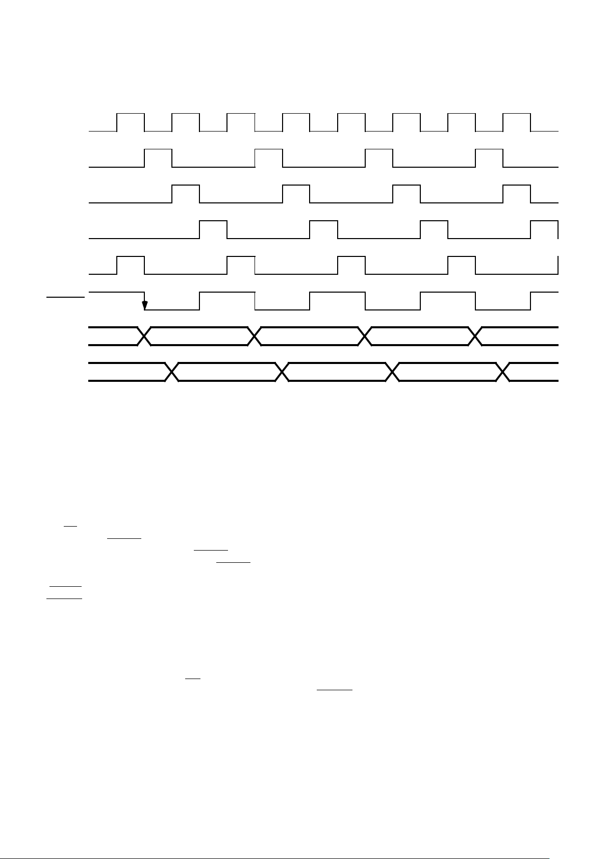
The UT69R000 divides all operations into four distinct time
periods (CK1 through CK4). These time periods are based on
the processor clock. The UT69R000 performs a separate
function during each of these four time periods.
During CK1, the UT69R000 begins executing the instruction
in the Primary Instruction Register (PIR). The instruction
executed is the instruction the UT69R000 fetched during the
previous bus cycle. Also during CK1, the instruction address
for the next instruction to fetch from memory becomes valid.
(Thus, the overlapping fetch and execute cycles of the
UT69R000.) STATE1 output goes low, indicating the
UT69R000 is executing an instruction.
The UT69R000 begins variable width clock period CK2 after
completing CK1. For 2 and 3 clock cycle instructions CK2
remains one-half clock cycle in length. During four clock cycle
instructions CK2 is stretched to one and a half clock cycles.
The following conditions extend time period CK2: (1)
Executing a STRI instruction, (2) Executing a LRI instruction,
or (3) Executing any instruction access to the operand port. The
UT69R000 also extends clock period CK2 for the Operand Port
arbitration process. The UT69R000 samples the logical AND
combination of BUSY and inverted BGNT during CK2. If this
combination is low, time period CK2 extends until the
combination of the two signals is high, indicating the
UT69R000 now controls the Operand Port. STATE1 output
remains low for the entire CK2 time period.
At the beginning of CK3, STATE1 goes high indicating the
next instruction is being fetched from memory. The
UT69R000’s operand address and data buses become active at
the beginning of CK3 along with the Bus Grant Acknowledge
(BGACK), M/IO, and R/WR signals. Data Strobe (DS) asserts
one clock cycle after the beginning of CK3, one and a half clock
cycles after the start of CK4.
Following CK3 is variable length clock period CK4. The
stretch of CK4 occurs during the following instruction
executions: (1) Executing a STRI instruction, (2) Executing a
LRI instruction, (3) Executing any instruction with Long
Immediate data (e.g., MOV Rd, FFFFh), or (4) Executing any
operand port access. After time period CK4 starts, the
transparent latches that make up the Primary Instruction
Register enable, allowing the UT69R000 to input the
instruction from memory.
17
If the instruction being executed requires access to the operand
bus, DS goes active. The UT69R000 samples the Data Transfer
Acknowledge (DTACK) on the next and every subsequent
rising edge of the processor clock. If DTACK is not low, the
UT69R000 extends time period CK4 until DTACK becomes
active or until an error condition is detected -- either Bus Error
(BTERR) or Memory Protect (MPROT) becomes active.
STATE1 remains high during the entire CK4 time period.
Figures 15, 16, and 17 show the timing relationships for CK1,
CK2, CK3, and CK4 during 2, 3, and 4 clock cycle instructions.
3.1 Instruction Port Operations
Most applications dedicate the instruction port to program
information. For these applications WE is always negated. The
UT69R000 can manipulate the instruction port through
instructions Store Register to Instruction Memory (STRI, write
access) and Load Register from Instruction Memory (LRI, read
access). Section 3.1.1 and 3.1.2 review the STRI and LRI
instructions.
3.1.1 STRI Instruction Bus Cycle
During an STRI instruction, instruction data moves from the
UT69R000 to the instruction memory. Figure 18 shows the
timing diagram of the signal relationships for the UT69R000
during STRI Instruction Bus Cycle Operation. Before the
UT69R00 executes the STRI instruction, the system
programmer must load the Accumulator Register with the
address which will receive the data. When the ACC is loaded
with the address information, the UT69R000 can begin
executing the STRI instruction.
Executing the STRI instruction begins when the falling edge
of OSCIN signals the start of time period CK1. At the beginning
of CK1, the data previously stored in the ACC becomes a valid
address on the instruction port address bus (RA(19:0)) and
STATE1 output becomes active, indicating the UT69R000 is
executing an instruction.
OSCIN
CK1
CK2
CK3
STATE1
EXECUTE FETCH
Figure 15. Machine Cycle 1 (2 Clock Cycle Instructions)
CK4
RA(19:0)
RD(15:0)
Valid Address Valid Address Valid Address
Instruction Data Instruction Data Instruction Data
18
3.1.2 LRI Instruction Bus Cycle
During an LRI instruction, the UT69R000 moves the
instruction data from the instruction memory to the
UT69R000.Figure 19 shows the timing diagram of the signal
relationships for the UT69R000 during an LRI Instruction Bus
Cycle.
Just as with the STRI instruction, before the UT69R000
executes the LRI instruction the system programmer must load
the UT69R000’s accumulator with the address from which the
data will be read. After the ACC is loaded with the address
information, LRI instruction execution can take place.
OSCIN
CK1
CK2
CK3
CK4
Figure 16. Machine Cycle 2 (3 Clock Cycle Instructions)
STATE1
EXECUTE FETCH
RA(19:0)
RD(15:0)
Note:
1. Examples of three clock cycle instructions include (operand port accesses):
LR Rd, Rs
STR Rd, Rs
STATUS
DS
A(15:0)
D(15:0)
Address Valid
Data Read
Control Valid
Fetch Address Valid
Fetch Instruction
Fetch Address Valid
Fetch Instruction
(M/IO, R/WR)
19
Executing the LRI instruction begins when the falling edge of
OSCIN signals the start of time period CK1. At the beginning
of CK1, the data previously stored in the ACC becomes a valid
address on the instruction port address bus (RA(19:0)) and
STATE1 output becomes active indicating the UT69R000 is
executing an instruction.
The data on the data bus is read into the UT69R000 during time
period CK2. The function of the remainder of the bus cycle
(time periods CK3 and CK4) is the same as for other
instructions. STATE1 is high, indicating the next instruction
is being fetched from memory and is ready for execution during
the next bus cycle.
4.0 Operand Port
The UT69R000 Operand Data bus interface supports multiple
processor and direct memory access (DMA) configurations.
The Operand Address bus A(15:0), data bus D(15:0), and
memory control bus signals (DS, R/WR, and M/IO) are TTLcompatible outputs that may be placed in a high-impedance
state. These signals are only active during bus cycles when the
UT69R000 is the current bus master. On other bus cycles, these
signals enter a high-impedance state so an alternate bus master
can control the port.
OSCIN
CK1
CK2
CK3
CK4
STATE1
Figure 17. Machine Cycle 3 (4 Clock Cycle Instructions)
EXECUTE
RA(19:0)
RD(15:0)
Note:
1. Examples of three clock cycle instructions include (long immediate accesses):
MOV Rd, FFFF (hex)
ADD Rd, FFFF (hex)
STATUS
DS
A(15:0)
D(15:0)
Address Valid
Data Read
Control Valid
Fetch Address Valid
Fetch Instruction
Immediate Address
Immediate Data
FETCH
Fetch Address Valid
Fetch Instruction
(M/IO, R/WR)

20
Four signals make up the arbitration control bus -- Bus Request
(BRQ), Bus Grant (BGNT), Bus Busy (BUSY), and Bus Grant
Acknowledge (BGACK) .
4.1 Operand Bus Cycle Operation
The timing diagrams in figures 20, 21, and 22 show signal
relationships for the UT69R000 during an operand bus cycle
operation. The UT69R000 performs one of four operations
involving bus cycles on the Operand buses: (1) Memory Read,
(2) Memory Write, (3) I/O Read, and (4) I/O Write. The
UT69R000 performs all four bus cycle operations similarly.
The M/IO and R/WR signals determine the precise type of bus
cycle operation. For the following discussion, refer to figures
20, 21, and 22.
When the Operand bus arbitration process is complete and the
UT69R000 controls the Operand address and data buses, time
period CK3 begins. The UT69R000 signal controls the
Operand port at the beginning of time period CK3 by asserting
BGACK. STATE1 transitions from low to high. At the same
time, the following signals become valid: R/WR, M/IO, and
the Operand Address bus RA(15:0). Control signals R/WR and
M/IO determine the direction and type of bus cycle
taking place.
One-half clock cycle after the beginning of time period CK4
or one full clock cycle after the start of time period CK3, DS
goes active low. After DS has asserted, the UT69R000 samples
the DTACK input on every subsequent rising edge of OSCIN
to determine the duration of CK4. A bus cycle terminates onehalf clock cycle after the rising edge of OSCIN when the
UT69R000 detects assertion of DTACK. At this time, the
Operand Address Bus A (15:0) and the Operand bus control
signals (R/WR, M/IO) select the memory or I/O location from
which the Operand Data is read, or to which the Operand Data
is written. The UT69R000 also samples the and
BTERR inputs on the same rising edge of OSCIN. These two
inputs indicate an error condition and terminate the current
bus cycle.
Figure 18. STRI Instruction Typical Timing
NEXT
DATA VALID (RSn)
STRI
NEXT ADDRESSADDRESS VALID (ACC)
DATA
RISC
ADDRESS
RISC
OSCIN
CK1
CK2
CK3
CK4
INSTRUCTIONINSTRUCTION
STATE1
OE
WE
MPROT

21
After the UT69R000 recognizes the current bus cycle is
finished, DS becomes inactive (transition from low to high) on
the first rising edge of OSCIN after the end of time period CK4.
The bus cycle completely ends one full clock cycle after the
end of time period CK4, when BGACK, R/WR, and the
Operand Address and Data buses enter a high-impedance state.
4.2 DMS Operation and Bus Arbitration
Figure 22 shows the timing diagram of the signal relationships
for the UT69R000 during a DMA operation. For DMA
operations, multipurprocessor, and Operand bus arbitration
functions, the UT69R000 provides four active-low control
signals for managing the Operand bus and preventing bus
contention. These signals are Bus Request (BRQ, Bus Grant
(BGNT), Bus Busy (BUSY), and Bus Grant Acknowledge
(BGACK).
Each of the four bus control signals provides a specific function
for controlling Operand bus operation. The function of each
of the four signals is given below.
Bus Request (BRQ)
The UT69R000 generates BRQ to indicate a request to use the
Operand buses. The UT69R000 retains control of the buses by
keeping the BGACK signal active until it no longer requires
the buses.
Bus Grant (BGNT)
An external arbitrator generates this input indicating to the
UT69R000 that it has the highest priority. This informs the
UT69R000 to control the Operand buses as soon as the present
bus master relinquishes bus control by asserting BUSY.
Bus Busy (BUSY)
Another bus master generates BUSY input to the UT69R000,
indicating another bus master is using the bus.
Bus Grant Acknowledge (BGACK)
The UT69R000 generates this signal to indicate it is the present
bus master. BGACK enters a high-impedance state when the
UT69R000 gives up control of the Operand buses.
CK4
CK3
CK2
CK1
OSCIN
RISC
ADDRESS
RISC
DATA
ADDRESS VALID (ACC) NEXT ADDRESS
LRI
DATA VALID (RSn)
NEXT
Figure 19. LRI Instruction Typical Timing
INSTRUCTIONINSTRUCTION
STATE1
OE
WE

22
ON THESE FALLING EDGES
OSCIN
CK1
CK2
CK3
CK4
INSTRUCTION
ADDRESS
INSTRUCTION
DATA
EXECUTING THE RISC
INSTR. FETCHED DURING
THE PREVIOUS CYCLE
PRIMARY INSTR.
REGISTER LATCHES
ARE OPEN
FETCHING THE RISC
INSTR. TO BE EXECUTED
DURING THE NEXT CYCLE
VALID INSTRUCTION ADDRESS
VALID INSTRUCTION DATA
OPERAND
DATA
OPERAND
ADDRESS
CONTROL
VALID OPERAND ADDRESS
VALID OPERAND DATA
VALID BUS CONTROL SIGNALS
Figure 20. Typical UT69R000 Bus Cycle With Extended Clock Cycles
RD(15:0)
RA(15:0)
A(15:0)
D(15:0)
BRQ
BGNT
BUSY
BGACK
DS
STATE1
BGNT AND BUSY ARE SAMPLED

23
DATA
OPERAND
ADDRESS
OPERAND
CONTROL
CK4
CK3
CK2
CK1
OSCIN
(1)
ADDRESS VALID
DATA VALID
(2)
Figure 21. Typical UT69R000 Data Bus Cycle Operation
Notes:
STATE
BRQ
BGNT
BGACK
DS
R/WR
DTACK
1. DTACK must be active by this edge to avoid wait states.
2. DTACK is sampled by the rising edges of OSCIN.

24
DATA
OPERAND
ADDRESS
OPERAND
CONTROL
CK4
CK3
CK2
CK1
OSCIN
ADDRESS VALID
DATA VALID
(1)
Figure 22. Typical UT69R000 DMA Bus Cycle
Note:
1. BGNT is sampled by the falling edges of OSCIN. Wait states are inserted until BGNT is low and BUSY is high.
DTACK
DS
BGACK
BGNT
BRQ
STATE1
R/WR

25
The UT69R000 requests control of the Operand buses at the
beginning of time period CK2 by asserting BRQ. On every
subsequent falling edge of OSCIN, the UT69R000 samples the
BGNT and BUSY inputs. When the UT69R000 detects on the
falling edge of OSCIN that BGNT has gone low and BUSY
has gone high, the UT69R000 is the new bus master and can
now control the Operand buses. The UT69R000 locks out any
other bus master from controlling the Operand buses by
asserting BGACK at the beginning of time period CK3 and
holding BGACK active until it is ready to relinquish control
of the Operand buses. The UT69R000 holds the BGACK
signal active until the beginning of the CK3 time period of the
next bus cycle when the UT69R000 no longer controls the
Operand buses.
5.0 Discrete Input/Output
To control external hardware and receive external information,
the UT69R000 has an 8-bit output discrete bus and two discrete
inputs. The discrete input function allows for easy gathering of
information from the subsystem. The output discrete bus
allows the UT69R000 to control subsystems via a combination
of hardware and software.
5.1 Output Discrete Bus
The UT69R000 has eight user-defined output discretes
(OD(7:0)). Output Register Instruction OTR Rd,SW governs
the logic state of each output discrete. The Status/Output
Discrete Register reflects the state of the output discretes.
Software can read the contents of this register by executing.
the Input Register Instruction INR Rd,SW.
RA(19:0)
RD(15:0)
OD(7:0)
OSCIN
CK1
CK2
CK3
CK4
STATE1
EXECUTE FETCH EXECUTE
OTR RA,SW
XXXX (hex)
OTR RA, SW
Figure 23. Output Discrete Bus Timing
OD(7:0) Valid

26
Useful in the control of external subsystem hardware, the
output discrete function is fully static and remains unchanged
until rewritten. Outputs can drive standard (i.e., sink or source)
TTL loads. These outputs three-state on the assertion of the
TEST input pin. Figure 23 shows the timing relationships for
a write to the output discrete bus.
5.2 Discrete Inputs
Status register bits DI1 and DI2, bits 8 and 3 respectively,
reflect the stimulus applied to the input pins. In a system
application the software would make decisions based on the
state (i.e., logic one or zero) of either or both of these bits. The
system software would poll the Status Register by executing
an Input Register Instruction INR Rd,SW; the software then
proceeds to perform a test bit on the appropriate bit (i.e., 3 or
8). The result of the test bit determines the next task performed
by the software. Section 7.0 discusses an example of using a
discrete input to control program for entering the monitor
program. Both DI1 and DI2 input buffers have pull-down
resistors and can float if not in use. 6.0 Interrupts
6.0 Interrupts
The UT69R000 has 15 levels of internal interrupt prioritizing.
Upon the occurrence of an enabled non-masked interrupt, the
UT69R000 program flow (i.e., instruction counter) transfers to
the appropriate interrupt vector. The interrupt vector points to
an interrupt service routine. After completing the interrupt
service routine the program flow is returned to the main
program location. Table 1 shows a list of UT69R000 interrupts.
6.1 Interrupt Control
The Pending Interrupt Register, Mask Register, Status
Register, and Fault Register control and report interrupt
processing. These registers contain the following interrupt
information:
- Interrupt events (PI)
- Interrupt status, masked versus unmasked (MK)
- Interrupt status, enabled versus disabled
(STATUS bit 9)
- Machine error interrupts (FT)
Table 1. Interrupt Definitions
INTERRUPT
NUMBER
0
(Highest
Priority)
1
2
3
4
5
6
7
8
9
10
11
12
DESCRIPTION
Power-Down Interrupt.Cannot be masked or disabled.
Machine Error. Cannot bedisabled.
INT0. External user interrupt.
Software interrupt (USR3)
Fixed-point overflow.(V bit)
Software interrupt (USR2)
Software interrupt (USR1)
Timer A (If implemented).
INT1. External user interrupt.
Timer B (If implemented).
INT2. External user interrupt.
INT3. External user interrupt.
INT4. External user interrupt.
INT6. External user interrupt.
13
14
(Lowest
Priority)
INT5. External user interrupt.

27
The interrupt architecture allows for the disabling and masking
of certain interrupts. Output Register Instruction OTR
Rd,ENBL and OTR Rd,DSBL control the disable and enable
of interrupts. The content of the Rd register is a “don’t care”
for these commands. Status Register bit 9 reflects the state of
interrupts (i.e., enabled or disabled). The Mask Register
provides the ability to mask the service of user selected
interrupts. Interrupts awaiting service are reflected in the PI
Register. Execution of Input Register and Output Register
Instructions INR Rd,PI, OTR Rd,PI and OTR Rd,RPI read,
write, and clear the PI Register. To latch an interrupt into the
PI Register the corresponding bit must be a logic zero before
the event occurs. An integral part of interrupt service should
include the clearing of the appropriate bit in the PI Register.
Section 2.2.1 shows an example of clearing the PI register.
6.1.1 Interrupt Status
The architecture of the UT69R000 allows for the disabling and
masking of interrupts. If the software cannot support interrupt
service the software can disable (i.e., not recognize) interrupts.
The disable feature will prevent the servicing of all interrupts
with the exception of power fail (PFAIL) and software interrupt
(USR2). The UT69R000 will log these interrupts into the PI
Register but does not alter program flow to the interrupt vector.
Re-enabling interrupts with a non-zero PI Register will result
in the UT69R000 vectoring to the highest priority interrupt. To
prevent the service of these interrupt clear the PI Register
before re-enabling interrupts.
The mask feature allows the software to select particular
interrupts for service while masking others. The selection of
interrupts, via the mask feature, for service is controlled
through the MK Register. Input Register and Output Register
Instructions INR Rd,MK and OTR Rd,MK read and write the
MK register. The mask feature prevents the servicing of all
interrupts with the exception of PFAIL and USR2. Similiar to
the disable feature, unmasking and interrupt with a non-zero
PI Register results in the vectoring to the appropriate interrupt
vector. Writing a logical zero into a Mask Register bit location
will prevent the recognition of the specific interrupt (i.e.,
mask). To un-mask all interrupts write FFFF (hex) to the MK
register.
To enable the UT69R000 interrupts architecture the software
program enables interrupts by executing instruction OTR
Rd,ENBL, followed by a write to the Mask Register, OTR
Rd,MK. Interrupts are enabled and disabled on the falling edge
of internal clock cycle CK1 (rising edge of CK2).
6.1.2 Interrupt Processing and Vectors
The occurrence of an enabled and non-masked interrupts
results in the altering of program flow. Interrupt processing
begins by saving the present Instruction Counter Register (IC)
in the Instruction Counter Save Register (ICS) followed by
automatic disabling of all interrupts (Status Register Bit 9
equals logic 0). The UT69R000 then loads the designated
interrupt vector location into the Instruction Counter. The
UT69R000 begins interrupt service by executing the code
residing at the interrupt vector location.
Interrupt vectors reside from memory location 400 (hex) to 43C
(hex). Each interrupt is assigned a vector with four memory
locations (see table 2). These four memory locations allow for
storage of the Instruction Counter Save Register (ICS) and a
jump (JC), branch (BR), or call (CALL) to the interrupt service
routine. An example is shown below.
ISR0_INT0: 408 (hex) INR xR0, ICS
409 (hex) CALL xR18, ISR0
40A (hex) ISR0
40B (hex) NOP
Table 2. Interrupt Instruction Counter
Load Location
INTERRUPT
NUMBER
LOCATION
(HEX)
MASK-
(Y/N)
CAN USER
DISABLE
(Y/N)
ABLE
0
1
2
3
4
5
6
7
8
9
10
11
12
13
14
15*
0400
0404
0408
040C
0410
0414
0418
041C
0420
0424
0428
042C
0430
0434
0438
043C
N
Y
Y
Y
Y
N
Y
Y
Y
Y
Y
Y
Y
Y
Y
Y
N
N
Y
Y
Y
N
Y
Y
Y
Y
Y
Y
Y
Y
Y
Y
* See note on page 11.

28
Read the ICS register with an Input Register Instruction INR
Rd,ICS before interrupts are re-enabled or before executing a
program branch to assure that the return address in the ICS is
not overwritten. The CALL instruction saves the IC into the
ICS register and overwrites the interrupt return address with
the CALL return address. Similarly, if the interrupts are reenabled before the interrupt return address is read from the ICS,
the occurrence of a new interrupt causes the old return address
to be overwritten. It is suggested for CALL instructions the
software reserve register pair xR16 for ICS storage; for
interrupts the software reserve register pair xR18 for ICS
storage. When nested CALLs or interrupts are encountered, the
address values stored in register pairs xR16 and xX18,
respectively, must be stored in system memory to provide the
UT69R000 with full return information.
6.2 Interrupt Sources
Interrupt sources include nine externally generated hardware
interrupts, two internally generated hardware interrupts, and
four internally generated software interrupts. External
interrupts include: INT(6:0), MCHNE(2:1), PFAIL, BTERR,
MPROT, and MPAR. Internal hardware interrupts include
TIMA and TIMB. Software interrupts include USR(3:1) and
FIPO.
User-defined hardware interrupts INT(6:0) are available to
signal the occurrence of events which require special action by
the UT69R000. User-defined interrupts are entered into PI
Register bits 2, 8, 10, 11, 12, 13, and 14. Internal hardware
interrupts TIMA and TIMB signal the wrap-around of either
of these 16-bit counters from FFFF (hex) to 0000 (hex).
Machine error interrupts MCHNE(2:1), BTERR, MPROT, and
MPAR designate machine error interrupts. The UT69R000
enters machine error interrupts into the Fault Register, the
logical OR of all Fault Register bits generates the stimulus to
control bit 14 of the PI Register. On the occurrence of a
Machine Error Interupt the host examines the Fault Register to
determine the specific event that generated the interrupt. Input
Register and Output Register Instructions INR Rd,FT, OTR
Rd,FT, and OTR Rd,RFT read, write, and clear the Fault
Register. Clear the Fault Register before clearing the PI
Register.
Generate software interrupts by executing an Output Register
Instruction OTR Rd,PI. User-defined software interrupts
include USR3, USR2, and USR1. A fourth software interrupt
includes FIPO, fixed-point overflow. When enabled and not
masked interrupt FIPO signals the assertion of condition code
bit V to a logical one. Generate user-defined interrupt USR3,
USR2, and USR1 by writing to the PI Register. Please note;
clear the specific bit in the PI Register before attempting to
generate a software interrupt.
6.3 Interrupt Hardware
All the UT69R000 external interrupts are level triggered.
Interrupts INT(6:0) and PFAIL are sampled on the rising edge
of the OSCIN and latched into the PI Register on the falling
edge of STATE1 (rising edge of CK1). The minimum pulse
width for these inputs is 500 ns.
Machine error interrupts MCHNE(2:1), BTERR, MPAR, and
MPROT provide stimulus to the PI Register through an S-R
flip-flop. The architecture requires removal of the interrupt
signal before the Fault Register (FT) and PI Register can be
cleared. If the FT and PI Register is cleared while the interrupt
input is asserted the specific FT and PI Register bit is reasserted.
6.4 Interrupt Latency
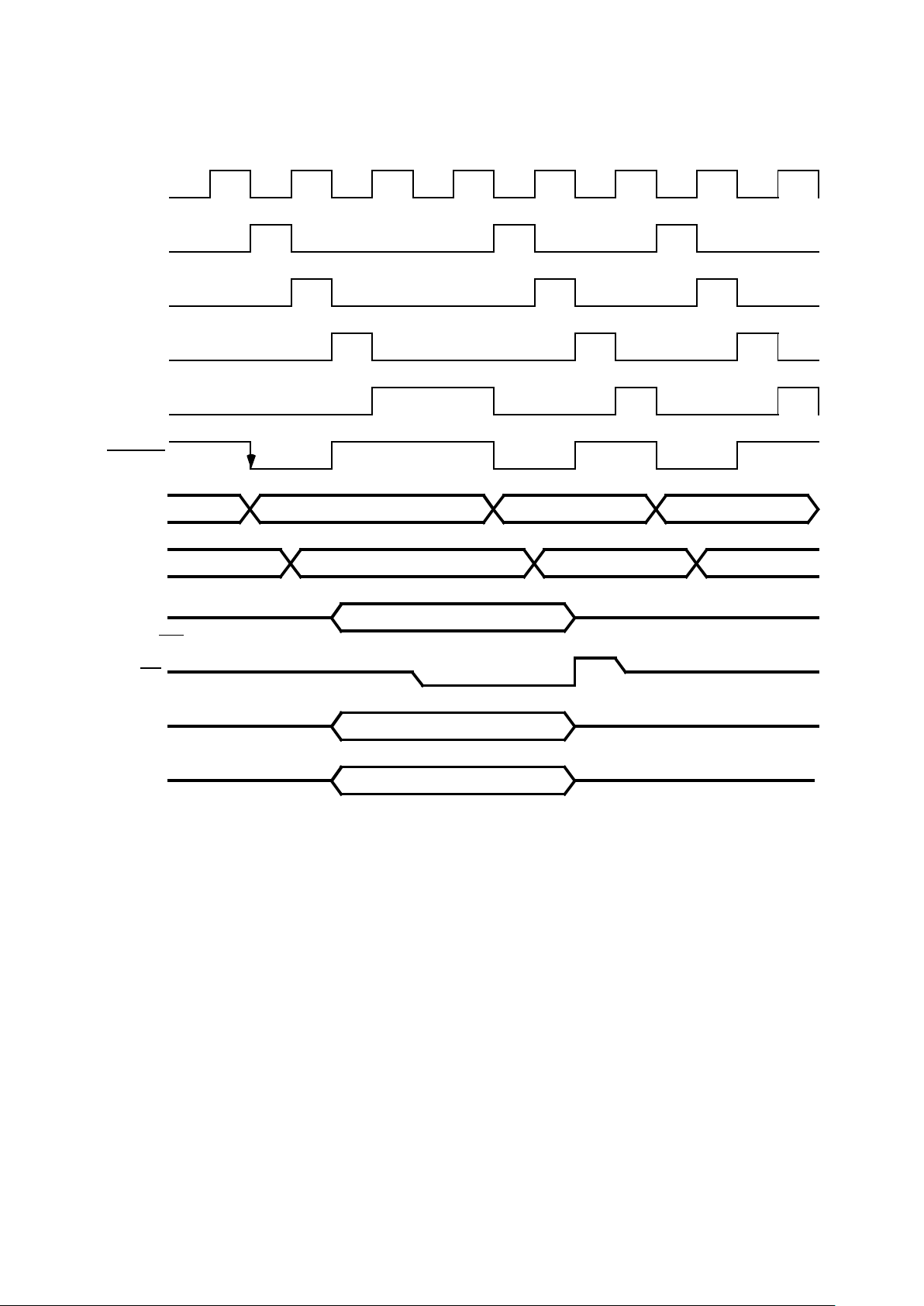
Figures 24, 25, and 26 display the latency associated with
servicing of interrupts. When an interrupt is sampled into the
UT69R000 before the falling edge of STATE1 (figure 24)
interrupt service begins during the following execute machine
cycle (STATE1 low). If the interrupt is sampled into the
UT69R000 after the falling edge of STATE1 (figure 26)
interrupt service is delayed one execution cycle. Interrupts are
first sampled into the device and then latched into the PI
Register.
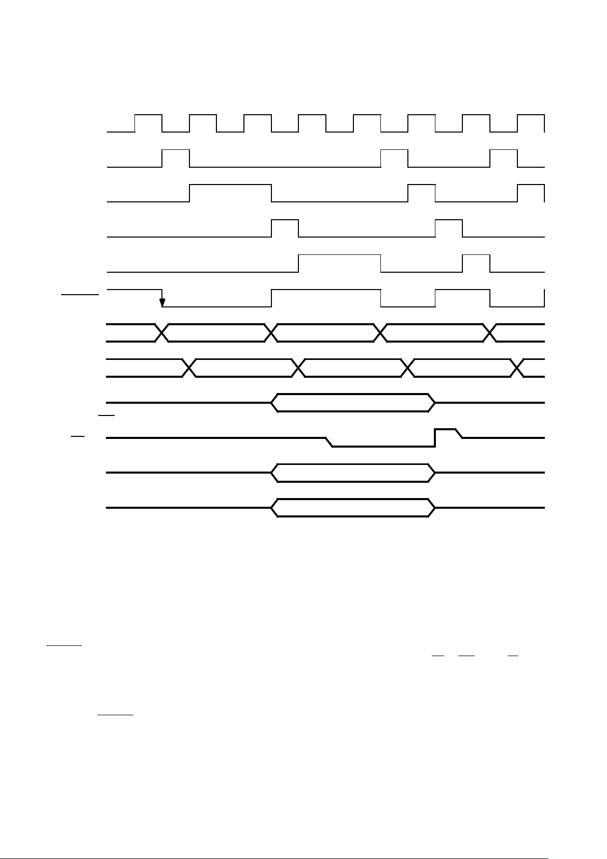
When the interrupt is latched coincident with the fetch and
execution of a CALL instruction the interrupt latency increases.
Figure 25 shows interrupt latency associated to the CALL
instruction. The increase in interrupt latency is due to the
temporary disable of the latching of interrupts into the PI
register. This temporary disable is due to the fetch of the CALL
instruction. The disable is necessary to allow for the UT69R000
to execute the CALL instruction before servicing the
interrupt.7.0 Monitor
7.0 Monitor
Communication between the UT69R000 and a dumb terminal
or IRSIM is established via a monitor program written to
support the internal UART. When operating in the monitor
mode the programmer can (1) examine and modify the
UT69R000’s internal registers; (2) examine and modify the
contents of the operand port memory; (3) examine and modify
the contents of I/O subsystems; (4) control program execution.
UTMC offers a monitor shell program for the UT69R000. The
software programmer can tailor the monitor program to meet
specific application.
Assertion of a discrete input can signal the UT69R000 to enter
the monitor mode of operation. To perform this function the
application software polls the Status Register looking for the
assertion (i.e., transition to logic one) of the appropriate
discrete input. The UT69R000 then enters the monitor program
via a CALL or BR instruction. Interrupts can also be used to

29
access the monitor program. An example of this technique is
accessing the monitor on a specific condition. A specific
interrupt event (e.g., memory access location 100) can generate
a hardware interrupt to the PFAIL input. Accessing the monitor
allows the software programmer to evaluate the state of the
UT69R000 and system (i.e., memory or I/O subsystem).
Figures 27 and 28 show an example.
7.1 Using The Monitor
When the UT69R000 enters the Monitor mode, it begins
executing the monitor program stored in the instruction port.
The UT69R000 initially sets its internal UART as the default
monitor interface.
To control the UT69R000 with the Monitor, the user simply
transmits a predefined set of ASCII characters over the serial
data port. The list of the predefined ASCII characters
meaningful to the UT69R000’s Monitor mode are described in
detail in the following sections. The UT69R000 can receive
these Monitor control commands with its internal UART,
decode them, and then take the appropriate action. All ASCII
characters must be capitalized for the UT69R000 to
recognize them.
The four primary ASCII control characters are E, M, C, and R.
These control characters permit the system user to Examine or
Modify instruction memory, Operand memory, external I/O,
and internal registers, Continue Execution, and Run From a set
starting location.
OSCIN
CK1
CK2
CK3
CK4
EXECUTE
(NOP)
PIR OPEN
PIR CLOSE
EXECUTE
INTERRUPT SERVICE
COMMANDS
PRIMARY INSTRUCTION REGISTER
(PIR)
FETCH
(NOP)
STATE
RA(19:0)
RD(15:0)
INT
INTERRUPT
ADDRESS VALID
INTERRUPT
INSTRUCTION VALID
Figure 24. Interrupt Timing
Assumes:
1. Interrupts enabled at time zero.
2. No mask bits set at time zero. Do not care field
Do not care field
#

30
OSCIN
CK1
CK2
CK3
CK4
EXECUTE
(CALL)
EXECUTE
(NOP)
INTERRUPTS DISABLED DUE TO FETCH
OF CALL OR JMP
INSTRUCTION
FETCH
(CALL)
INTERRUPT
ADDRESS VALID
INTERRUPT
INSTRUCTION VALID
RA(19:0)
RD(15:0)
FETCH
(NOP)
EXECUTE
INTERRUPT SERVICE
COMMANDS
Figure 25. Interrupt Timing
STATE1
INT
Assumes:
1. Interrupts enabled at time zero.
2. No mask bits set at time zero.
Do not care field
Do not care field
#

31
OSCIN
CK1
CK2
CK3
CK4
EXECUTE
(ENOP)
PIR OPEN PIR CLOSE
RA(19:0)
RD(15:0)
EXECUTE
INTERRUPT SERVICE
COMMANDS
PRIMARY INSTRUCTION REGISTER (PIR)
FETCH
(NOP)
FETCH
(INR)
EXECUTE
(INR)
INTERRUPT
ADDRESS VALID
INTERRUPT
INSTRUCTION VALID
Figure 26. Interupt Timing
STATE1
INT
Assumes:
1. Interrupts enabled at time zero.
2. No mask bits set at time zero.
Do not care field
Do not care field
#

32
PROGRAM
CODE
XXXXX(hex)
XXXXX(hex)
EXTERNAL HARDWARE INTERRUPT
OR OUTPUT DISCRETE:
IC ICS
IC INTERRUPT MAP ADDRESS
4XX (HEX)
INTERRUPT SERVICE ROUTINE:
4XX (hex) INR xR16, ICS ;SAVE ICS
4XX (hex) CALL xR18, MONITOR ; MONITOR CODE
4XX (hex) MONITOR
4XX (hex) NOP
Figure 27. Monitor Operation
Monitor Mode
UT69R000
UART PORT
CONSOLE
TERMINAL
UT69R000
MONITOR
RS-232 Port
Examine
(EI, EO, EE, ER)
Continue
(C0, C1, C2, C3)
Run
(R0, R1, R2, R3)
Modify
(MI, MO, ME, MR)
Figure 28. Monitor Mode Operation

33
7.1.1 Examine Command
The Examine Command has four variations:
(1) EIxxxx - The Examine Instruction memory command.
This command permits the user to examine any memory
location within the 64K instruction memory space. The
EI command is followed by the 16-bit Hex address, above
as “xxxx,” of the memory location to examine. Valid
characters for the instruction address field (xxxx) are 09 and A-F.
The user can examine consecutive memory locations by
repeatedly entering Space characters. The Monitor
continues to display the contents of contiguous memory
locations until any non-Space character is received. When
the Monitor receives a non-Space character, it terminates
EI command execution and waits for the next valid
Monitor command.
(2) EOxxxx - The Examine Operand memory command.
This command works exactly the same as the EI
command except that the user can now examine Operand
memory.
(3) EExxxx - The Examine External (I/O) command. This
command works exactly the same as the EI and EO
commands except that the user can now examine any
external I/O location.
(4) ER - The Examine Register command. The Examine
Register command allows the user to look at most of the
UT69R000’s internal registers.
After the UT69R000 has received the ER command, it
displays the contents of register R0. The user can examine
additional registers by repeatedly transmitting Space
characters to the UT69R000. The Monitor displays the
registers one after another in the following order: R0
through R15, Status/Output Discrete register (SW),
Pending Interrupt Register (PI), Interrupt Mask Register
(MK), Fault Register (FT), Timer A (TA) and Timer B
(TB). The UT69R000 continues to display its registers
until the UT69R000 receives a non-Space character
oruntil the UT69R000 has displayed the complete list of
registers. At this time the UT69R000 terminates the ER
command and waits for the next valid Monitor command.
7.1.2 Modify Command
The Modify Command has four variations:
(1) MIxxxx,vvvv - The Modify Instruction memory
command. This command permits the user to modify any
memory location within the 64K instruction memory
space. The MI command is followed by the 16-bit Hex
address denoted above as “xxxx,” of the memory location
to examine and the 16 bit Hex value denoted above as
“vvvv,” the user wishes to place in this memory location.
Valid characters for the instruction address field (xxxx)
and value field (vvvv) are 0-9 and A-F.
The user can modify consecutive memory locations by
entering multiple 16-bit values in the MI command. The
MI command would then take the form:
MIxxxx,vvvv,vvvv,...,vvvv where the user can enter as
many new values as desired. The commas are optional as
delimiters. The UT69R000 now modifies instruction
memory starting at the given address (xxxx) and
continues to modify memory until all new values are
in memory.
(2) MOxxxx,vvvv - The Modify Operand memory
command. This command works exactly the same as the
MI command except that the user can now modify
Operand memory. The form of the MO command to alter
multiple Operand memory locations is:
MOxxxx,vvvv,vvvv,...,vvvv.
(3) MExxxx,vvvv - The Modify External I/O command. This
command works exactly the same as the MI and MO
commands except that the user can now modify any
external I/O location. The form of the ME command to
alter multiple external I/O locations is:
MExxxx,vvvv,vvvv,...,vvvv.
(4) MRrr,vvvv - The Modify Register command. The Modify
Register command allows the user to modify most of the
UT69R000’s internal registers. The MR command is
followed by an 8-bit register ID code, denoted as rr, and
a 16-bit value, denoted as vvvv. Table 4 lists the register
IDs that the UT69R000 recognizes. Valid characters for
the register ID field (xxxx) and value fields (vvvv) are
0-9 and A-F.
The user can use only one MR command to modify one
UT69R000 register. Modifying additional registers
requires transmitting a separate MR command for
each change.

34
7.1.3 Continue Command
The Continue Execution Command allows the user to resume
program execution from the point where the Monitor mode of
operation was entered. The Continue Execution command
takes the form:
C0-Resume execution with Timers A and B halted.
C1- Resume execution with Timer A on and Timer B off.
C2 - Resume execution with Timer A off and Timer B on.
C3- Resume execution with Timers A and B on.
7.1.4 Run Command
The Run From Memory Location Command allows the user to
start program execution from any point within the 1M port
space. This command takes the form Rxxxxn where “xxxxx”
denotes the 20-bit starting address. Valid characters for the
address field (xxxx) are 0-9 and A-F. The value n is either 0,1,2,
or 3 and is defined:
0 - Resume execution with Timers A and B halted.
1 - Resume execution with Timer A on and Timer B off.
2 - Resume execution with Timer A off and Timer B on.
3 - Resume execution with Timers A and B on.
8.0 UART Operation
The UT69R000 has an internal UART. Figure 29 shows a
diagram of the UT69R000 connected to a serial bus. The UART
operates at a fixed frequency of 9600 baud with eight bits, one
stop bit, and odd parity. The idle state for the UART is logic
zero. The TIMCLK input fixes the baud rate of the UART
(9600 baud at TIMCLK equal to 12 MHz). TIMCLK also
controls the frequency of the internal timers (TA and TB). The
status of the UART is read from the System Status Register
(STATUS) bits 7 through 0.
8.1 UART Transmitter Operation
The transmitter portion of the UT69R000’s UART is a doublebuffered configuration consisting of a Transmitter Register and
a Transmitter Buffer Register. The Transmitter Register
contains the serial data stream the UT69R000 is currently
transmitting through the UART; the Transmitter Buffer
Register contains the next message to transmit through the
UART. The system programmer reads the status of the
Transmitter Register from bit 1 (TE) of the Status and the status
of the Transmitter Buffer Register from bit 2 (TBE) of the
Status Register. If bit 2 of the Status register is a logical one,
the UART transmitter buffer is ready for data, once loaded with
data, bit 2 transitions to a logical zero. Bit 1 is a logical zero
during serial transmission and transitions to a logical one when
transmission from the Transmitter Register is complete. The
Status register is read using Input Register Instruction INR
Rd,STATUS.
To initiate a serial data transmission, the system designer must
first load the data to transmit into the Transmitter Buffer
Register with the Output Register Instruction OTR Rd, TXMT.
This instruction loads the least significant byte of the source
register specified in the instruction into the Transmitter Buffer
Register. At this time, TBE goes low and the UT69R000
automatically transfers the data word into the Transmitter
Register. After the transfer is complete, TE goes low and TBE
transition to a logical one indicating a serial transmission is
about to begin and the next data word can be loaded into the
Transmitter Buffer Register.
Figure 29. Serial Data Bus Interface to the UT69R000
AND ODD PARITY
ONE STOP BIT
EIGHT DATA BITS,
9600 BAUD
SERIAL RS-232 BUS X0106-
RCVR
BUS
SERIAL
DRVR
BUS
SERIAL
UT69R000
FOR UART
12 MHz I/P
TIMCLK
UARTIN
UARTOUT

35
This double-buffering process allows transmitting contiguous
serial data streams. The process of alternately loading the
Transmitter Buffer Register with new data and then reading the
transmitter status from the STATUS register continues until
completion of all serial transmission. An example of UART
transmitter software follows:
WRITE_UART: INR R11, STATUS
TBR R11, 1DH
BR EQ, WRITE_UART
NOP
INR R15, TXMT
8.2 UART Receiver Operation
The UT69R000’s internal UART has one register associated
with the receive function. This register is the UART Receiver
Buffer Register (RBR). The least significant byte of the RCVR
contains the received serial data. The Status Register contains
error information about the serial data in the receiver. Four
error bits reflect information status, bit 7 (Receiver Error, RE),
which is the logical OR combination of the other three error
bits; bit 6 (Overrun Error, OE); bit 5 (Framing Error, FE); bit
4 (Parity Error, PE). An additional status bit for the Receiver
is the Data Ready (DR) bit. DR is the least significant bit of
the Status Register.
The UT69R000 is ready to receive serial data through the
internal UART, it must poll the Status Register to determine
when the Data Ready (DR) bit transitions from a logical zero
to logical one to signal the UART has indeed received a serial
transmission. When DR equals a logic one, the software reads
the Receiver by executing and Input Register Operation INR
RD, RCVR. The INR instruction takes the eight bits of received
data in the and places this data in the least significant byte of
the destination register (Rd) specified in the instruction.
When the UT69R000 is finished executing the Input Register
Instruction, the software can then determine the validity of the
message by testing the RE bit. After the software has checked
for a valid message, the data is stored. If the UT69R000 is to
receive more data through the UART, the software must return
to polling the Status Register to determine the reception of the
next valid serial transmission. The Input Register Instruction
INR Rd, RCVR clears the DR bit. An example of receiver
software follows:
READ_UART: INR R11, STATUS
TBR R11, 1FH
BR EQ, READ_UART
NOP
OTR R15, RCVR 9.0
9.0 PROGRAMMING INTERFACE
9.1 Data Formats
The UT69R000 instruction set supports 16-bit integer singleprecision data and 32-bit integer double-precision data. All data
is in 2’s complement representation.
The UT69R000 represents the fixed-point data formats as a 2’s
complement integer with the MSB as the sign bit (figures 30a
and 30b).
Operand Size
The UT69R000’s instruction set supports three operand sizes:
(1) Byte (eight bits); (2) Word (16 bits); and (3) Long Word
(32 bit). Byte operands are only allowed with byte instructions.
All other instructions support word and long-word operands.
Organization of Data in General Purpose Registers
All 20 of the UT69R000’s general purpose data registers
support bit, byte, and word operations. When the system
programmer specifies a byte operation in a specific instruction,
the instruction expects to find the byte of Operand Data in the
least significant eight bits of the data register. The least
significant bit of each of the data registers is bit 0 and the most
significant bit of each of the data registers is bit 15. Any one
of the data registers may be the source or destination for the
operand.
For long-word operands, the UT69R000 organizes the 20
general purpose data registers as 10 even/odd register pairs.
The even-numbered register of the register pair contains the
most significant word. All register pairs may be the source or
destination operands.
14 0
Figure 30a. Single-Precision Fixed-Point Data
Figure 30b. Double-Precision Fixed-Point Data
15
SIGN DATA
LSBMSB
SIGN
MSB LSB
(MSH) (LSH)
31 30 16 15 0

36
Special Purpose Data Registers
In addition to the 20 general purpose data registers, the
UT69R000 has three special purpose data registers: (1) The
ACCUMULATOR (ACC); (2) the Stack Pointer (SP); and (3)
the Instruction Counter Save Register (ICS).
The Accumulator (ACC) is a 32-bit register used only with
multiply, divide, extended shift, Load Register from
Instruction memory (LRI), and Store Register to Instruction
memory (STRI) instructions. For multiply instructions, the
ACC retains the most significant half of the product, and for
divide instructions, the ACC retains the remainder. For LRI
and STRI instructions, the ACC contains the instruction
memory pointer. Note that the ACC can be used as a general
purpose register for most operations.
The Stack Pointer (SP) is a 16-bit register usable only with POP
and PUSH instructions.
The Instruction Counter Save (ICS) register is a 20-bit register
used during calls, jumps, and interrupts.
Register Notation
The UT69R000’s instruction descriptions contain a definition
of the Register Transfer Language (RTL) that the Assembler
uses to describe how the instructions operate. The RTL
description of the UT69R000’s internal registers is as follows:
RSn -- Source Register where n specifies the
register number.
RDn -- Destination Register where n specifies the
register number.
XRSn -- Long-Data Source Register where n specifies the
register number.
XRDn -- Long-Data Destination Register where n specifies
the register number.
IC -- Instruction Counter
SP -- Stack Pointer
ACC -- 32 bit Accumulator
ICS -- Instruction Counter Store Register
@RSn -- Data Register Indirect where n specifies the
register number
@SP -- Stack Pointer Indirect
# -- Immediate Data
@# -- Immediate Data Indirect
9.2 Instruction Formats
The UT69R000 has three instruction formats (figure 32): (1)
Register-to-Register; (2) Register-to-Short Immediate; and (3)
Register-to-Immediate.
All the UT69R000’s instructions are either word (16-bit) or
long-word (32-bit) in length. The only time the UT69R000 uses
the long-word instruction format is for the Immediate Source
Operand Address Mode.
The bits in the instructions are defined as follows:
M: Instruction Mode Bit. When M = 1, the UT69R000
interprets the Instruction Source field as a five-bit literal
value. If M = 0, the UT69R000 uses the Instruction Source
field to specify the source register for the instruction.
Opcode: This field is the five-bit opcode the UT69R000
uses to decode the instruction into a machine operation.
0459101415
Figure 31b. Register to-Short Immediate
0459101415
Figure 31a. Register to-Register Instruction
Figure 31c. Register Immediate Instruction Format
MSB
LSB
MODE OPCODE DESTINATION SOURCE
0 XXXXX RD RS
MODE OPCODE DESTINATION SOURCE
MSB LSB
1 XXXXX RD IMMEDIATE
MODE
MSB
OPCODE DESTINATION SOURCE
LSB
0 XXXXX RD 11111
0459101415
16-Bit Immediate Data
15 0
MSB LSB
Instruction Format

37
Destination: This field specifies the register the UT69R000
uses for the destination of the instruction.
Source: This field specifies the register the UT69R000 uses
for the Instruction Source.
Immediate: If needed, this field contains the 16-bits of
immediate data the UT69R000 requires for the longimmediate instruction.
9.3 Operand Addressing Modes
The UT69R000’s instruction set supports four basic addressing
modes. All instructions require a source operand and a
destination operand. The destination operand is a data register
(RDn or XRDn) for all instructions, except the Jump on
Condition (JC) instruction where the destination register
contains a template for the jump condition tested for in the
instruction. The source operand can be either a data register or
immediate data for all instructions.
The source operand can also be addressed in an indirect mode.
In an indirect addressing mode, the source data register or the
Stack Pointer contains an effective address. This address points
to the memory location for operand data the UT69R000 uses
during the current instruction execution. This type of memory
addressing is only used with the Load (LR), Store (STR),
PUSH, and POP instructions.
Destination Addressing Mode
The destination operand is given explicitly for all UT69R000
instructions. The UT69R000 encodes a five-bit field, bits 9
through 5, in each instruction as follows:
R0 -- 00000 XR0 -- 10000
R1 -- 00001 R16 -- 10001
R2 -- 00010 XR2 -- 10010
R3 -- 00011 R17 -- 10011
R4 -- 00100 XR4 -- 10100
R5 -- 00101 XR16 -- 10110
R6 -- 10110
R7 -- 00111 XR8 -- 11000
R8 -- 01000 R18 -- 11001
R10 -- 01010 XR10 -- 11010
R11 -- 01011 R19 -- 11011
R12 -- 01100 XR12 -- 11100
R13 -- 01101 XR18 -- 11101
R14 -- 01110 XR14 -- 11110
R15 -- 01111 ACC -- 11111
NUL -- 10111
Source Addressing Modes
The UT69R000 directly addresses the source operand by using
one of three normal modes: (1) Data Register Direct; (2)
Literal; and (3) Immediate Long Data.
Data Register Direct
When the UT69R000 uses the Data Register Direct mode, the
source operand is one of the data registers. The data register is
explicitly stated for all instructions. The UT69R000 encodes
a 5-bit field, bits 4 through 0, in each instruction as follows:
R0 -- 00000 XR0 -- 10000
R1 -- 00001 R16 -- 10001
R2 -- 00010 XR2 -- 10010
R3 -- 00011 R17 -- 10011
R4 -- 00100 XR4 -- 10100
R5 -- 00101 XR16 -- 10101
R6 -- 00110 XR6 -- 10110
R7 -- 00111
R8 -- 01000 XR8 -- 11000
R9 -- 01001 R18 -- 11001
R10 -- 01010 XR10 -- 11010
R11 -- 01011 R19 -- 11011
R12 -- 01100 XR12 -- 11100
R13 -- 01101 XR18 -- 11101
R14 -- 01110 XR14 -- 11110
R15 -- 01111 Reserved -- 10111
and 11111
Literal
When the UT69R000 uses the Literal mode, the source operand
is a 5-bit literal data value. The UT69R000 explicitly states this
literal data value for the instructions. The UT69R000 encodes
a 5-bit field, bits 4 through 0, in each instruction as follows:
0 -- 00000 -16 -- 10000
+1 -- 00001 -15 -- 10001
+2 -- 00010 -14 -- 10010
+3 -- 00011 -13 -- 10011
+4 -- 00100 -12 -- 10100
+5 -- 00101 -11 -- 10101
+6 -- 00110 -10 -- 10110
+7 -- 00111 - 9 -- 10111
+8 -- 01000 - 8 -- 11000
+9 -- 01001 - 7 -- 11001
+10 -- 01010 - 6 -- 11010
+11 -- 01011 - 5 -- 11011
+12 -- 01100 - 4 -- 11100
+13 -- 01101 - 3 -- 11101
+14 -- 01110 - 2 -- 11110
+15 -- 01111 - 1 -- 11111
Immediate Long
When the UT69R000 uses the Immediate Long mode, the
source operand is a 16-bit data value. The UT69R000 explicitly
states this data for all instructions and encodes the 16-bit data
in a second 16-bit instruction word (figure 32). The UT69R000
encodes the 5-bit field of the instruction source field, bits 4
through 0, as follows:
IMM -- 11111

38
Special Source Operand Addressing Modes
In addition to its three direct addressing modes, the UT69R000
also supports three modes of indirect addressing: (1) Data
Register Indirect; (2) Stack Pointer Indirect; and (3) Absolute.
Data Register Indirect
When the UT69R000 uses the Data Register Indirect mode, the
source operand is a memory location addressed by the contents
of the specified data register. The data register is explicitly
stated for all instructions. This mode is only available on the
LR, STR, INR, and STR instructions. The UT69R000 encodes
a 5-bit field, bits 4 through 0, in each instruction as follows:
R0 -- 00000 XR0 -- 10000
R1 -- 00001 R16 -- 10001
R2 -- 00010 XR2 -- 10010
R3 -- 00011 R17 -- 10011
R4 -- 00100 XR4 -- 10100
R5 -- 00101 XR16 -- 10101
R6 -- 00110 XR6 -- 10110
R7 -- 00111
R8 -- 01000 XR8 -- 11000
R9 -- 01001 R18 -- 11001
R10 -- 01010 XR10 -- 11010
R11 -- 01011 R19 -- 11011
R12 -- 01100 XR12 -- 11100
R13 -- 01101 XR18 -- 11101
R14 -- 01110 XR14 -- 11110
R15 -- 01111 Reserved -- 10111
and 11111
Stack Pointer Indirect
When the UT69R000 uses the Stack Pointer Indirect mode, the
source operand is a memory location addressed by the contents
of the Stack Pointer (SP) register. This mode is only available
with POP and PUSH instructions. The UT69R000 encodes a
5-bit field, bits 11 through 15, of each instruction when in the
Stack Pointer Indirect mode as follows:
SP -- 10111.
Absolute
When the UT69R000 uses the Absolute mode, the source
operand is the memory location addressed by the contents of
the 16-bit immediate-data field accompanying the instruction.
This mode is only available on the LR, STR, INR, and OTR
instructions. The system programmer encodes the immediate
data field as a second 16-bit instruction word.
9.4 Data Movement Operations
The UT69R000 places no restrictions on operand size during
data movement. This means the size (Byte, Word, or Long
Word) of the data in the source and destination do not have to
match. The UT69R000 handles the data movement for all
instructions.
When a instruction specifies a word destination, a 16-bit result
is always stored in the destination. If the instruction specifies
a 5-bit literal source operand, then the UT69R000 sign-extends
this source data to produce a 16-bit operand. If the instruction
specifies a word-length source operand, there is no
manipulation of the source data. If the instruction specifies a
long-word source operand, the UT69R000 only retains the least
significant 16 bits of the result. The UT69R000 truncates the
most significant 16 bits of the result.
When a instruction specifies a long-word destination, a 32-bit
result is always stored in the destination. If the instruction
specifies a 5-bit literal source operand, then the UT69R000
sign-extends this source data to produce a 32-bit operand. If
the instruction specifies a word-length source operand, then the
UT69R000 also sign-extends this source data to produce a 32bit operand. If the instruction specifies a long-word-length
source operand, there is no manipulation of the source data.
When the system programmer specifies a byte instruction, the
UT69R000 only stores eight bits of the result regardless of
whether the instruction specifies a word or long-word
destination register.
Operation Code Matrix
The UT69R000 performs 30 basic operations, each with its
own operation code. All the UT69R000’s operations are
explicit, and are encoded in bits 14 through 10 of the
instruction.

39
10.0 PIN DESCRIPTION
Legend for TYPE and ACTIVE fields:
TO = TTL output
TI = TTL input
TUI = TTL input (pull-up)
TDI = TTL input (pull-down)
TTO = Three-state TTL output
TTB = Three-state TTL bidirectional
CO = CMOS output
OSC = Oscillator input to a Pierce Oscillator
inverter
AH = Active High
AL = Active Low
OSCIN 50 P14 OSC
OSCILLATOR AND CLOCK SIGNALS
PIN NAME
PIN NUMBER
FLTPK PGA
TYPE ACTIVE DESCRIPTION
OSCOUT
SYSCLK
51
52
P15
M14
CO
TO
Oscillator Input. A 50% duty cycle crystal-drive input
for driving the UT69R000.
Oscillator Output. A 50% duty cycle, single-phase clock
output at the same frequency as the OSCIN input.
System Output. The buffered equivalent of the
OSCOUT signal.
NUI1 129 H2 TI
PROCESSOR STATUS
PIN NAME
PIN NUMBER
FLTPK PGA
TYPE ACTIVE DESCRIPTION
NUI2
NUO3
44
126
P12
G3
TUI
TTO
Not used input 1. Internal UTMC use only. Tie either
high or low.
Not used input 2. Internal UTMC use only. Tie low.
Not used output 3. Internal UTMC use only. NUO3 enter
high impedance state when the UT69R000 is in the test
mode (TEST=0)
--
--
--
NUI3 45 N11 TDI
--
Not used input 3. Internal UTMC use only. Tie low.
54 N15 TTO
Processor State. This signal indicates the internal state
of the UT69R000. A low on STATE1 indicates the
UT69R000 is executing a new instruction. A high on
STATE1 indicates the UT69R000 is fetching an
instruction. STATE1 enters a high-impedance state
when the UT69R000 is in the test mode ( TEST=0).
--
--
--
--
NUI4 61 K15 TUI
Not used input 4. Internal UTMC use only. Tie high.
--
STATE1
NU01 115 C3 TTO
Not used output 1. Internal UTMC use only.
--
NU02 113 A2 TTO
Not used output 2. Internal UTMC use only.

40
118 D2 TTO
OPERAND DATA BUS ARBITRATION
PIN NAME
PIN NUMBER
FLTPK PGA
TYPE ACTIVE DESCRIPTION
119
120
E3
C1
TUI
TUI
Bus Request. The UT69R000 asserts this signal to indicate
it is requesting control of the Operand data bus (D0 - D15).
BRQ enters a high-impedance state when the UT69R000
is in the test mode ( TEST = 0).
Bus Grant. When asserted, this signal indicates the
UT69R000 may take control of the Operand data bus. It is
tied to an internal pull-up resistor.
Bus Busy. A bus master asserts this input to inform the
UT69R000 that another bus master is using the Operand
data bus. It is tied to an internal pull-up resistor.
OPERAND DATA BUS CONTROL
PIN NAME
PIN NUMBER
FLTPK PGA
TYPE ACTIVE DESCRIPTION
121
112
E2
B3
TUI
TTO
Data Transfer Acknowledge. This signal tells the
UT69R000 that a data transfer has been acknowledged
and the UT69R000 can complete the bus cycle. To
assure the UT69R000 operates with no wait states,
DTACK can be tied low. DTACK is tied to an internal
pull-up resistor.
Memory or I/O. Indicates whether the current bus cycle
is for memory (high) or I/O (low). It remains in the highimpedance state during bus cycles when the UT69R000
does not control the Operand buses.
AL
117 B1 TTO AL
AL
AL
AL
Bus Grant Acknowledge Output. The UT69R000 asserts
this signal to indicate it is the current bus master. When
low, BGACK inhibits other devices from becoming the
bus master. When the UT69R000 relinquishes control of
the bus, BGACK enters a high-impedance state.
114 C4 TTO Read/Write. Indicates the direction of data flow with
respect to the UT69R000. R/WR high means the
UT69R000 is attempting to read data from an external
device, and R/WR low means the UT69R000 is
attempting to write data to an external device. R/ WR
remains in a high-impedance state when the UT69R000
does not control the Operand buses.
Continued on page 41.
--
--
BRQ
BGNT
BUSY
BGACK
DTACK
M/IO
R/WR

41
Output Enable Instruction Memory. This signal
allows memory to place data on the instruction data bus.
The Store Register to Instruction Memory (STRI)
instruction removes OE during the CK2 internal clock
cycle. OE enters a high-impedance state when the
UT69R000 is in the test mode (TEST = 0).
OPERAND DATA BUS CONTROL
PIN NAME
PIN NUMBER
FLTPK PGA
TYPE ACTIVE DESCRIPTION
116 B2 TTO
Data Strobe. Indicates valid data is on the Operand Data
bus. The UT69R000 places DS in a high-impedance state
when it does not control the Operand buses.
42 R12 TTO
INSTRUCTION MEMORY CONTROL
PIN NAME
PIN NUMBER
FLTPK PGA
TYPE ACTIVE DESCRIPTION
43 R13
TTO
Write Enable Memory. This signal allows the
UT69R000 to write to instruction memory. The Store
Register to Instruction Memory (STRI) instruction
asserts WE during the CK2 internal clock cycle. WE
enters a high-impedance state when the UT69R000 is in
the test mode (TEST = 0).
AL
AL
Continued from page 40.
AL
UART CONTROL/TIMER CLOCK
UARTIN 127 F1 TUI
PIN NAME
PIN NUMBER
FLTPK PGA
TYPE ACTIVE DESCRIPTION
UARTOUT 128 G1 TTO
AH
AH
UART Input. The UT69R000 receives serial data
through this input. The serial data is stored in the
UT69R000’s Receiver Buffer Register (RCVR). It is
tied to an internal pull-up resistor.
UART Output. The serial data stored in the UT69R000’s
Transmitter Buffer Register (TXMT) is transmitted
through this output. The UART output is fixed at 9600
baud, with eight data bits, odd-parity, and one stop bit.
UARTOUT enters a high-impedance state when the
UT69R000 is in the test mode (TEST=0). (9600 baud @
TIMCLK = 12 MHz)
Continued on page 42.
WE
OE
DS

42
Test (Input). Asserting this input places the UT69R000
into a test mode. In this mode, all the UT69R000’s
outputs, except OSCOUT and SYSCLK, enter a highimpedance state. When using TEST, the UT69R000
must have a MRST. MRST must be held active for at
least one SYSCLK period after TEST is deasserted to
assure proper operation (see figure 41b). TEST is tied
to an internal pull-up resistor.
TIMCLK 53 L13 TI
UART CONTROL/TIMER CLOCK
PIN NAME
PIN NUMBER
FLTPK PGA
TYPE ACTIVE DESCRIPTION
DI2 48 N12 TDI
Timer Clock. This 12 MHz clock input generates the baud
rate for the UT69R000’s internal UART. The input also
provides the clock for the UT69R000’s two internal timers
(TIMER A and TIMER B).
Discrete Input 2. Asserting this input sets bit 3 in the
System Status Register Bit 3 is read with the Input Register
Instruction (INR). Tied to an internal pull-down resistor.
(asynchronous input).
TEST 46 P13 TUI
DI1 49 N13 TDI
--
Discrete Input 1. Asserting this input sets bit 8 in the
System Status Register. Bit 8 is read with the Input
Register Instruction (INR). Tie to a internal pull-down
resistor. (asynschronous input).
--
Continued from page 41
AL
PROCESSOR MODE
OD0 104 B7 TTO
PIN NAME
PIN NUMBER
FLTPK PGA
TYPE ACTIVE DESCRIPTION
OD4 108 A4
--
Output Discrete Bus (OD(7:0)). These outputs reflect
the status of bits 0 through 7 of the Status/Output
Discrete Register. Write to this register using Output
Register Instruction (OTR). Outputs enter a highimpedance state when the UT69R000 is placed in the
test mode (TEST = 0).
OD1
OD2
OD3
105
106
107
B6
C6
A5
OD5
OD6
OD7
109
110
111
A3
B4
C5
--

43
Memory Parity (Error). Asserting this input indicates a
machine error. Bit 13 of the UT69R000’s Fault
Register, is set when MCHNE2 is active. Under no
circumstances should MCHNE2 be tied in its active
state. It is tied to an internal pull-down resistor. Interrupt
is not cleared via software until the negation of the input
signal.
MCHNE1 125 G2 TUI
INTERRUPTS/EXCEPTIONS
PIN NAME
PIN NUMBER
FLTPK PGA
TYPE ACTIVE DESCRIPTION
122 D1 TUI
System Fault. This positive edge-triggered input sets bit 8
(MCHNE1) in the UT69R000’s Fault Register. Under no
circumstances should MCHNE1 be tied in its active state.
It is tied to an internal pull-up resistor. Interrupt is not
cleared via software until the negation of the input signal.
MCHNE2
Bus Time Error. It is asserted when a bus error or a timeout
occurs. During I/O bus cycles, an active BTERR sets bit
10 of the Fault Register. During Memory bus cycles, an
active BTERR sets bit 7 of the Fault Register. Under no
circumstances should BTERR be tied in its active state. It
is tied to an internal pull-up resistor. Interrupt is not cleared
via software until the negation of the input signal.
124 F2 TDI
MPROT 123 F3 TUI
AH
Memory Protect Fault. When asserted, it informs the
UT69R000 that a memory-protect fault has occurred on the
Operand Data Bus. An access fault, a write-protect fault, or
an execute-protect fault causes a memory-protect fault. If the
UT69R000 is using the bus and MPROT is asserted, bit 15
of the Fault Register (CPU Fault) is set. If the UT69R000 is
not using the bus and MPROT is asserted, bit 14 of the Fault
Register (DMA Error) is set. It is tied to an internal pull-up
resistor. Interrupt is not cleared via software until the
negation of the input signal.
AL
AH
56 M15 TUI
62 J15
User Interrupts. These interrupts are active on a negativegoing pulse and each will set, when active, its associated bit
in the Pending Interrupt Register. The interrupts are
maskable by setting the associated bits in the Interrupt Mask
Register. Asserting MRST resets all interrupts. They are
tied to an internal pull-up resistor.
57
58
59
60
K13
K14
J14
J13
63 H14
55 L14 TUI AL Power Fail (Interrupt). Asserting this input
informs the UT69R000 that a power failure has occurred and
the present process will be interrupted. This input sets bit 15
in the Pending Interrupt Register. A Power Fail Interrupt (bit
15) cannot be disabled or masked. It is tied to an internal pullup resistor.
47
R14 TUI AL
Master Reset. This input initializes the UT69R000 to a
reset state. The UT69R000 must be reset after power
(Vcc) is within specification and stable to ensure proper
operation. The system must hold MRST active for at
least one period of SYSCLK to assure the UT69R000
will be reset. It is tied to an internal pull-up resistor.
AH
AL
BTERR
INT0
INT1
INT2INT3
INT4
INT5
INT6
INT2
PFAIL
MRST
61
K15 TUI --
NUI4
Not used input 4. Internal UTMC use only. Tie high.

44
A0 84 A14 TTO
OPERAND BUSES
PIN NAME
PIN NUMBER
FLTPK PGA
TYPE ACTIVE DESCRIPTION
Address Bus - Operand. When asserted, this bus is
unidirectional and represents the Operand Address. The
bus is in the high-impedance state when the UT69R000
does not control the bus. A15 is the most significant bit.
The Operand Address enters a high-impedance state when
the UT69R000 is in the test mode (TEST = 0).
D0 64 H15 TTB
Data Bus - Operand. This bidirectional data bus remains
in a high-impedance state when the UT69R000 does not
control the bus. D15 is the most significant bit. The
Operand Data Bus enters a high-impedance state when
the UT69R000 is in the test mode (TEST = 0).
--
RA0 18 R2 TTO
Instruction Address Bus. This unidirectional bus represents
the address of the data in instruction memory. RA19 is the
most significant bit. The address enters a high-impedance
state only when the UT69R000 is in the test mode (TEST = 0).
A1
A2
A3
A4
A5
A6
A7
A8
A9
A10
A11
A12
A13
A14
A15
85
86
87
88
89
90
91
92
93
94
95
96
97
102
103
B12
C11
A13
B11
A12
C10
B10
B9
C9
A10
A9
B8
A8
A7
A6
D1
D2
D3
D4
D5
D6
D7
D8
D9
D10
D11
D12
D13
D14
D15
69
70
71
72
73
74
75
76
77
78
79
80
81
82
83
G15
F15
G14
F14
F13
E15
D15
C15
D14
E13
C14
B15
D13
C13
B14
--
INSTRUCTION BUSES
PIN NAME
PIN NUMBER
FLTPK PGA
TYPE ACTIVE DESCRIPTION
RA1
RA2
RA3
RA4
RA5
RA6
RA7
RA8
RA9
RA10
RA11
RA12
RA13
RA14
RA15
19
20
21
22
23
24
25
26
27
28
29
30
31
36
37
P4
N5
R3
P5
R4
N6
P6
P7
N7
R6
R7
P8
R8
R9
R10
--
Continued on page 45.
RA16
RA17
RA18
RA19
38
39
40
41
P9
P10
N10
R11

45
PIN NAME
PIN NUMBER
FLTPK PGA
TYPE ACTIVE DESCRIPTION
RD0 130 H1 TTB
Instruction Data Bus. This bidirectional data bus is the
interface with the memory. RD15 is the most significant
bit. The Data Bus enters a high-impedance state only
when the UT69R000 is in the test mode (TEST = 0).
V 34 H3
+5 V DC Power. Power supply input.
--
INSTRUCTION BUSES
PIN NAME
PIN NUMBER
FLTPK PGA
TYPE ACTIVE DESCRIPTION
Continued from page 44.
RD1
RD2
RD3
RD4
RD5
RD6
RD7
RD8
RD9
RD10
RD11
RD12
RD13
RD14
RD15
3
4
5
6
7
8
9
10
11
12
13
14
15
16
17
J1
K1
J2
K2
K3
L1
M1
N1
M2
L3
N2
P1
M3
N3
P2
67
100
132
N9
G13
C7
J3
N8
H13
C8
POWER AND GROUND
V 1
33
66
99
Reference Ground. Zero Volts DC, logic ground.
--
-- --
--
DD
SS

46
11.0 ABSOLUTE MAXIMUM RATINGS (1)
SYMBOL PARAMETER LIMITS UNIT
DC supply voltage
Voltage on any pin
DC input current
Storage temperature
Latchup immunity (2)
-0.3 to +7.0
-65 to +150
V
V
mA
mA
Maximum power dissipation
Maximum junction temperature
Thermal resistance, junction-to-case (3)
600
+175
10
mW
-0.3 to VDD + .3
o
C
o
C
o
C/W
(Referenced to VSS)
V
DD
V
I/O
I
I
T
STG
I
LU
P
D
T
J
Q
JC
+150
+10
12.0 RECOMMENDED OPERATING CONDITIONS
SYMBOL PARAMETER LIMITS UNIT
DC supply voltage
Temperature range
4.5 to 5.5
-55 to +125
V
DC input voltage
V
V
DD
T
C
V
IN
o
C
0 to V
DD
Notes:
1. Stresses outside the listed absolute maximum ratings may cause permanent damage to the device. This is a stress
rating only, and functional operation of the device at these or any other conditions beyond limits indicated in the
operational sections of this specification is not recommended. Exposure to absolute maximum rating conditions for
extended periods may affect device reliability.
2. See discussion of test technique (figure 42).
3. Test per MIL-STD-883, Method 1012.

47
13.0 ELECTRICAL CHARACTERISTICS
VDD = 5.0V±10%; -55°C < TC < +125°C
Notes:
1. Supplied as a design limit but not guaranteed or tested.
2. Not more than one output may be shorted at a time for maximum duration of one second.
3. All inputs with internal pull-ups or pull-downs should be left open circuit, all other inputs tied low or high. TEST input pin asserted.
4. Includes current through input pull-ups. Instantaneous surge currents on the order of 1 ampere can occur during output switching. Voltage supply should be
adequately sized and decoupled to handle a large current surge.
5. Double buffer output pins (i.e., DS, R/WR, M/IO).
6. Functional tests are conducted in accordance with MIL-STD-883 with the following input test conditions: VIH=VIH(min)+20%,-0%; VIL=VIL(max)+0%,-50%,
as specified herein, for TTL or CMOS compatible inputs. Devices may be tested using any input voltage within the above specified range, but are guaranteed to
VIH(min) and VIL(max).
7. Radiation-hardened technology shall have a VIH pre-irradiation of 2.2V.
SYMBOL PARAMETER CONDITION MINIMUM MAXIMUM UNIT
V
IL
Low-level input voltage
6
TTL inputs
OSC inputs
.8
1.2
V
V
V
IH
High-level input voltage
6
TTL inputs
7
OSC inputs
2.0
3.6
V
V
I
IN
Input leakage current
Inputs without resistors
Inputs with pull-down resistors
Inputs with pull-up resistors
VIN = V
DD
or V
SS
VIN = V
DD
VIN = V
SS
-10
80
-900
10
900
-80
µA
µA
µA
V
OL
Low-level output voltage
TTL outputs
OSC outputs
I
OL
= 3.2mA
I
OL
= 6.4mA Note 5
I
OL
= 0.1mA
0.4
0.4
1.0
V
V
V
V
OH High-level output voltage
TTL outputs
OSC outputs
I
OH
= -0.4mA
I
OH
= -0.8mA Note 5
I
OH
= - 0.1mA
2.4
2.4
3.5
V
V
V
I
OZ
Three-state output leakage current
VO = VDD or V
SS
-10
-20 Note 5
+10
+20 Note 5
µA
µA
I
OS
Short-circuit output current
1,2
VDD = 5.5V, VO = 0V to V
DD
-100
-200 Note 5
+100
+200 Note 5mAmA
C
IN
Input capacitance
F = 1MHz @ 0V 10 pF
C
OUT
Output capacitance
F = 1MHz @ 0V 15 pF
C
IO
Bidirectional I/O capacitance
F = 1MHz @ 0V 20 pF
I
DD
Average operating current
1, 4
F = 16MHz, CL = 50pF
F = 12MHz, CL = 50pF
75
50
mA
mA
Q
IDD
Quiescent current
Note 3
1 mA

48
14.0 AC ELECTRICAL CHARACTERISTIC
Figure 32a. Typical Timing Measurements
to data valid
to high Z
to response
to response
to response
INPUT
INPUT
INPUT
INPUT
INPUT
INPUT
INPUT
to high Z
to data valid
to responseINPUT
PARAMETER
h
g
f
e
d
c
b
a
t
t
t
t
t
t
t
t
SYMBOL
h
g
f
e
t
t
t
t
d
b
t
t
t
c
a
t
BUS
OUTPUT
OUT-OF-PHASE
OUTPUT
IN-PHASE
MAX
IL
V
MIN
IH
V
INPUT
MAX
OL
V
MAX
OL
V
OL
V
MIN
OH
V
MIN
OH
V
MIN
OH
V
MAX
IL
V
MIN
IH
V
MAX
*Unless otherwise noted, all AC electrical characteristics are guaranteed by design or characterization.
Note:
50pF including scope
probe and test socket.
90%
Figure 32b. AC Test Loads and Input Waveforms
Input Pulses
10%10%
90%
< 2 ns < 2 ns
50 pF
3 V
0 V
5 V
•
IREF (source)
IREF (sink)
VREF

49
41
45
38
55
42
38
41
38
38
35
45
33
--
0
--
0
--
0
--
0
0
0
0
0
ns
ns
ns
ns
ns
ns
ns
ns
ns
ns
ns
ns
ns330
Figure 33. I/O Read Cycle
Note:
--
--0
26
OSCIN high to address invalid
134ut34t
t34s
t34r
t34n
t34m
t34l
t34j
t34i
t34k
t34h
t34g
t34f
t34b
t34a
VALID
DATA
VALID
ADDRESS
OSCIN
OPERAND
DATA
OPERAND
ADDRESS
SYMBOL PARAMETER
MIN MAX
UNITS
t34a
t34b
Data setup time
Data hold time
t34f
t34g
t34h
t34i
t34j
t34k
t34l
t34m
t34n
t34r
t34s
t34t
t34u ns
ns
*
*
*
*
*Guaranteed by test.
*
*
*
*
*
16 MHz
55
57
50
73
51
50
54
50
50
37
54
39
--
0
--
0
--
0
--
0
0
0
0
0
420
--
--0
34
MIN MAX
12 MHz
STATE1
DS
R/WR
M/IO
OSCIN low to STATE1 high
OSCIN low to STATE1 low
OSCIN low to DS inactive
OSCIN low to DS active
OSCIN high to DS inactive
OSCIN low to DS high Z
OSCIN low to R/WR active
OSCIN low to R/WR high Z
OSCIN low to M/IO low
OSCIN high to M/IO high
OSCIN low to M/IO high Z
OSCIN low to address valid

50
41
45
38
55
42
38
42
38
38
35
45
33
--
0
--
0
--
0
--
0
0
0
0
0
ns
ns
ns
ns
ns
ns
ns
ns
ns
ns
ns
ns
ns330
Figure 34. I/O Write Cycle
60
480
--
OSCIN high to address invalid
OSCIN low to address valid
t35ut35t
t35s
t35r
t35n
t35m
t35l
t35j
t35i
t35k
t35h
t35g
t35f
t35b
t35a
VALID
ADDRESS
OSCIN
OPERAND
DATA
OPERAND
ADDRESS
t35a
t35b
OSCIN low to data valid
OSCIN high to data invalid (high Z)
t35f
t35g
t35h
t35i
t35j
t35k
t35l
t35m
t35n
t35r
t35s
t35t
t35u
540t35v
t35v
ns
ns
ns
VALID
DATA
*
*
*
*
*
*
*
*
*
*
*
SYMBOL PARAMETER
MIN MAX
UNITS
16 MHz
MIN MAX
12 MHz
55
57
50
73
51
50
51
50
50
37
54
39
--
0
--
0
--
0
--
0
0
0
0
0
420
80
640
-720
OSCIN low to STATE1 high
OSCIN low to STATE1 low
OSCIN low to DS inactive
OSCIN low to DS active
OSCIN high to DS inactive
OSCIN low to DS high Z
OSCIN low to R/WR inactive
OSCIN low to R/WR high Z
OSCIN low to M/IO low
OSCIN high to M/IO high
OSCIN low to M/IO high Z
OSCIN high to R/WR high
STATE1
DS
R/WR
M/IO

51
41
45
38
42
38
42
38
38
35
45
33
--
0
--
0
--
0
--
0
0
0
0
ns
ns
ns
ns
ns
ns
ns
ns
ns
ns
ns
ns330
Figure 35. Operand PortRead Cycle
Note:
--
--0
26
OSCIN high to address invalid
OSCIN low to address valid
t36u
t36t
t36s
t36r
t36n
t36l
t36j
t36i
t36k
t36h
t36g
t36f
t36b
t36a
VALID
DATA
VALID
ADDRESS
OPERAND
ADDRESS
t36a
t36b
*
Data setup time
Data hold time
t36f
t36g
t36h
t36i
t36j
t36k
t36l
t36n
t36r
t36s
t36t
t36u
*Guaranteed by test.
ns
ns
*
*
*
*
*
*
*
SYMBOL PARAMETER
MIN MAX
UNITS
16 MHz
MIN MAX
12 MHz
55
57
50
53
50
54
50
50
37
54
39
--
0
--
0
--
0
--
0
0
0
0
420
--
--0
34
OSCIN
OPERAND
DATA
OSCIN low to STATE1 high
OSCIN low to STATE1 low
OSCIN low to DS inactive
OSCIN low to DS active
OSCIN high to DS inactive
OSCIN low to DS high Z
OSCIN low to R/WR inactive
OSCIN low to R/WR high Z
OSCIN low to M/IO high
OSCIN low to M/IO high Z
STATE1
DS
R/WR
M/IO

52
41
45
38
42
38
42
38
38
35
45
33
--
0
--
0
--
0
--
0
0
0
0
ns
ns
ns
ns
ns
ns
ns
ns
ns
ns
ns
ns330
Figure 36. Operand Port Write Cycle
Note:
60
480
--
t37ut37t
t37s
t37r
t37n
t37l
t37j
t37i
t37k
t37h
t37g
t37f
t37b
t37a
VALID
ADDRESS
OSCIN
OPERAND
DATA
OPERAND
ADDRESS
t37a
t37b
*
t37f
t37g
t37h
t37i
t37j
t37k
t37l
t37n
t37r
t37s
t37t
t37u
540t37v
t37v
ns
ns
ns
VALID
DATA
*Guaranteed by test.
*
*
*
*
*
*
*
*
*
SYMBOL PARAMETER
MIN MAX
UNITS
16 MHz
MIN MAX
12 MHz
55
57
50
53
50
51
50
50
37
54
39
--
0
--
0
--
0
--
0
0
0
0
420
80
640
-720
OSCIN high to address invalid
OSCIN low to address valid
OSCIN low to data valid
OSCIN low to STATE1 high
OSCIN low to STATE1 low
OSCIN low to DS inactive
OSCIN low to DS active
OSCIN high to DS inactive
OSCIN low to DS high Z
OSCIN low to R/WR active
OSCIN low to R/WR high Z
OSCIN low to M/IO high
OSCIN low to M/IO high Z
STATE1
DS
R/WR
M/IO
OSCIN high to data invalid (high Z)
OSCIN high to R/WR high

53
330 ns
Notes:
t38a
0
0
0
15
0
0
--
10
0
10
10
33
41
44
--
-42
41
--
--
--
--
ns
ns
ns
ns
ns
ns
ns
ns
ns
ns
ns
OSCIN
OPERAND
DATA
OPERAND
ADDRESS
1
2
t38a
t38b
t38c
t38d
t38g
t38h
t38i
t38j
t38l
VALID
DATA
VALID
ADDRESS
t38b
t38c
t38d
t38e
t38f
t38g
t38h
t38i
t38j
t38k
t38l
*
*
*
*
*
SYMBOL PARAMETER
MIN MAX
UNITS
16 MHz
MIN MAX
12 MHz
420
0
0
0
15
0
0
--
10
0
15
10
39
54
58
--
-53
55
--
--
--
--
t38e
OSCIN low to STATE1 high
OSCIN low to STATE1 low
OSCIN high to BRQ low
BGT setup time
OSCIN low to BGACK active
DTACK setup
STATE1
DS
R/WR
M/IO
t38f
t38k
* Guaranteed by test.
1.BGT must be active and BUSY high at this clock edge or wait states will occur.
2.To avoid wait states, DTACK must be active here.
DTACK
BGACK
BGNT
BRQ
BUSY
OSCIN low to BRQ high
BGT hold time
OSCIN low to BGACK high Z
DTACK hold time
BUSY setup
BUSY hold time
Figure 37. DMA No Wait State
Must have BGNT active here
for no wait states
Must have DTACK active here
for no wait states

54
ns
ns
ns
ns
ns
ns
ns
ns
ns
ns
t39j
t39ht39g
t39f
t39e
t39d
t39c
t39b
t39a
VALID
DATA
VALID
ADDRESS
DATA
INSTRUCTION
ADDRESS
INSTRUCTION
Figure 38. STRI Command Timing
OSCIN
t39a 0
0
0
0
0
0
0
--
--
--
33
33
39
37
40
37
49
38
41
39
t39i
Note:
t39b
t39c
t39d
t39e
t39f
t39g
t39h
t39i
t39j
*
*Guaranteed by test.
*
*
*
*
*
*
SYMBOL PARAMETER
MIN MAX
UNITS
16 MHz
MIN MAX
12 MHz
0
0
0
0
0
0
0
--
--
--
39
42
52
46
50
49
65
50
55
52
STATE1
OE
WE
OSCIN low to STATE1 low
OSCIN low to STATE1 high
OSCIN high to OE high
OSCIN high to WE low
OSCIN low to address valid
OSCIN low to OE low
OSCIN high to WE high
OSCIN low to address high Z
OSCIN high to data valid
OSCIN low to data high Z

55
ns
ns
ns
ns
ns
ns
ns
ns
ns
ns
Figure 39. LRI Command Timing
t40a
0
20
--
--
0
0
0
0
0
0
0
--
33
33
35
39
37
35
49
38
t40j
t40i
t40h
t40g
t40f
t40e
t40d
t40c
t40b
t40a
VALID
DATA
VALID
ADDRESS
DATA
INSTRUCTION
ADDRESS
INSTRUCTION
OSCIN
t40b
t40c
t40d
t40e
t40f
t40g
t40h
t40i
t40j
*Guaranteed by test.
Note:
*
*
*
SYMBOL PARAMETER
MIN MAX
UNITS
16 MHz
MIN MAX
12 MHz
0
27
--
--
0
0
0
0
0
0
0
--
39
42
46
52
49
47
65
50
OSCIN low to STATE1 low
OSCIN low to STATE1 high
OSCIN high to OE low
OSCIN high to WE high
OSCIN low to address valid
OSCIN low to OE high
OSCIN low to WE low
OSCIN low to address high Z
Data setup time
Data hold time
STATE1
OE
WE

56
Figure 40. UART and Timer A/B TIMCLK Timing
t41bt41a
ns
ns
TIMCLK high time
TIMCLK low time
t41b
t41a
TIMCLK
24
--
--
38
SYMBOL PARAMETER
MIN MAX
UNITS
16 MHz
MIN MAX
12 MHz
32
--
--
50
MRST Pulse Width
t 62 ns
t
Figure 41a. Master Reset Timing
83 nst
t
42a
42a
42b
42b
SYMBOL PARAMETER
MIN MAX
UNITS
16 MHz
MIN MAX
12 MHz
SYMBOL PARAMETER
MIN MAX
UNITS
16 MHz
MIN MAX
12 MHz
62
83
--
--
----
MRST
MRST
TEST
MRST Timing with TEST active
Figure 41b. Master Reset Timing when TEST is Active

57
LATCHUP TEST CONFIGURATIONS
Figure 42 shows the latchup test. VDD holds at +5.5 VDC, and
VSS holds at ground. The device test is at 125 C. Each type of
I/O alternately receives a positive and then negative 150 mA
pulse of 500 ms duration. The current is monitored after the
pulse for latchup condition. To prevent burnout, the supply
current is limited to 400 mA.
The UT69R000AR has latchup immunity in excess of +150
mA for 500 ms.
500ms
500ms
150mA
0
-150mA
PULSE
GENERATOR
CURRENT
METER
POWER
SUPPLY
INPUT OR
OUTPUT
GND
DUT
V
DD
Figure 42. Latchup Test

58
15.0 PACKAGING
Figure 43. 144-Pin Pingrid Array
Notes:
1. Package material: Opaque ceramic.
2. True position applies at base plane (Datum C).
3. True position applies at pin tips (Datum C1).
4. All package finishes are per MIL-PRF-38535.
5. Letter designations are for cross-reference MIL-STD-1835.
6. Geometry of index mark cannot be an alpha or numeric
symbol.
7. All VDD pads are connected to the power plane, die-attach,
pad and external pins H3, N9, G13, and C7.
8. All VSS pads are connected to the power plane, die-attach,
pad and external pins J3, N8, H13, and C8.
Pin Usage: PGA
113 - I/O
8 - Power/Ground
23 - No connect (B13, C2, C3,
N14, P3, R1, D3, D4, M13,
A15, E1, A1, A2, L2, N4, R5,
B5, P11, A11, C12, E14, R15,
L15)

59
Notes:
1. All package finishes are per MIL-PRF-38535.
2. Lead numbers 34, 67, 100, 132 are connected to the V
DD
plane. Other leads can be used for VDD connections.
3. Lead numbers 33, 66, 99, 1 are connected to the V
SS
plane. Other leads canbe used for VSS connections.
4. The lid is connected to V
SS.
5. Letter designations are for cross-reference to MIL-STD-1835.
Figure 44. 132-Lead Flatpack (Unformed Leads)
Pin Usage: FLTPK
113 - I/O
8 - Power/Ground
8 - No connect (2,
32, 35, 65, 68, 98,
101, 131)

60
Notes:
1
.All package finishes are per MIL-PRF-38535.
2. Lead numbers 34, 67, 100, 132 are connected to the V
DD
plane.
3. Lead numbers 1, 33, 66, 99 are connected to the V
SS
plane. Other leads canbe used for VSS connections.
4. The lid is connected to V
SS.
5. Letter designations are for cross-reference to MIL-STD-1835.
Figure 45. 132-Lead Flatpack (non-conductive Tiebar)

61
16.0 ORDERING INFORMATION
69R000 Microcontroller
Total Dose:
- = None
(F) = 3E5 rads(Si)
(G) = 5E5 rads(Si)
(H) = 1E6 rads(Si)
(R) = 1E5 rads(Si)
Lead Finish:
(A) = Solder
(C) = Gold
(X) = Optional
Screening:
(P) = Prototype
(C) = Mil Temp
Package Type:
(G) = 144-pin CPGA
(W) = 132-pin Flatpack (Gold only)
(F) = 132-pin Flatpack w/NCS
Access Time:
(12) = 12MHz operating frequency
(16) = 16MHz operating frequency
UTMC Core Part Number
UT69R000 * * * * *
Notes:
1. Lead finish (A, C, or X) must be specified.
2. If an “X” is specified when ordering, part marking will match the lead finish and will be either “A” (solder) or “C” (gold).
3. Military Temperature range flow per UTMC’s manufacturing flows document. Devices are tested at -55°C,
room temperature, and 125
°C. Radiation neither tested nor guaranteed.
4. Prototype flow per UTMC Manufacturing Flows. Devices have prototype assembly and are tested at 25
°C only.
.Lead finish is gold only. Radiation is neither tested nor guaranteed.
5. 132 pin FP (package designator "W") only available with gold lead finish.

62
69R000 Microcontroller: SMD
Lead Finish:
(A) = Solder
(C) = Gold
(X) = Optional
Case Outline:
(X) = 144-pin PGA
(Y) = 132-pin Flatpack (Gold only)
(Z) = 132-pin Flatpack w/NCS
Class Designator:
(Q) = Class Q
(V) = Class V
Device Type
(01) = 12 Mhz, RH microcontroller
(02) = 16 Mhz, RH microcontroller
Drawing Number: 98552
Total Dose:
(-) = None
(H) = 1E6 rads(Si)
(G) = 5E5 rads(Si)
(F) = 3E5 rads(Si)
(R) = 1E5 rads(Si)
Federal Stock Class Designator: No options
5962 * 98552 01 * * *
Notes:
1. Lead finish (A, C, or X) must be specified.
2. If an “X” is specified when ordering, part number will match the lead finish and will be either “A” (solder) or “C” (gold).
3. 132 FP (package designator "Y") only available with gold lead finish.
 Loading...