

UTMC 5962P0053604TXX, 5962P0053604TXC, 5962P0053604TXA, 5962P0053604TUX, 5962P0053604TUC Datasheet
...
FEATURES
q 20ns maximum (5 volt supply) address access time
q Asynchronous operation for compatibility with industry-
standard 512K x 8 SRAMs
q TTL compatible inputs and output levels, three-state
bidirectional data bus
q Typical radiation performance
- Total dose: 50krads
- >100krads(Si), for any orbit, using Aeroflex UTMC
patented shielded package
- SEL Immune >80 MeV-cm2/mg
- LETTH(0.25) = >10 MeV-cm2/mg
- Saturated Cross Section (cm2) per bit, 5.0E-9
-<1E-8 errors/bit-day, Adams to 90% geosynchronous
heavy ion
q Packaging options:
- 36-lead ceramic flatpack (weight 3.42 grams)
- 36-lead flatpack shielded (weight 10.77 grams)
q Standard Microcircuit Drawing 5962-00536
- QML T and Q compliant part
INTRODUCTION
The QCOTSTM UT9Q512 Quantified Commercial Off-theShelf product is a high-performance CMOS static RAM
organized as 524,288 words by 8 bits. Easy memory
expansion is provided by an active LOW Chip Enable (E),
an active LOW Output Enable (G), and three-state drivers.
This device has a power-down feature that reduces power
consumption by more than 90% when deselected .
Writing to the devic e i s accomplished by taking Chip Enable
one (E) input LOW and Write Enable (W) inputs LOW.
Data on the eight I/O pins (DQ0 through DQ7) is then written
into the location specified on the address pins (A0 through
A18). Reading from the device is accomplished by taking
Chip Enable one (E) and Output Enable (G) LOW while
forcing Write Enable ( W) HIGH. Under these conditions,
the contents of the memory location specified by the address
pins will appear on the I/O pins.
The eight input/output pins (DQ0 through DQ7) are placed
in a high impedance state when the device is deselected (E)
HIGH), the outputs are disabled (G HIGH), or during a write
operation (E LOWand W LOW).
Standard Products
QCOTS
TM
UT9Q512 512K x 8 SRAM
Data Sheet
February, 2003
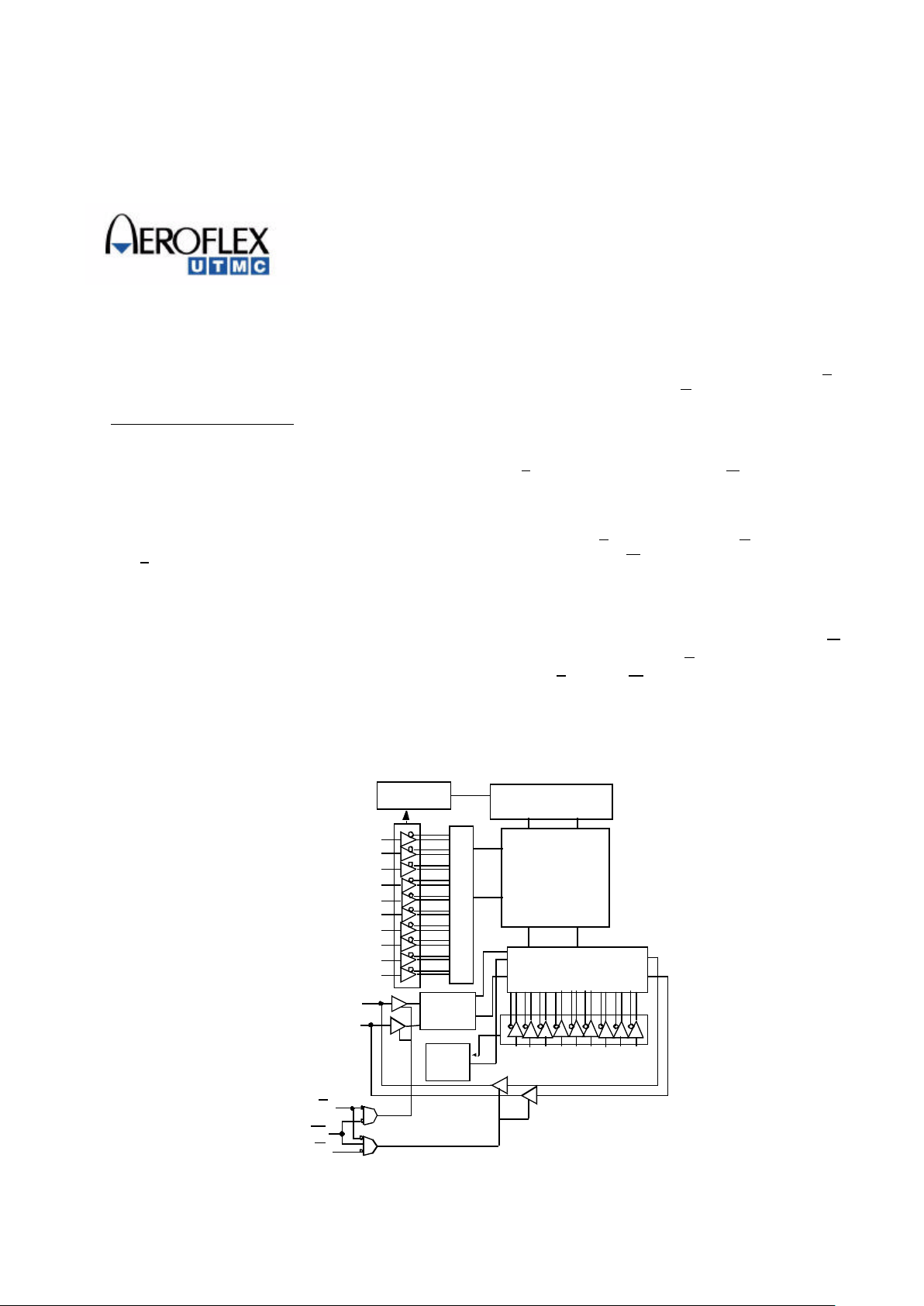
Memory Array
1024 Rows
512x8 Columns
Pre-Charge Circuit
Clk. Gen.
Row Select
A0
A1
A2
A3
A4
A5
A6
A7
A8
A9
I/O Circuit
Column Select
Data
Control
CLK
Gen.
A10
A11
A12
A13
A14
A15
A16
A17
A18
DQ 0 - DQ
7
W
G
E
Figure 1. UT9Q512 SRAM Block Diagram

2
PIN NAMES
DEVICE OPERATION
The UT 9Q512 has three control inputs called Enable 1 (E), Write
Enable (W), and Output Enable (G); 19 address inputs, A(18:0);
and eight bidirectional data lines, DQ(7:0). E Device Enable
controls device selection, active, and standby modes. Asserting
E enables the device, causes I
DD
to rise to its active value, and
decodes the 19 address inputs to select one of 524,288 words in
the memory. W controls read and write operations. During a
read cycle, G must be asserted to enable the outputs.
Table 1. Device Operation Truth Table
Notes:
1. “X” is defined as a “don’t care” condition.
2. Device active; outputs disabled.
READ CYCLE
A combination of W greater than V
IH
(min) and E less than V
IL
(max) defines a read cycle. Read access time is measured from
the latter of Device Enable, Output Enable, or valid address to
valid data output.
SRAM Read Cycle 1, the Address Access in figure 3a, is
initiated by a change in address inputs while the chip is enabled
with G asserted and W deasserted. Valid data appears on data
outputs DQ(7:0) after the specified t
AVQV
is satisfied. Outputs
remain active throughout the entire cycle. As long as Device
Enable and Output Enable are active, the address inputs may
change at a rate equal to the minimum read cycle time (t
AVAV
).
SRAM read Cycle 2, the Chip Enable - Controlled Access in
figure 3b, is initiated by E going active while G remains asserted,
W remains deasserted, and the addresses remain stable for the
entire cycle. After the specified t
ETQV
is satisfied, the eight-bit
word addressed by A(18:0) is accessed and appears at the data
outputs DQ(7:0).
SRAM read Cycle 3, the Output Enable - Controlled Access in
figure 3c, is initiated by G going active while E is asserted, W
is deasserted, and the addresses are stable. Read access time is
t
GLQV
unless t
AVQV
or t
ETQV
have not been satisfied.
A(18:0) Address
DQ(7:0) Data Input/Output
E Enable
W Write Enable
G Output Enable
V
DD
Power
V
SS
Ground
1 36
2 35
3 34
4 33
5 32
6 31
7 30
8 29
9 28
10 27
11 26
12 25
13 24
14 23
15 22
16 21
17 20
18 19
Figure 2. UT9Q512 25ns SRAM Pinout (36)
(For both shielded and unshielded packages)
NC
A18
A17
A16
A15
G
DQ7
DQ6
V
SS
V
DD
DQ5
DQ4
A14
A13
A12
A11
A10
NC
A0
A1
A2
A3
A4
E
DQ0
DQ1
V
DD
V
SS
DQ2
DQ3
W
A5
A6
A7
A8
A9
G W E I/O Mode Mode
X
1
X 1 3-state Standby
X 0 0 Data in Write
1 1 0 3-state
Read
2
0 1 0 Data out Read

3
WRITE CYCLE
A combination of W less than VIL(max) and E less than
VIL(max) defines a write cycle. The state of G is a “don’t care”
for a write cycle. The outputs are placed in the high-impedance
state when either G is greater than VIH(min), or when W is less
than VIL(max).
Write Cycle 1, the Write Enable - Controlled Access in figure
4a, is defined by a write terminated by W going high, with E
still active. The write pulse width is defined by t
WLWH
when the
write is initiated by W, and by t
ETWH
when the write is initiated
by E. Unless the outputs have been previously placed in the highimpedance state by G, the user must wait t
WLQZ
before applying
data to the nine bidirectional pins DQ(7:0) to avoid bus
contention.
Write Cycle 2, the Chip Enable - Controlled Access in figure
4b, is defined by a write terminated by E going inactive. The
write pulse width is defined by t
WLEF
when the write is initiated
by W, and by t
ETEF
when the write is initiated by the E going
active. For the W initiated write, unless the outputs have been
previously placed in the high-impedance state
by G, the user must wait t
WLQZ
before applying data to the eight
bidirectional pins DQ(7:0) to avoid bus contention.
TYPICAL RADIATION HARDNESS
Table 2. Radiation Hardness
Design Specifications
1
Notes:
1. The SRAM will not latchup during radiation exposure under recommended
operating conditions.
2. 10% worst case particle environment, Geosynchronous orbit, 0.025 mils of
Aluminum.
Total Dose 50 krad(Si)
Heavy Ion
Error Rate
2
<1E-8 Errors/Bit-Day

4
ABSOLUTE MAXIMUM RATINGS
1
(Referenced to VSS)
Notes:
1. Stresses outside the listed absolute maximum ratings may cause permanent damage to the device. This is a stress rating only, and functional operation of the device
at these or any other conditions beyond limits indicated in the operational sections of this specification is not recommended. Exposure to absolute maximum rating
conditions for extended periods may affect device reliability and performance.
2. Maximum junction temperature may be increased to +175°C during burn-in and steady-static life.
3. Test per MIL-STD-883, Method 1012.
RECOMMENDED OPERATING CONDITIONS
SYMBOL PARAMETER LIMITS
V
DD
DC supply voltage -0.5 to 7.0V
V
I/O
Voltage on any pin -0.5 to 7.0V
T
STG
Storage temperature -65 to +150°C
P
D
Maximum power dissipation 1.0W
T
J Maximum junction temperature
2
+150°C
Θ
JC
Thermal resistance, junction-to-case
3
10°C/W
I
I
DC input current
±10 mA
SYMBOL PARAMETER LIMITS
V
DD
Positive supply voltage 4.5 to 5.5V
T
C
Case temperature range (C) screening: -55° to +125°C
(E) screening: -40° to +125°C
V
IN
DC input voltage 0V to V
DD
5
DC ELECTRICAL CHARACTERISTICS (Pre/Post-Radiation)*
(-55°C to +125°C for (C) screening and -40oC to +125oC for (W) screening) (VDD = 5.0V + 10%)
Notes:
* Post-radiation performance guaranteed at 25°C per MIL-STD-883 Method 1019 .
1. Measured only for initial qualification and after process or design changes that could affect input/output capacitance.
2. Supplied as a design limit but not guaranteed or tested.
3. Not more than one output may be shorted at a time for maximum duration of one second.
SYMBOL PARAMETER CONDITION MIN MAX UNIT
V
IH
High-level input voltage 2.0 V
V
IL
Low-level input voltage 0.8 V
V
OL1
Low-level output voltage IOL = 8mA, VDD =4.5V
0.4
V
V
OL2
Low-level output voltage IOL = 200µA,VDD =4.5V 0.05 V
V
OH1
High-level output voltage IOH = -4mA,VDD =4.5V 2.4 V
V
OH2
High-level output voltage IOH = -200µA,VDD =4.5V 3.2 V
C
IN
1
Input capacitance ƒ = 1MHz @ 0V 10 pF
C
IO
1
Bidirectional I/O capacitance ƒ = 1MHz @ 0V 12 pF
I
IN
Input leakage current VIN = VDD and V
SS, VDD
= VDD (max) -2 2 µA
I
OZ
Three-state output leakage current VO = VDD and V
SS
VDD = VDD (max)
G = VDD (max)
-2 2 µA
I
OS
2, 3
Short-circuit output current VDD = VDD (max), VO = V
DD
VDD = VDD (max), VO = 0V
-90 90 mA
IDD(OP) Supply current operating
@ 1MHz
Inputs: VIL = 0.8V,
VIH = 2.0V
I
OUT
= 0mA
VDD = VDD (max)
125 mA
I
DD1
(OP) Supply current operating
@40MHz
Inputs: VIL = 0.8V,
VIH = 2.0V
I
OUT
= 0mA
VDD = VDD (max)
180 mA
I
DD2
(SB) Supply current standby
@0MHz
Inputs: VIL = VSS
I
OUT
= 0mA
E = V
DD
- 0.5
VDD = VDD (max)
VIH = VDD - 0.5V
6
6
12
mA
mA
mA
-55°C and 25°C
-40°C and 25°C
125°C
6
AC CHARACTERISTICS READ CYCLE (Pre/Post-Radiation)*
(-55°C to +125°C for (C) screening and -40oC to +125oC for (W) screening) (VDD = 5.0V + 10%)
Notes: * Post-radiation performance guaranteed at 25 °C per MIL-STD-883 Method 1019.
1. Functional test.
2. Three-state is defined as a 500mV change from steady-state output voltage (see Figure 3).
3. The ET (enable true) notation refers to the falling edge of E. SEU immunity does not affect the read parameters.
4. The EF (enable false) notation refers to the rising edge of E. SEU immunity does not affect the read parameters.
SYMBOL PARAMETER
MIN MAX
UNIT
t
AVAV
1
Read cycle time 20 ns
t
AVQV
Read access time 25 ns
t
AXQX
Output hold time 3 ns
t
GLQX
G-controlled Output Enable time 0 ns
t
GLQV
G-controlled Output Enable time (Read Cycle 3) 10 ns
t
GHQZ
2
G-controlled output three-state time 10 ns
t
ETQX
3
E-controlled Output Enable time 3 ns
t
ETQV
3
E-controlled access time 25 ns
t
EFQZ
1,2,4
E-controlled output three-state time 10 ns
{
{
}
}
V
LOAD
+ 500mV
V
LOAD
- 500mV
V
LOAD
VH - 500mV
VL + 500mV
Active to High Z LevelsHigh Z to Active Levels
Figure 3. 5-Volt SRAM Loading

7
Assumptions:
1. E and G < VIL (max) and W > VIH (min)
A(18:0)
DQ(7:0)
Figure 4a. SRAM Read Cycle 1: Address Access
t
AVAV
t
AVQV
t
AXQX
Previous Valid Data
Valid Data
Assumptions:
1. G < VIL (max) and W > VIH (min)
A(18:0)
Figure 4b. SRAM Read Cycle 2: Chip Enable-Controlled Access
E
DATA VALID
t
EFQZ
t
ETQV
t
ETQX
DQ(7:0)
Figure 4c. SRAM Read Cycle 3: Output Enable-Controlled Access
A(18:0)
DQ(7:0)
G
t
GHQZ
Assumptions:
1. E< VIL (max) and W > VIH (min)
t
GLQV
t
GLQX
t
AVQV
DATA VALID

8
AC CHARACTERISTICS WRITE CYCLE (Pre/Post-Radiation)*
(-55°C to +125°C for (C) screening and -40oC to +125oC for (E) screening) (VDD = 5.0V + 10%)
Notes:
* Post-radiation performance guaranteed at 25°C per MIL-STD-883 Method 1019.
1. Functional test performed with outputs disabled (G high).
2. Three-state is defined as 500mV change from steady-state output voltage (see Figure 3).
SYMBOL PARAMETER
9Q512-25
5.0V
MIN MAX
UNIT
t
AVAV
1
Write cycle time 20 ns
t
ETWH
Device Enable to end of write 20 ns
t
AVET
Address setup time for write (E - controlled) 0 ns
t
AVWL
Address setup time for write (W - controlled) 0 ns
t
WLWH
Write pulse width 20 ns
t
WHAX
Address hold time for write (W - controlled) 0 ns
t
EFAX
Address hold time for Device Enable (E - controlled) 0 ns
t
WLQZ
2
W - controlled three-state time 10 ns
t
WHQX
W - controlled Output Enable time 5 ns
t
ETEF
Device Enable pulse width (E - controlled) 20 ns
t
DVWH
Data setup time 15 ns
t
WHDX
Data hold time 2 ns
t
WLEF
Device Enable controlled write pulse width 20 ns
t
DVEF
Data setup time 15 ns
t
EFDX
Data hold time 2 ns
t
AVWH
Address valid to end of write 20 ns
t
WHWL
1
Write disable time 5 ns

9
Assumptions:
1. G < VIL (max). If G > VIH (min) then Q( 7:0) will be
in three-state for the entire cycle.
2. G high for t
AVAV
cycle.
W
t
AVWL
Figure 5a. SRAM Write Cycle 1: Write Enable - Controlled Access
A(18:0)
Q(7:0)
E
t
AVAV
2
D(7:0)
APPLIED DATA
t
DVWH
t
WHDX
t
ETWH
t
WLWH
t
WHAX
t
WHQX
t
WLQZ
t
AVWH
t
WHWL

10
t
EFDX
Assumptions & Notes:
1. G < VIL (max). If G > VIH (min) then Q(7:0) will be in three-state for the entire cycle.
2. Either E scenario above can occur.
3. G high for t
AVAV
cycle.
A(18:0)
Figure 5b. SRAM Write Cycle 2: Chip Enable - Controlled Access
W
E
D(7:0)
APPLIED DATA
E
Q(7:0)
t
WLQZ
t
ETEF
t
WLEF
t
DVEF
t
AVAV
3
t
AVET
t
AVET
t
ETEF
t
EFAX
t
EFAX
or
Notes:
1. 50pF including scope probe and test socket capacitance.
2. Measurement of data output occurs at the low to high or high to low transition mid-point
(i.e., CMOS input = VDD/2).
90%
Figure 6. AC Test Loads and Input Waveforms
Input Pulses
10%
< 5ns < 5ns
V
LOAD
= 1.55V
300 ohms
50pF
CMOS
0.5V
VDD-0.05V
10%

11
DATA RETENTION CHARACTERISTICS (Pre/Post- Irradiation)
(1 Second Data Retention Test)
Notes:
1. E = V
DD
- .2V, all other inputs = VDR or VSS.
2. Data retention current (I
DDR
) Tc = 25oC.
3. Not guaranteed or tested.
DATA RETENTION CHARACTERISTICS (Pre/Post-Irradiation)
(10 Second Data Retention Test, Tc= -55oC to 125oCf or (C) screening and -40oC to +125oC for (E) screening )
Notes:
1. Performed at VDD (min) and VDD (max).
2. E = VSS, all other inputs = VDR or VSS.
3. Not guaranteed or tested.
SYMBOL PARAMETER MINIMUM MAXIMUM UNIT
V
DR
VDD for data retention 2.5 -- V
I
DDR
1,2
Data retention current -- 5.0 mA
t
EFR
1,3
Chip select to data retention time 0 ns
t
R
1,3
Operation recovery time t
AVAV
ns
SYMBOL PARAMETER MINIMUM MAXIMUM UNIT
V
DD
1
VDD for data retention 4.5 5.5 V
t
EFR
2, 3
Chip select to data retention time 0 ns
t
R
2, 3
Operation recovery time t
AVAV
ns
V
DD
DATA RETENTION MODE
t
R
50%
50%
VDR > 2.5V
Figure 7. Low VDD Data Retention Waveform
t
EFR
E

12
PACKAGING
Figure 8. 36-pin Ceramic FLATPACK
1. All exposed metalized areas are gold plated over electroplated nickel per MIL-PRF-38535.
2. The lid is electrically connected to VSS.
3. Lead finishes are in accordance to MIL-PRF-38535.
4. Lead position and coplanarity are not measured.
5. ID mark is vendor option.
6. Total weight is approx. 3.42g.

13
1. All package finishes are per MIL-PRF-38535.
2. Letter designations are for cross-reference to MIL-STD-1835.
3. All leads increase max. limit by 0.003 measured at the center of the flat, when lead finish A (solder) is applied.
4. Total weight is approx. 10.77 g.
5. X-rays are an ineffective test for shielded packages.
.
Figure 9. 36-lead flatpack shielded package

14
ORDERING INFORMATION
512K x 8 SRAM:
= 25ns access time, 5.0V operation
20 = 20ns access time, 5.0V operation
Package Type:
(I) = 36-lead flatpack shielded package (bottom brazed)
(U) = 36-lead flatpack package (bottom brazed)
Screening:
(C) = Military Temperature Range flow
(P) = Prototype flow
(W) = Extended Industrial Temperature Range Flow (-40oC to +125oC)
Lead Finish:
(A) = Hot solder dipped
(C) = Gold
(X) = Factory option (gold or solder)
Notes:
1. Lead finish (A,C, or X) must be specified.
2. If an “X” is specified when ordering, then the part marking will match the lead finish and will be either “A” (solder) or “C” (gold).
3. Prototype flow per UTMC Manufacturing Flows Document. Tested at 25°C only. Lead finish is GOLD ONLY. Radiation neither
tested nor guaranteed.
4. Military Temperature Range flow per UTMC Manufacturing Flows Document. Devices are tested at -55°C, room temp, and +125°C.
Radiation neither tested nor guaranteed.
5. 36LBBFP Shielded Package for reduced high rel orders only.
6. Extended Industrial Temperature Range flow per UTMC Manufacturing Flows Document. Devices are tested at -40°C to +125°C.
Radiation neither tested nor guaranteed.
UT9Q512 - * * * *
-Aeroflex UTMC Core Part Number

15
512K x 8 SRAM: SMD
5962 - 00536
Lead Finish:
(A) = Hot solder dipped
(C) = Gold
(X) = Factory Option (gold or solder)
Case Outline:
(X) = 36-lead flatpack shielded package (bottom brazed)
(U) = 36-lead ceramic flatpack (b ottom-brazed)
Class Designator:
(T) = QML Class T
(Q) = QML Class Q
Device Type
01 = 25ns access time, 5.0V operation, Mil-Temp
02 = 25ns access time, 5.0V operation, Extended Industrial Temp (-40oC to +125oC)
03 = 20ns access time, 5.0V operation, Mil-Temp
04 = 20ns access time, 5.0V operation, Extended Industrial Temp (-40oC to +125oC)
Drawing Number: 00536
Total Dose:
(D) = 1E4 (10 kr ad)(Si))
(P) = 3E4 (30 krad)(Si)), Contact Factory
(L) = 5E4 (50krad(Si)), Contact Factory
Federal Stock Class Designator: No options
* * ***
Notes:
1.Lead finish (A,C, or X) must be specified.
2.If an “X” is specified when ordering, part marking will match the lead finish and will be either “A” (solder) or “C” (gold).
3.Total dose radiation must be specified when ordering.
 Loading...