

UTC LP2950/2951 LINEAR INTEGRATED CIRCUIT
UTC UNISONIC TECHNOLOGIES CO., LTD. 1
QW-R102-001,E
100 mA LOW-DROPOUT VOLTAGE
REGULATOR
DESCRIPTION
The UTC LP2950/2951 is a monolithic integrated voltage
regulator with low dropout voltage, and low quiescent current.
It includes many features that suitable for different
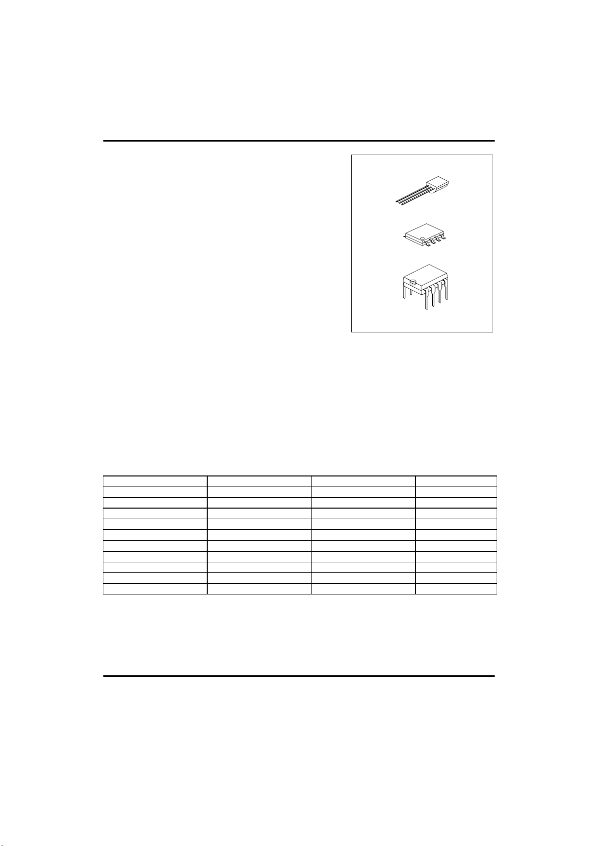
applications. Available in 3-pin TO-92, DIP-8 and SOP-8
packages.
FEATURES
*High accuracy 2.5, 3.0, 3.3, 3.6 or 5V fixed output for
TO-92, SOP-8 package.
*Extremely low quiescent current and dropout voltage.
*Extremely tight load and line regulation.
*Current and thermal limiting.
*Very low temperature coefficient.
*Logic controlled shutdown and error flag available for DIP
and SOP package.
*Output voltage programmable for DIP and SOP package.
APPLICATIONS
*Battery powered equipment.
*High efficient linear regulator down to 1.24V.
*Cellular phones.
TO-92
SOP-8
DIP-8
1
ORDERING INFORMATION
PART NUMBER TEMPERATURE RANGE PACKAGE ACCURACY
UTC LP2950-5.0
-40 ~ +125°C
3-Pin TO-92 plastic 2.0%
UTC LP2950-3.0
-40 ~ +125°C
3-Pin TO-92 plastic 1.0%
UTC LP2950-3.3
-40 ~ +125°C
3-Pin TO-92 plastic 1.0%
UTC LP2950-3.6
-40 ~ +125°C
3-Pin TO-92 plastic 2.0%
UTC LP2950-2.5
-40 ~ +125°C
3-Pin TO-92 plastic 1.0%
UTC LP2950-5.0
-40 ~ +125°C
8-Pin SOP-8 plastic 2.0%
UTC LP2950-3.0
-40 ~ +125°C
8-Pin SOP-8 plastic 1.0%
UTC LP2950-3.3
-40 ~ +125°C
8-Pin SOP-8 plastic 1.0%
UTC LP2951
-40 ~ +125°C
8-Pin SOP-8 plastic 2.0%
UTC LP2951
-40 ~ +125°C
8-Pin DIP-8 plastic 2.0%
UTC LP2950/2951 LINEAR INTEGRATED CIRCUIT
UTC UNISONIC TECHNOLOGIES CO., LTD. 2
QW-R102-001,E
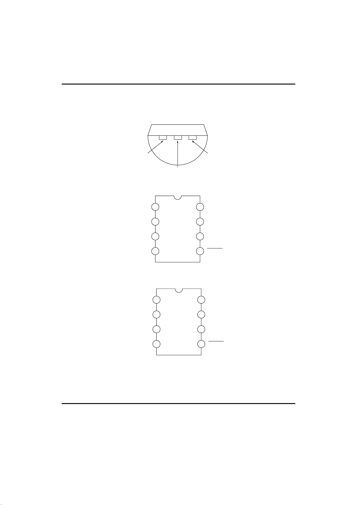
PIN CONFIGURATIONS
21 3
OUTPUT
GND
INPUT
UTC LP2950
TO-92 Plastic Package
Bottom View
1
2
3
4
8
7
6
5
INPUT
FEEDBACK
5V TAPSHUTDOW N
SENSE
OUTPUT
UTC
LP2951
GND
ERROR
SOP-8 OR DIP-8 PACKAGE
FOR UTC LP2951
1
2
3
4
8
7
6
5
INPUT
NC
NCSHUTDOWN
NC
OUTPUT
UTC
LP2950
GND
ERROR
SOP-8 OR DIP-8 PACKAGE
FOR UTC LP2950
Fig.1
UTC LP2950/2951 LINEAR INTEGRATED CIRCUIT
UTC UNISONIC TECHNOLOGIES CO., LTD. 3
QW-R102-001,E
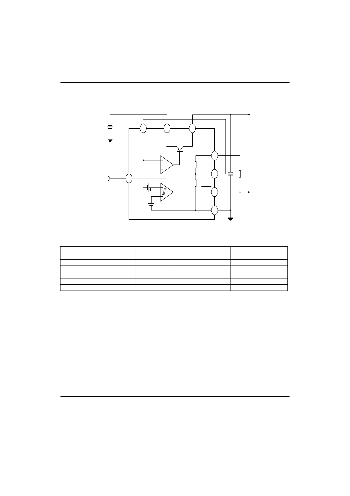
BLOCK DIAGRAM
5
4
6
2
187
3
60mV
330K
Ω
TO CMOS
OR TTL
5V 150mA
MAX.
FEEDBACK INPUT OUTPUT
SENSE
5V TAP
GND
ERROR
DETECTION
COMPARATOR
ERROR
AMPLIFIER
FROM CMOS
OR TTL
1.23
REF
SHUT
DOWN
UNRAGULATED
DC
ERROR
182k
Ω
60k
Ω
1.5 µF
FOR UTC LP2951
ABSOLUTE MAXIMUM RATINGS
PARAMETER
SYMBOL VALUE UNIT
Supply Voltage Vcc -0.3~+18 V
Feedback Voltage Vfeedback -1.5~+18 V
Shutdown Voltage Vshutdown -0.3~+18 V
Comparator Output Voltage Vco -0.3~+18 V
Storage Temperature Tstr -65~+150
°C
Operating Junction Temperature Tj -40~+125
°C

UTC LP2950/2951 LINEAR INTEGRATED CIRCUIT
UTC UNISONIC TECHNOLOGIES CO., LTD. 4
QW-R102-001,E
ELECTRICAL CHARACTERISTICS
(Tested at Tj=25°C,V
IN=6V,IL=100µA and CL=1µF, unless otherwise specified)
PARAMETER PART NUMBER TEST CONDITION
MIN. TYP. MAX.
UNIT
Output Voltage UTC LP2950-2.5
UTC LP2950-3.0
UTC LP2950-3.3
UTC LP2950-3.6
UTC LP2950-5.0
UTC LP2951
T
J=25°C
(note 1)
2.47
2.97
3.27
3.53
4.90
2.5
3.0
3.3
3.6
5.0
2.53
3.03
3.33
3.67
5.10
V
UTC LP2950-2.5
UTC LP2950-3.0
UTC LP2950-3.3
UTC LP2950-3.6
UTC LP2950-5.0
UTC LP2951
-25°C<=T
J<=<=+85°C
(note 1)
2.47
2.97
3.27
3.53
4.90
2.5
3.0
3.3
3.6
5.0
2.53
3.03
3.33
3.67
5.10
V
Output Voltage UTC LP2950-2.5
UTC LP2950-3.0
UTC LP2950-3.3
UTC LP2950-3.6
UTC LP2950-5.0
UTC LP2951
100µA<=I
L<=100 mA
Tj<=Tj(max)
(note 1)
2.47
2.97
3.27
3.53
4.90
2.5
3.0
3.3
3.6
5.0
2.53
3.03
3.33
3.67
5.10
V
Output Voltage
Temperature Coefficient
20 100
ppm/°C
Line Regulation 6V<=VIN<=18V 0.03 0.1 0.2 %
Load Regulation
100µA<=I
L<=100 mA
0.04 0.1 0.2 %
Dropout Voltage
I
L=100µA
I
L=100mA (note 2)
50
380
80
450
150
600
mV
Ground Current
I
L=100µA
I
L=100mA
75
8
120
12
140
14
µA
mA
Dropout Ground Current
V
IN=4.5V,IL=100µA
110 170 200
µA
Current Limit Vout=0 160 200 220 mA
Output Noise 10Hz to
100KHz
C
L=1µF
C
L=200µF
C
L=3.3µF
(Bypass=0.01µF
pins 7 to (
utc2951))
430
160
100
µV
For LP2951 8-Pin version only
Reference Voltage 1.22 1.235 1.25 V
Reference Voltage (Note 4) 1.19 1.27 V
Feedback pin Bias
Current
20 40 nA
Reference Voltage
Temperature Coefficient
50
ppm/°C
Feedback Bias Current
temperature Coefficient
0.1
nA/°C

UTC LP2950/2951 LINEAR INTEGRATED CIRCUIT
UTC UNISONIC TECHNOLOGIES CO., LTD. 5
QW-R102-001,E
PARAMETER PART NUMBER TEST CONDITION
MIN. TYP. MAX.
UNIT
Error Comparator
Output Leakage Current VOH=18V 1
µA
Output Low Voltage VIN=4.5V
I
OL=400µA
250 mV
Upper Threshold
Voltage
(Note 3) 3.2 %VO
Lower Threshold
Voltage
(Note 3) 7.6 %VO
Hysteresis (Note 3) 15 mV
Shutdown Input
Input Logic Voltage
Low(Regulator ON)
High(Regulator OFF)
2.0
1.3
0.70
V
Shutdown Pin Input
Current
Vshutdown=2.4V
30 50
µA
Vshutdown=18V 450 600
µA
Regulator Output
Current Shutdown
Vshutdown>=2V,VIN<=18V,
V
out=0,
Feedback pin tied to 5V Tap.
3 10
µA
Note 1: Additional conditions for 8-pin versions are feedback tied to 5V Tap an Output tied to Output Sense
(V
out=5V) and Vshutdown<=0.8V.
Note 2:Dropout Voltage is defined as the input to output differential at which the output voltage drops 100mV
below its nominal value measured at 1V differential.
Note 3:Comparator thresholds are expressed in terms of percentage value of voltage output.
Note 4:Vref≤Vout≤(Vin-1V), 2.3V≤Vin≤30V, 100µA≤I
L
≤100mA, TJ≤T
JMAX

UTC LP2950/2951 LINEAR INTEGRATED CIRCUIT
UTC UNISONIC TECHNOLOGIES CO., LTD. 6
QW-R102-001,E
APPLICATION CIRCUIT
(10 Ampere Low Dropout Regulator)
+V
IN
FB
Vout
GND
SD
ERROR
UTC LP2951
8
5
7
14
3
CURRENT
LIMIT
SECTION
+V
IN=Vou
t+0.5V
0.05Ω
470
Ω
680
Ω
4.7M
Ω
20k
Ω
220
Ω
0.033µF
47
Ω
R1
R2
4.7
µ
F
100
µ
F
1%
10k
Ω
2N3906
+
V
OUT
100m A
Vout=1.23V*(1+R1/R2)
For 5V output
use internal resistors.Wire pin 6 to 7
and wire pin 2 to +V
out
UTC
D65H0
Fig.2
UTC LP2950-2.5
UTC LP2950-3.0
UTC LP2950-3.3
UTC LP2950-3.6
UTC LP2950-5.0
Vin Vout
Fig.3

UTC LP2950/2951 LINEAR INTEGRATED CIRCUIT
UTC UNISONIC TECHNOLOGIES CO., LTD. 7
QW-R102-001,E
TYPICAL PERFORMANCE CHARACTERISTICS
1
2
34 560
0
1
2
3
4
5
6
Fig.4 Dropout Characteristics
INPUT VOLTAGE(V)
OUTPUT VOLTAGE(V)
RL=50k
Ω
RL=50
Ω
0 1 2 3 4 5 6 7 8 9 10 11 12
0
10
20
30
40
50
60
70
80
90
100
120
110
130
140
150
Fig.5 Input Current
INPUT CURRENT(mA)
INPUT VOLTAGE(V)
RL=50Ω
50
60
70
80
90
100
110
120
-75 -50 -25 0 25 50 75 100 125 150
Fig. 7 Ground Pin Current
QUIESCENT CURRENT( m A)
TEMPERATURE(°C)?
VIN=6V
I
L
=100µA
-75 -50 -25 0 25 50 75 100 125 150
4
5
6
7
8
TEMPERATURE(°C)?
Fig. 8 Ground Pin Current
QUIESCENT CURRENT(mA)
V IN=6V
I
L
=100mA
-75 -50 -25 0 25 50 75 100 125 150
100
110
120
130
140
150
160
170
TEMPERATURE(°C)?
SHORT CIRCUIT CURRENT(mA)
Fig. 10 Short Circuit Current
-75 -50 -25 0 25 50 75 100 125 150
0
50
100
300
400
500
600
>
TEMPERATURE(°C)?
DROPOUT VOLTAGE(mV)
Fig. 6 Dropout Voltage
IL=100mA
IL=100µA
-75 -50 -25 0 25 50 75 100 125 150
TEMPERATURE(°C)
0.6
0.8
1.0
1.2
1.4
1.6
1.8
Fig. 9 Shutdown Threshold Voltage
Shutdown Threshold Voltage(V)
0.1 1
10
100
0
100
200
300
400
500
Fig. 11 Dropout Voltage
OUTPUT CURRENT(mA)
Dropout Voltage(mV)
 Loading...