

UNISONIC TECHNOLOGIES CO., LTD
UC3863
LINEAR INTEGRATED CIRCUIT
LOW COST POWER-SAVING
MODE PWM CONTROLLER
FOR FLYBACK CONVERTERS
DESCRIPTION
The UC3863 is a high performance current mode PWM
controller ideally suited for low standby power. The PWM switching
frequency is programmable externally at normal operation. Low
V
startup current make the power reliable on startup design and
DD
a large value resistor could be used in the startup circuit to
minimize the standby power. At no load condition, the IC operates
in power-saving mode for lower standby power, decreasing
frequency for Higher conversion efficiency at light load condition.
The UC3863 contains protection with automatic recovery
including OLP (over load protection), OTP (over temperature
protection), OVP (over voltage protection), UVLO (V
clamp and under voltage lockout).To protect the power MOSFET,
Gate-drive output is fixed up to 15V max. The UC3863 contains
protection OCP (cycle-by-cycle current limiting).
The internal slope compensation improves system stability at
high PWM duty cycle output. Leading-edge blanking on current
sense input removes the signal glitch, which offering minimal
external component count in the design. Excellent EMI
performance is achieved with UTC proprietary frequency hopping
technique (ZL201020615247.1) together with soft driver control.
Audio noise is eliminated due to switch frequency more than 20kHz
during operation.
The UC3863 has such applications as: battery charger, power
adaptor, set-top box power supplies, ink jet printers, open-frame
SMPS
over voltage
DD
FEATURES
* UTC proprietary frequency hopping technology for Improved EMI
performance.
* Power-saving mode for high light-load and standby efficiency
* Dynamic peak current limiting for constant output power
* Built-in synchronized slope compensation
* OTP,OLP,OVP and V
* Programmable PWM Frequency
* Gate output voltage clamped at 15V
* Low start-up current
* Cycle-by-cycle Current Limiting
* Under voltage lockout (UVLO)
* Few external components required
www.unisonic.com.tw 1 of 11
Copyright © 2013 Unisonic Technologies Co., Ltd QW-R103-058, B
clamp for higher security
DD
UC3863 LINEAR INTEGRATED CIRCUIT
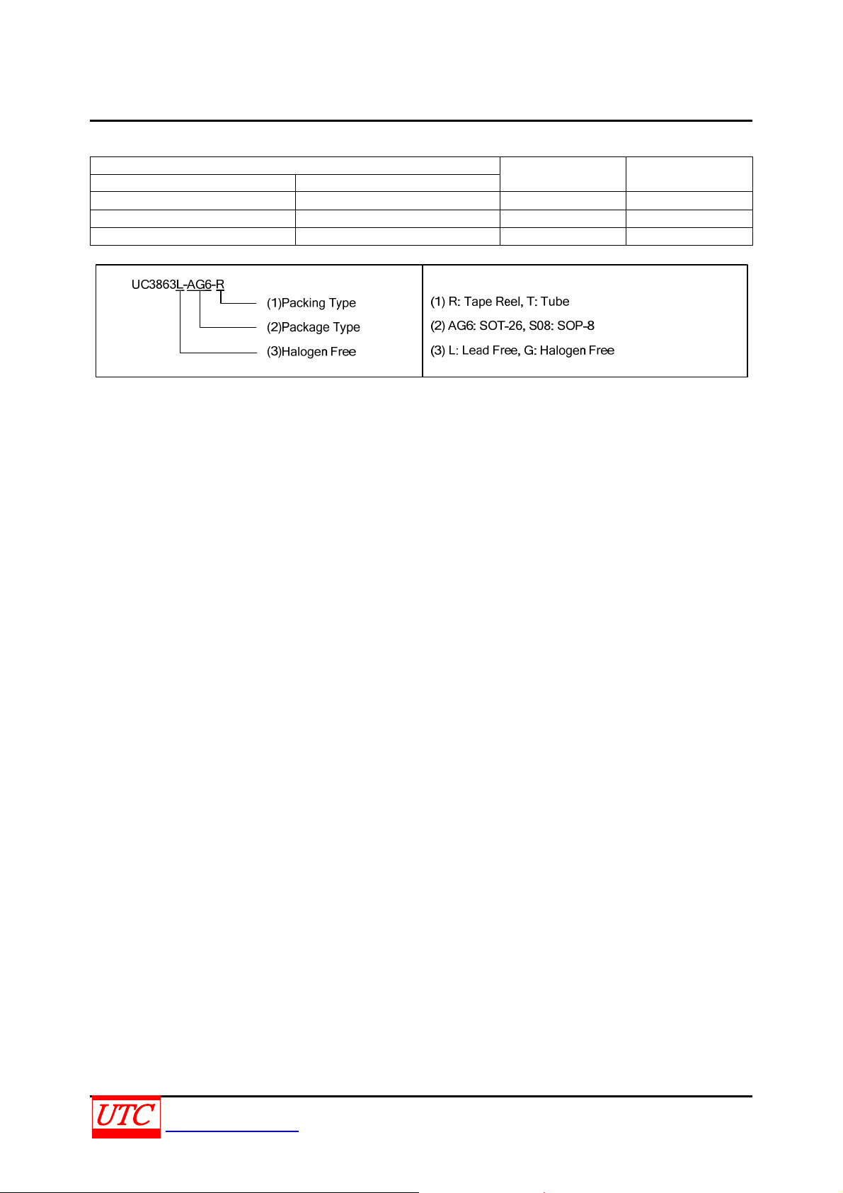
ORDERING INFORMATION
Ordering Number
Lead Free Halogen Free
UC3863L-AG6-R UC3863G-AG6-R SOT-26 Tape Reel
UC3863L-S08-T UC3863G-S08-T SOP-8 Tube
UC3863L-S08-R UC3863G-S08-R SOP-8 Tape Reel
Note: xx: Output Voltage, refer to Marking Information.
Package Packing
UNISONIC TECHNOLOGIES CO., LTD 2 of 11
www.unisonic.com.tw QW-R103-058, B

UC3863 LINEAR INTEGRATED CIRCUIT
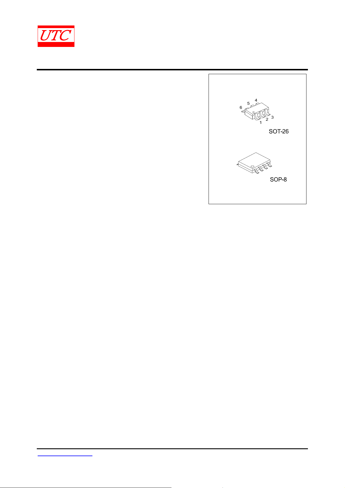
MARKING INFORMATION(For SOT-26)
PIN CONFIGURATION
SOT-26 SOP-8
PIN DESCRIPTION
PIN NO.
SOT-26 SOP-8
1 8 GND P Ground.
2 7 FB I
3 5 RI I
4 4 SENSE I
5 2 VDD P Power supply.
6 1 GATE O The totem-pole output driver for driving the power MOSFET.
- 3, 6 NC - No Connection
PIN NAME PIN TYPE DESCRIPTION
Feedback input pin. The PWM duty cycle is determined by
voltage level into this pin and SENSE pin input.
A resistor connected between RI and GND sets switching
frequency. A 100kΩ resistor RI results in a 65KHz switching
frequency.
Current sense input pin. Connected to MOSFET current sensing
resistor node.
UNISONIC TECHNOLOGIES CO., LTD 3 of 11
www.unisonic.com.tw QW-R103-058, B
UC3863 LINEAR INTEGRATED CIRCUIT
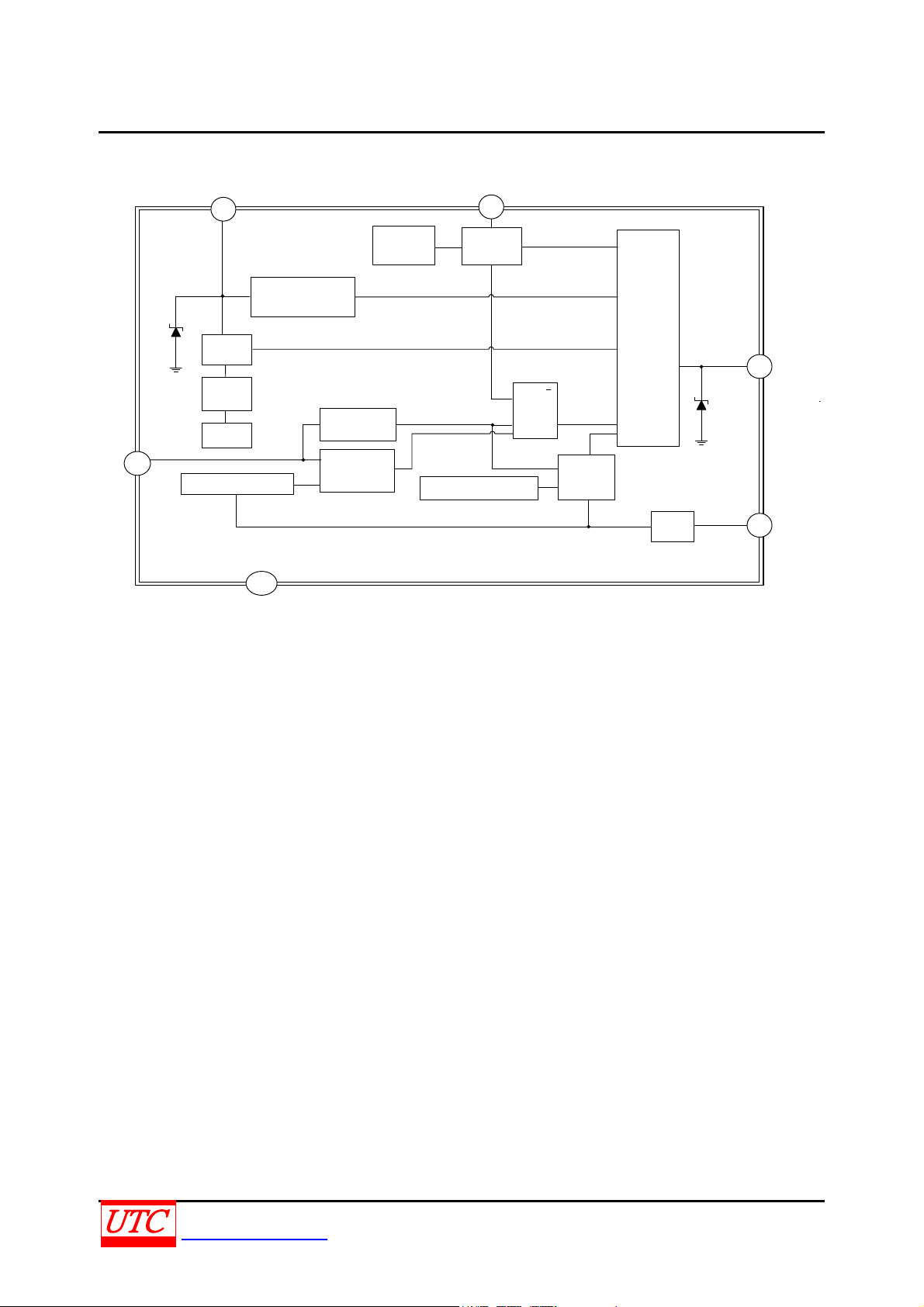
BLOCK DIAGRAM
V
5/2
DD
RI
3/5
FB
2/7
Reference voltage
OVP
Logic
Control
OTP
Slope Compensation
1/8
GND
UVLO
Frequency
Burstmode
PWM COMP
Hopping
Constant Power Limit
Oscillator
Latch
S
R
Driver
6/1
GATE
Q
Q
OCP
4/4
LEB
SENSE
UNISONIC TECHNOLOGIES CO., LTD 4 of 11
www.unisonic.com.tw QW-R103-058, B

UC3863 LINEAR INTEGRATED CIRCUIT
)
)
)
)
)
)
)
y
(
)
ABSOLUTE MAXIMUM RATINGS (T
=25°C, VDD =15V, unless otherwise specified)
A
PARAMETER SYMBOL RATINGS UNIT
Supply Voltage VDD 30 V
Input Voltage to FB Pin VFB -0.3 ~ 7 V
Input Voltage to CS Pin V
-0.3 ~ 7 V
SENSE
Junction Temperature TJ +150 °C
Operating Temperature T
Storage Temperature T
-40 ~ +125 °C
OPR
STG
-50 ~ +150 °C
Note: Absolute maximum ratings are those values beyond which the device could be permanently damaged.
Absolute maximum ratings are stress ratings only and functional device operation is not implied.
OPERATING RANGE
PARAMETER SYMBOL RATINGS UNIT
Supply Voltage VDD 10 ~ 26 V
ELECTRICAL CHARACTERISTICS (T
PARAMETER SYMBOL TEST CONDITIONS MIN TYP MAX UNIT
SUPPLY SECTION
Start Up Current I
IC Operating current IOP VFB=3.5V 1.5 5 mA
VDD Zener Clamp current I
UNDER-VOLTAGE LOCKOUT SECTION
Start Threshold Voltage V
Min. Operating Voltage V
CONTROL SECTION
VFB Open Loop Voltage Level V
PWM Input Gain A
Burst-Mode Out FB Voltage V
Reduce-Frequency end FB Voltage V
Burst-Mode Enter FB Voltage V
Switch Frequency
Duty Cycle D
Frequency Hopping F
Frequency VDD Stability FDV VDD=12V~20V 5 %
Frequency Temperature Stability FDT T=-20~100°C 1.5 5 %
RI Resistor Value Range RI 50 100 150 KΩ
Feedback Resistor RFB 11 KΩ
PROTECTION SECTION
VCC Over Voltage Protection Threshold V
FB PIN Over Load Protection Threshold V
Over Load Protection Delay-Time T
OTP threshold T
CURRENT LIMITING SECTION
Peak Current Flat Threshold Voltage V
Peak Current Valley Threshold Voltage V
Lead Edge Blanking Time T
DRIVER OUTPUT SECTION
Output Voltage Low State VOL VDD=16,IO=-20mA 0.8 V
Output Voltage High State VOH VDD=16,IO= 20mA 11 V
Output Voltage Rise Time tR C
Output Voltage Fall Time tF C
Normal
Power-Saving Before enter burst mode 22 KHz
=25°C, VDD=15V, RI =100KΩ,unless otherwise specified)
A
VDD= V
STR
VDD>V
CLAMP
13 14 15 V
THD(ON
7.5 12 V
DD(MIN
5 V
FB-OPEN
ΔVFB/ΔV
VCS
V
FB(OUT
FB(END
FB(IN
FSW
VFB=3.5V, V
MAX
J(SW
VFB=4.2V 26 V
OVP
4.7 4.5 5.2 V
OLP
55 mS
Dela
VFB=4.2V 135 °C
THR
VFB=4.2V, Duty≥60% 0.6 0.65 0.7 V
CS-F
VFB=4.2V, Duty=0% 0.6 0.65 0.7 V
CS-V
400 ns
LEB
SENSE
V
SENSE
V
SENSE
=3.5V, RI=100KΩ 60 65 70 KHz
V
FB
-4 +4 %
=1.0nF 100 ns
L
=1.0nF 60 ns
L
-0.1V 5 20 μA
DD(ON
15 mA
OVP
CS
3 V/V
=0 1.1 V
=0 1.8 V
=0 0.9 V
=0 75 %
SENSE
UNISONIC TECHNOLOGIES CO., LTD 5 of 11
www.unisonic.com.tw QW-R103-058, B

UC3863 LINEAR INTEGRATED CIRCUIT
OPERATION DESCRIPTION
The UC3863 devices integrate many useful designs into one controller for low-power switch-mode power
supplies. The following descriptions highlight some of the features of the UC3863 series.
Start-up Current
The start-up current is only 5μA. Low start-up current allows a start-up resistor with a high resistance and a
low-wattage to supply the start-up power for the controller. For AC/DC adaptor with universal input range design, a
2.5~3MΩ, 1/8W startup resistor could be used together with a V
dissipation solution.
Power-Saving Mode Operation
The proprietary Power-Saving Mode function provides linearly decreasing the switching frequency under
light-load conditions for higher efficiency. The feedback voltage, which is sampled from the voltage feedback loop, is
taken as the reference. Once the feedback voltage dropped below the threshold voltage, the switching frequency
starts to decrease. This Power-Saving Mode function dramatically reduces power consumption under light-load
conditions. The 22KHz minimum frequency control also eliminates the audio noise at any loading conditions.
At zero load condition, the magnitude of power loss is in proportion to the number of switching events within a
fixed period of time. Reducing switching events leads to the reduction on the power loss and thus conserves the
energy. The UC3863 enter burst mode at standby condition to minimize the switching loss and reduces the standby
power consumption. Power supplies using the UC3863 can easily meet even the strictest regulations regarding
standby power consumption.
Switch Frequency Set
The maximum switch frequency is set through the 100KΩ RI-pin resistor to 65KHz. Switch frequency is
modulated by output power P
during IC operating. At no load or light load condition, most of the power dissipation
OUT
in a switching mode power supply is from switching loss on the MOSFET transistor, the core loss of the transformer
and the loss on the snubber circuit. The magnitude of power loss is in proportion to the number of switching events
within a fixed period of time. So lower switch frequency at lower load, which more and more improve IC’s efficiency
at light load. At from no load to light load condition, The IC will operate at from Burst mode to Reducing Frequency
Mode. The relation curve between f
through the RI-pin resistor RI: F
and P
SW
=6500/RI (KΩ) KHz.
SW
OUT/POUT (MAX)
as followed Fig.1. The maximum switch frequency is set
capacitor to provide a fast startup and low power
DD
Fig.1 The relation curve between fSW and relative output power P
OUT
/ P
OUT (MAX)
UNISONIC TECHNOLOGIES CO., LTD 6 of 11
www.unisonic.com.tw QW-R103-058, B

UC3863 LINEAR INTEGRATED CIRCUIT
OPERATION DESCRIPTION (Cont.)
Frequency Hopping For EMI Improvement
The Frequency hopping is implemented in the IC; there are two oscillators built-in the IC. The first oscillator is to
set the normal switching frequency; the switching frequency is modulated with a period signal generated by the 2nd
oscillator. The relation between the first oscillator and the 2nd oscillator as followed Fig.2. So the tone energy is
evenly spread out, the spread spectrum minimizes the conduction band EMI and therefore eases the system design
in meeting stringent EMI requirement.
Fig.2 Frequency Hopping
Built-in Slope Compensation
Built-in slope compensation circuit greatly improves the close loop stability at CCM and prevents the
sub-harmonic oscillation.
Leading-Edge Blanking
Each time the power MOSFET is switched on, a turn-on spike will inevitably occur at the sense-resistor. To avoid
premature termination of the switching pulse, a 400ns leading-edge blanking time is built in. Conventional RC
filtering can therefore be omitted. During this blanking period, the current-limit comparator is disabled and it cannot
switch off the gate driver.
Constant Output Power Limit
When the SENSE voltage, across the sense resistor R
GATE drive will be turned off after a small propagation delay t
current proportional to t
V
. Higher input line voltage will result in a larger additional current and hence the output power limit is also higher
IN
/Lp. Since the propagation delay is nearly constant regardless of the input line voltage
D×VIN
, reaches the threshold voltage, around 0.8V, the output
S
. This propagation delay will introduce an additional
D
than that under low input line voltage. To compensate this variation for wide AC input range, the threshold voltage is
adjusted by the V
higher line voltage will generate higher V
current. Since VIN pin is connected to the rectified input line voltage through a resistor R
IN
current into the VIN pin. The threshold voltage is decreased if the VIN
IN
VIN
, a
current is increased. Smaller threshold voltage, forces the output GATE drive to terminate earlier, thus reduce the
total PWM turn-on time and make the output power equal to that of low line input. This proprietary internal
compensation ensures a constant output power limit for wide AC input voltage from 90VAC to 264VAC.
Under Voltage Lockout (UVLO)
The turn-on and turn-off thresholds of the UC3863 are fixed internally at 15.8V/10V. During start-up, the hold-up
capacitor must be charged to 15.8V through the start-up resistor, so that the UC3863 will be enabled. The hold-up
capacitor will continue to supply V
V
must not drop below 10V during this start-up process. This UVLO hysteresis window ensures that hold-up
DD
capacitor will be adequate to supply V
until power can be delivered from the auxiliary winding of the main transformer.
DD
during start-up.
DD
Gate Output
The UC3863 output stage is a fast totem pole gate driver. Cross conduction has been avoided to minimize heat
dissipation, increase efficiency, and enhance reliability. A good tradeoff is achieved through dead time control. The
low idle loss and good EMI system design is easier to achieve with this dedicated control scheme. An internal 15V
clamp is added for MOSFET gate protection at higher than expected V
input.
DD
UNISONIC TECHNOLOGIES CO., LTD 7 of 11
www.unisonic.com.tw QW-R103-058, B

UC3863 LINEAR INTEGRATED CIRCUIT
OPERATION DESCRIPTION (Cont.)
Protection Controls
The IC takes on more protection functions such as OVP, OLP and OTP etc. In case of those failure modes for
continual blanking time, the driver is shut down. Driver is reset after failure is eliminated.
OVP
The OVP will shut down the switching of the power MOSFET whenever VDD >V
Fig.3.
Fig.3 OVP case Fig.4 OLP case
OLP
> V
OLP will shut down driver when V
OTP
OTP will shut down driver when junction temperature TJ>T
PCB Layout Note
Noise from the current sense or the control signal can cause significant pulse width jitter in
continuous-conduction mode, and slope compensation helps alleviate these problems. Good placement and layout
practices should be followed. Avoiding long PCB traces and component leads, locating compensation and filter
components near the UC3863, and increasing the power MOS gate resistance is advised.
FB
for continual a blanking time. The OLP event as followed Fig.4.
OLP
.
(THR)
. The OVP event as followed
OVP
UNISONIC TECHNOLOGIES CO., LTD 8 of 11
www.unisonic.com.tw QW-R103-058, B

UC3863 LINEAR INTEGRATED CIRCUIT
REFRENCE CIRCUIT (12V/1.5A)
BOM
Reference Component Reference Component
BD1 1N4007×4 L2 33μH 6*8mm
CX1 (Optional) NC Q1 4N65K
CY1 (Optional) YC 102P/400V (Y1) R1,R2 R 4.7MΩ 1206
C2 EC 33μF/400V 105°C R3 R 200K
C1 EC 6.8μF/400V 105°C R4 (Optional) 0Ω
C3 CC 0.001μF/1000V R5 R 24.9Ω
C4 EC 10μF/50V R6 R 42.21Ω 1206
C5,C13 (Optional) CC 104P/50V R7 R 0.66Ω 1W
C7 (Optional) NC R8 R 51kΩ 1206
C8 CC 103P/25V R9 R 100kΩ 0805
C9 NC R10 NC
C10 EC 470u/10V R12 R 220Ω 0805
C11 EC 220u/10V R13 R 1KΩ 0805
C12 CC 103P/50V 0805 R14 R 10KΩ 0805
C14 NC R15 R 100kΩ 0805
D2 Diode FR107 R16 R 25.94kΩ 0805
D4 (Optional) 1N4148 T1 EE-219
D5 MBR10100 U1
F1 2A/250V U2 TL431
L1 NC U3 PC817
IC UC3863
UNISONIC TECHNOLOGIES CO., LTD 9 of 11
www.unisonic.com.tw QW-R103-058, B

UC3863 LINEAR INTEGRATED CIRCUIT
TYPICAL CHARACTERISTICS
(V)
THD(ON)
V
(µA)
STR
I
(V)
DD(min)
V
(kHz)
SW
F
(KHz)
(%)
MAX
SW-Power-Saving
F
D
UNISONIC TECHNOLOGIES CO., LTD 10 of 11
www.unisonic.com.tw QW-R103-058, B

UC3863 LINEAR INTEGRATED CIRCUIT
TYPICAL CHARACTERISTICS (Cont.)
UTC assumes no responsibility for equipment failures that result from using products at values that
exceed, even momentarily, rated values (such as maximum ratings, operating condition ranges, or
other parameters) listed in products specifications of any and all UTC products described or contained
herein. UTC products are not designed for use in life support appliances, devices or systems where
malfunction of these products can be reasonably expected to result in personal injury. Reproduction in
whole or in part is prohibited without the prior written consent of the copyright owner. The information
presented in this document does not form part of any quotation or contract, is believed to be accurate
and reliable and may be changed without notice.
UNISONIC TECHNOLOGIES CO., LTD 11 of 11
www.unisonic.com.tw QW-R103-058, B

 Loading...