

UTC UB261G-AA-AG6-R, UB261G-AB-AG6-R, UB261G-AC-AG6-R, UB261G-AD-AG6-R, UB261G-AE-AG6-R Schematic [ru]
...
UNISONIC TECHNOLOGIES CO., LTD
UB261
Preliminary CMOS IC
1-CELL LITHIUM-ION/POLYMER
BATTERY PROTECTION IC
DESCRIPTION
The UTC UB261 is a series of lithium-ion/lithium-polymer
rechargeable battery protection ICs incorporating high accuracy
voltage detection circuits and delay circuits.
The UTC UB261 is suitable for protection of single cell lithium-ion /
lithium polymer battery packs from overcharge, over discharge and
over current.
The ultra-small package and less required external components
make it ideal to integrate the UTC UB261 into the limited space of
battery pack.
FEATURES
* Wide Supply Voltage Range: VDD=1.5V~8.0V
*
Ultra-Low Quiescent Current: I
*
Ultra-Low Power-Down Current: I
*
Overcharge Detection Voltage: V
*
Overcharge Release Voltage: V
*
Over Discharge Release Voltage: V
*
Over Discharge Release Voltage: V
*
Over Current 1 Detection Voltage: V
*
Over Current 2 Detection Voltage: V
*
Short Circuit Detection Voltage: V
*
Charger Detection Voltage: V
* Delay Times are Generated by an Internal Circuit. (External Capacitors are Unnecessary.)
=3.0A (VDD=3.5V)
OPE
=0.2A (VDD=1.5V)
PDN
=3.9V~4.4V
CU
=3.8V~4.4V
CL
=2.0V~3.0V
DL
=2.0V~3.4V
DU
=0.05V~0.30V
IOV1
=0.5V (Fixed)
IOV2
=1.2V (Fixed)
SHORT
=-0.7V (Fixed)
CHA
6
4
5
3
2
1
SOT-26
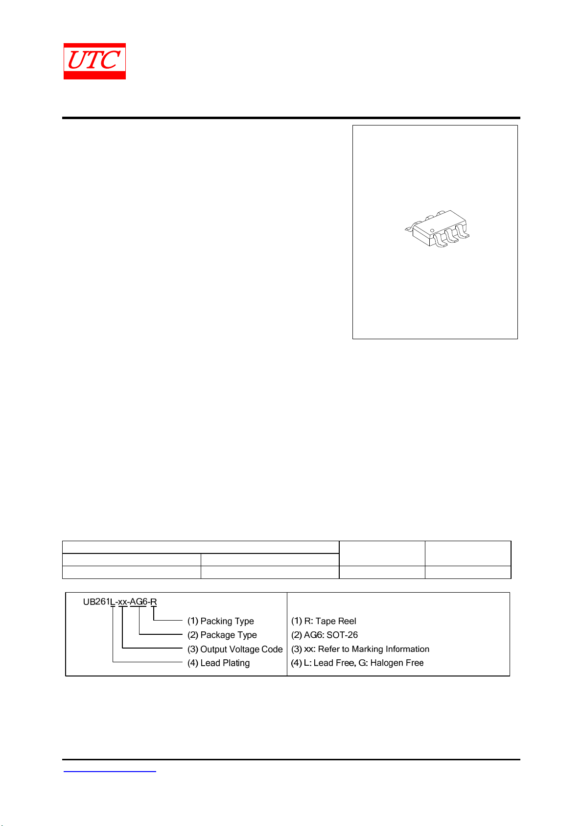
ORDERING INFORMATION
Ordering Number
Lead Free Halogen Free
UB261L-xx-AG6-R UB261G-xx-AG6-R SOT-26 Tape Reel
Note: xx: Output Voltage, refer to Marking Information.
www.unisonic.com.tw 1 of 10
Copyright © 2013 Unisonic Technologies Co., Ltd QW-R502 -A27.a
Package Packing
UB261 Preliminary CMOS IC
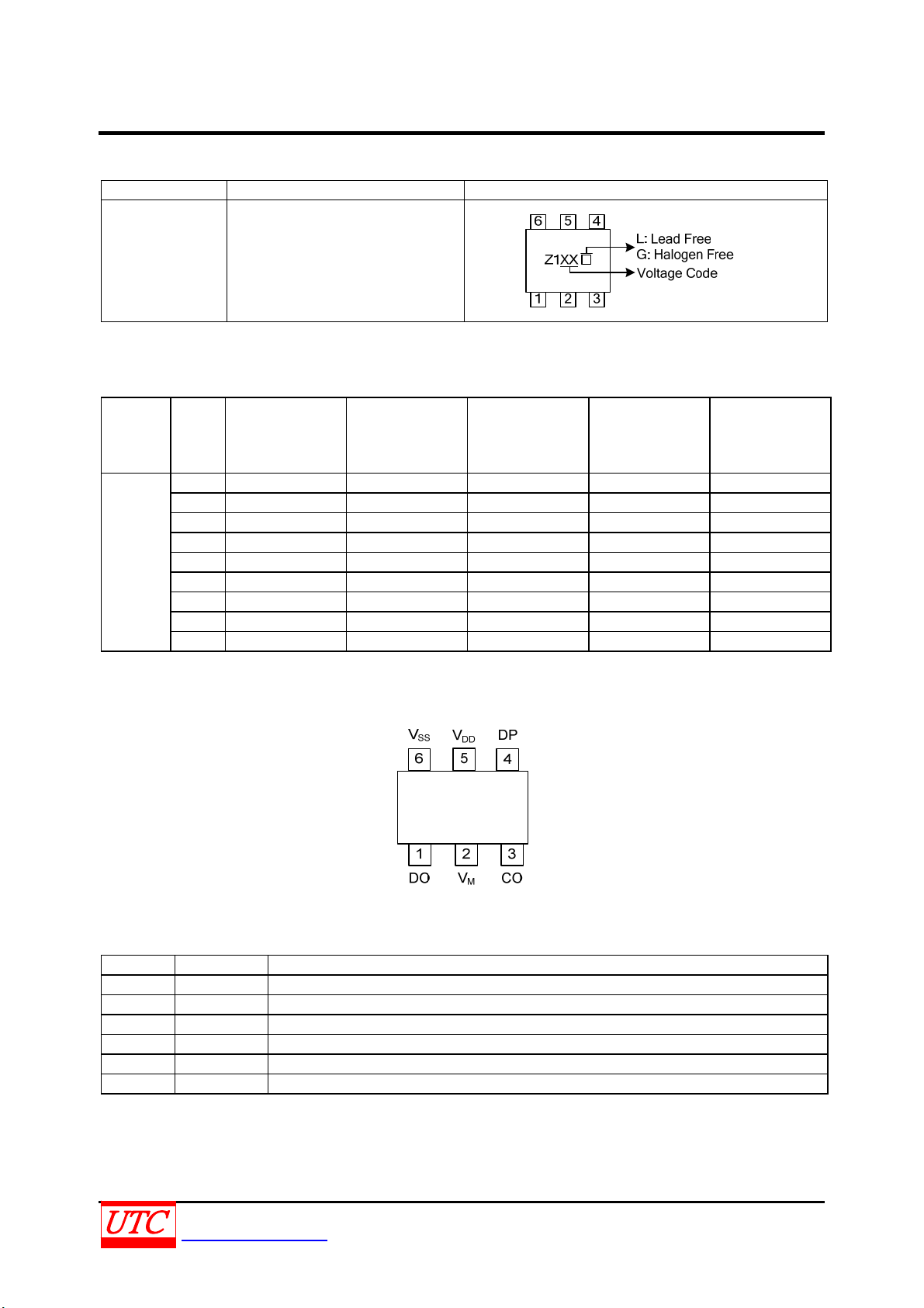
MARKING INFORMATION
PACKAGE VOLTAGE CODE (Note) MARKING
SOT-26
Note: Refer to Serial Code List
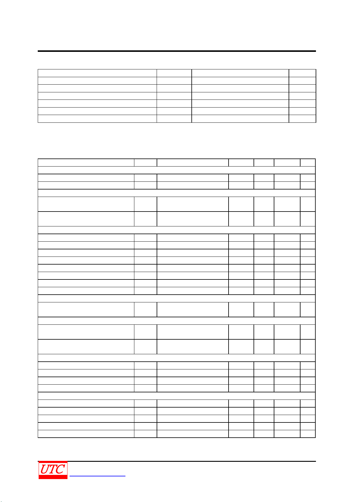
SERIAL CODE LIST
Overcharge
Model Code
AA 4.325 4.075 2.50 2.90 0.150
AB 4.325 4.075 2.50 2.90 0.100
AC 4.300 4.200 2.40 3.00 0.200
AD 4.280 4.180 2.50 3.00 0.150
UB261
AE 4.280 4.080 2.30 2.40 0.100
AF 4.275 4.075 2.50 2.90 0.150
AG 4.250 4.150 2.40 3.00 0.100
AH 4.200 4.100 2.80 2.90 0.150
AI 4.100 3.850 2.50 2.90 0.150
Detection
Voltage
[V
](V)
CU
PIN CONFIGURATION
XX
Overcharge
Release
Voltage
[V
](V)
CL
Over discharge
Detection
Voltage
[V
](V)
DL
Over discharge
Release
Voltage
[V
](V)
DU
Over Current
Detection
Voltage
[V
](V)
IOV1
PIN DESCRIPTION
PIN NO. PIN NAME DESCRIPTION
1 DO For discharge control: FET gate connection pin
2 VM For current sense and charger detection input pin
3 CO For charge control: FET gate connection pin
4 DP Test pin for delay time measurement
5 VDD Positive power input
6 VSS Negative power input
UNISONIC TECHNOLOGIES CO., LTD 2 of 10
www.unisonic.com.tw QW-R502-A27.a
UB261 Preliminary CMOS IC
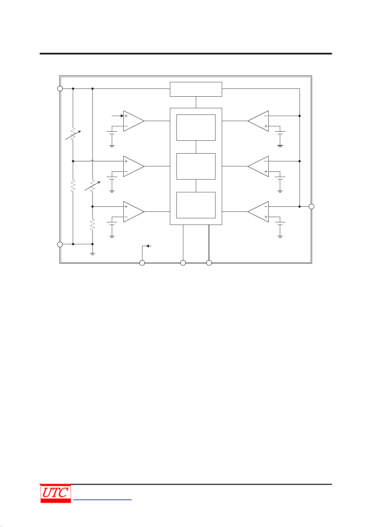
BLOCK DIAGRAM
V
DD
VM
Charger Detector
Overdischarge
Detector
Overcharge
Detector
V
SS
From Oscillator
0V Battery Charge
Inhibition Detector
Oscillator
Divider
Control
Logic
Short circuit Detector
Over current 2 Detector
Over current 1 Detector
V
M
DO
CODP
UNISONIC TECHNOLOGIES CO., LTD 3 of 10
www.unisonic.com.tw QW-R502-A27.a
UB261 Preliminary CMOS IC
ABSOLUTE MAXIMUM RATING (V
=0V, T
SS
=25° unless otherwise specified)
A
PARAMETER SYMBOL RATINGS UNIT
Input Voltage Between VDD and VSS (Note 2) VDD V
CO Output Pin Voltage VCO V
DO Output Pin Voltage VDO V
VM Input Pin Voltage VM V
Ambient Operating Temperature T
Storage Temperature T
-40 ~ +85 °
OPR
-55 ~ +125 °
STG
-0.3 ~ VSS+12 V
SS
-12 ~ VDD+0.3 V
DD
-0.3 ~ VDD+0.3 V
SS
-14 ~ VDD+0.3 V
DD
Notes: 1. Absolute maximum ratings are those values beyond which the device could be permanently damaged.
Absolute maximum ratings are stress ratings only and functional device operation is not implied.
2. Pulse (sec) noise exceeding the above input voltage (VSS+12V) may cause damage to the IC.
ELECTRICAL CHARACTERISTICS (V
=0V, TA=25° unless otherwise specified)
SS
PARAMETER SYMBOL TEST CONDITIONS MIN TYP MAX UNIT
CURRENT CONSOMPTION
Supply Current I
Power-Down Current I
VDD=3.5V, VM=0V 3.0 8.0 A
OPE
VDD=VM=1.5V 0.2 0.5 A
PDN
OPERATING VOLTAGE
Operating Voltage Between VDD-pin and
V
-pin
SS
Operating Voltage Between VDD-pin and
V
-pin
M
V
1.5 8 V
DS1
V
1.5 10 V
DS2
DETECTION VOLTAGE
Overcharge Detection Voltage VCU VCU-0.050 VCU VCU+0.050 V
Overcharge Release Voltage VCL VCL-0.050 VCL VCL+0.050 V
Overdischarge Detection Voltage VDL VDL-0.100 VDL VDL+0.100 V
Overdischarge Release Voltage VDU VDU-0.100 VDU VDU+0.100 V
Over Current 1 Detection Voltage V
Over Current 2 Detection Voltage V
Load Short Circuit Detection Voltage V
Charger Detection Voltage V
IOV1VDD
IOV2VDD
SHORT
CHA
=3.5V V
IOV1
-0.03 V
IOV1 VIOV1
+0.03 V
=3.5V 0.35 0.50 0.65 V
0.5 1.2 1.7 V
VDUVDL -1.6 -0.7 -0.2 V
0V BATTERY CHARGE VOLTAGE
0V Battery Charge Inhibition Battery
Voltage
V
0.9 1.8 V
0INH
INTERNAL RESISTANCE
Resistance between VM-pin and
V
-pin
DD
Resistance between VM-pin and
V
-pin
SS
R
VMDVDD
R
VMS
=1.8V, VM=0V 100 300 900 k
VDD=3.5V, VM=1.0V 10 30 70 k
OUTPUT RESISTANCE
CO-pin Resistance “H” R
CO-pin Resistance “L” R
DO-pin Resistance “H” R
DO-pin Resistance “L” R
COHVCO
COL
DOHVDO
DOL
=3.0V, VDD=3.5V, VM=0V 5 10 k
VCO=0.5V, VDD=4.5V, VM=0V 5 10 k
=3.0V, VDD=3.5V, VM=0V 5 10 k
VDO=0.5V, VDD=VM=1.8V 5 10 k
DELAY TIME
Overcharge Detection Delay Time tCU 0.9 1.2 1.5 s
Overdischarge Detection Delay Time tDL 110 150 190 ms
Over Current 1 Detection Delay Time t
Over Current 2 Detection Delay Time t
Short Circuit Detection Delay Time t
VDD=3.5V 6 9 12 ms
IOV1
VDD=3.5V 1 2.2 3.2 ms
IOV2
120 300 380 µs
SHORT
UNISONIC TECHNOLOGIES CO., LTD 4 of 10
www.unisonic.com.tw QW-R502-A27.a

UB261 Preliminary CMOS IC
OPERATION
1. Normal Condition
The UTC UB261 series monitors the voltage of the battery connected between V
voltage difference between VM pin and VSS pin to control charging and discharging. When the battery voltage is in
the range from the overdischarge detection voltage (V
voltage is in the range from the charger detection voltage (V
) to the overcharge detection voltage (VCU), and the VM pin
DL
) to the overcurrent 1 detection voltage (V
CHA
turns both the charging and discharging control FETs on. This condition is called the normal condition, and in this
condition charging and discharging can be carried out freely.
Note: When a battery is connected to the IC for the first time, discharging may not be enabled. In this case, short
the V
pin and VSS pin or connect the charger to restore the normal condition.
M
2. Overcurrent Condition
When a battery in the normal status is in the status where the voltage of the V
M
overcurrent detection voltage because the discharge current is higher than the specified value and the status lasts
for the overcurrent detection delay time, the discharge control FET is turned off and discharging is stopped. This
status is called the overcurrent status. In the overcurrent status, the V
between V
and VSS (R
M
) in the IC. However, the voltage of the VM pin is at the VDD potential due to the load as
VMS
long as the load is connected. When the load is disconnected, the V
and VSS pins are shorted by the resistor
M
pin returns to the VSS potential. This IC detects
M
the status when the impedance between the EB+ pin and EB- pin (Refer to the typical application circuit) increases
and is equal to the impedance that enables automatic restoration and the voltage at the V
detection voltage 1 (V
) or lower and the overcurrent status is restored to the normal status.
IOV1
Note: The impedance that enables automatic restoration varies depending on the battery voltage and the set value
of overcurrent 1 detection voltage.
3. Overcharge Condition
When the battery voltage becomes higher than the overcharge detection voltage (V
normal condition and the detection continues for the overcharge detection delay time (t
turns the charging control FET off to stop charging. This condition is called the overcharge condition. The overcharge
condition is released by the following two cases:
(1) When the battery voltage falls below the overcharge release voltage (V
), the UTC UB261 series turns the
CL
charging control FET on and turns to the normal condition.
(2) When a load is connected and discharging starts, the UTC UB261 series turns the charging control FET on
and returns to the normal condition. Just after the load is connected and discharging starts, the discharging current
flows through the parasitic diode in the charging control FET. At this moment the V
voltage for the parasitic diode, higher than V
voltage (V
) and provided that the V
CU
level. When the battery voltage goes under the overcharge detection
SS
pin voltage is higher than the overcurrent 1 detection voltage, the UTC
M
UB261 series releases the overcharge condition.
Note 1: If the battery is charged to a voltage higher than the overcharge detection voltage (V
voltage does not fall below the overcharge detection voltage (V
) even when a heavy load is connected, the
CU
detection of overcurrent 1, overcurrent 2 and load shortcircuiting do not function until the battery voltage falls below
over charge detection voltage (V
). Since an actual battery has an internal impedance of several dozens of m, the
CU
battery voltage drops immediately after a heavy load that causes overcurrent is connected, and the detection of
overcurrent 1, overcurrent 2 and load short-circuiting function.
Note 2: When a charger is connected after the overcharge detection, the overcharge condition is not released
even if the battery voltage is below the overcharge release voltage (V
the V
pin voltage goes over the charger detection voltage (V
M
CHA
). The overcharge condition is released when
CL
) by removing the charger.
pin and VSS pin and the
DD
), the IC
IOV1
pin is equal to or higher than the
pin returns to overcurrent
M
) during charging under the
CU
), the UTC UB261 series
CU
pin potential becomes Vf, the
M
) and the battery
CU
UNISONIC TECHNOLOGIES CO., LTD 5 of 10
www.unisonic.com.tw QW-R502-A27.a

UB261 Preliminary CMOS IC
OPERATION(Cont.)
4. Overdischarge Condition
When the battery voltage falls below the overdischarge detection voltage (VDL) during discharging under the
normal condition and the detection continues for the overdischarge detection delay time (t
turns the discharging control FET off to stop discharging. This condition is called the overdischarge condition. When
the discharging control FET is turned off, the V
(R
). When the voltage difference between the VM and VDD then is 1.2V (typ.) or lower, the current consumption is
VMD
reduced to the power-down current consumption (I
pin voltage is pulled up by the resistor between VM and VDD in the IC
M
). This condition is called the power-down condition.
PDN
The power-down condition is released when a charger is connected and the voltage difference between the V
and V
voltage (V
becomes 1.2V (typ.) or higher. Moreover when the battery voltage becomes the overdischarge detection
DD
) or higher, the UTC UB261 series turns the discharging FET on and returns to the normal condition.
DL
5. Charger Detection
When a battery in the overdischarge condition is connected to a charger and provided that the V
lower than the charger detection voltage (V
), the UTC UB261 series releases the overdischarge condition and
CHA
turns the discharging control FET on when the battery voltage becomes equal to or higher than the overdischarge
detection voltage (V
) since the charger detection function works. This action is called charger detection.
DL
When a battery in the overdischarge condition is connected to a charger and provided that the V
not lower than the charger detection voltage (V
), the UTC UB261 series releases the overdischarge condition
CHA
when the battery voltage reaches the overdischarge detection voltage (VDU) or higher.
6. Abnormal Charge Current Detection
If the VM pin voltage falls below the charger detection voltage (V
continues for the overcharge detection delay time (t
) , the charging control FET turns off and charging stops. This
CU
) during charging under normal condition and it
CHA
action is called the abnormal charge current detection.
Abnormal charge current detection works when the DO pin voltage is “H” and the V
charger detection voltage (V
). Consequently, if an abnormal charge current flows to an over-discharged battery,
CHA
the UTC UB261 series turns the charging control FET off and stops charging after the battery voltage becomes
higher than the overdischarge detection voltage which make the DO pin voltage “H”, and still after the overcharge
detection delay time (tCU) elapses.
Abnormal charge current detection is released when the voltage difference between V
less than charger detection voltage (V
CHA
).
7. Delay Circuits
The detection delay times are determined by dividing a clock of the approximately 3.5kHz with the counter.
Note 1: The detection delay time for overcurrent 2 (t
overcurrent 1 (V
detection delay time for each of them (= t
series turns the FET off within t
) is detected. When the overcurrent 2 (V
IOV1
or t
IOV2
or t
IOV2
SHORT
SHORT
of each detection.
) after the detection of overcurrent 1 (V
) and load short-circuiting (t
IOV2
) or load short-circuiting (V
IOV2
Note 2: When the overcurrent is detected and continues for longer than the overdischarge detection delay time (t
without releasing the load, the condition changes to the power-down condition when the battery voltage falls below
the overdischarge detection voltage (V
) due to the overcurrent, the UTC UB261 series turns the discharging control FET off by the overcurrent
(V
DL
). When the battery voltage falls below the overdischarge detection voltage
DL
detection. In this case the recovery of the battery voltage is so slow that if the battery voltage after the overdischarge
detection delay time (t
) is still lower than the over discharge detection voltage (V
DL
DL
to the power-down condition.
8. 0V Battery Charge Inhibiting Function
This function inhibits the recharging when a battery that is short-circuited (0V battery) internally is connected.
When the battery voltage is the 0V battery charge inhibition battery voltage (V
) or lower, the charging control FET
0INH
gate is fixed to EB- pin voltage to inhibit charging. When the battery voltage is the 0V battery charge inhibition
battery voltage (V
) or higher, charging can be performed.
0INH
), the UTC UB261 series
DL
M
pin voltage is
M
pin voltage is
M
pin voltage falls below the
M
pin and VSS pin becomes
M
) start when the
SHORT
) is detected over the
SHORT
), the UTC UB261
IOV1
DL
), the UTC UB261 series shifts
)
UNISONIC TECHNOLOGIES CO., LTD 6 of 10
www.unisonic.com.tw QW-R502-A27.a

UB261 Preliminary CMOS IC
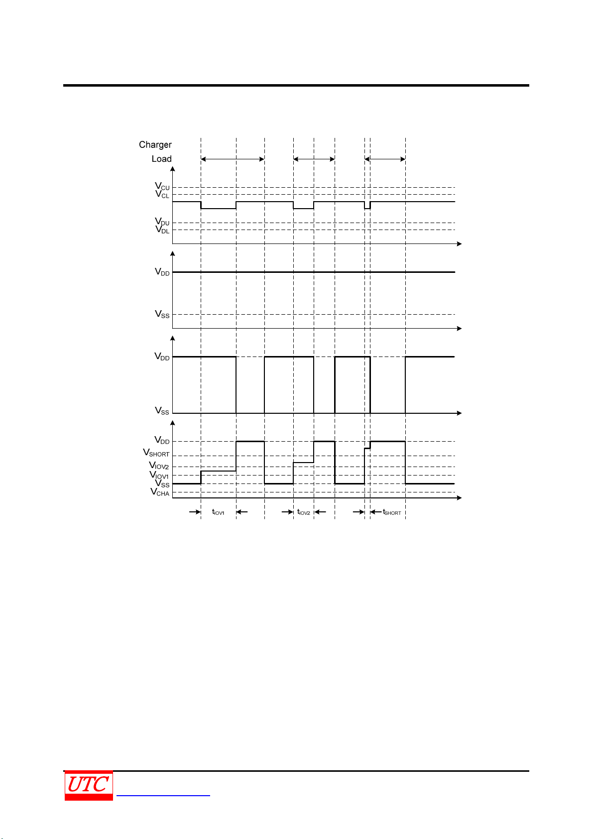
TIMING CHART
(1) Overcharge Detection, Overdischarge Detection
Battery Voltage
CO PinDO Pin
Pin
M
V
UNISONIC TECHNOLOGIES CO., LTD 7 of 10
www.unisonic.com.tw QW-R502-A27.a
UB261 Preliminary CMOS IC
TIMING CHART (Cont.)
(2) Discharge Overcurrent Detection
Battery Voltage
CO PinDO PinV
Pin
M
UNISONIC TECHNOLOGIES CO., LTD 8 of 10
www.unisonic.com.tw QW-R502-A27.a

UB261 Preliminary CMOS IC
TIMING CHART (Cont.)
(3) Abnormal Charge Overcurrent Detection
Battery Voltage
CO PinDO Pin
Pin
M
V
UNISONIC TECHNOLOGIES CO., LTD 9 of 10
www.unisonic.com.tw QW-R502-A27.a

UB261 Preliminary CMOS IC
TYPICAL APPLICATION CIRCUIT
EB+
Battery
R1=100~470
C1=0.1µF
V
DD
UTC UB261
V
SS
DO
M1 M2
CO
DP
V
M
R2=1k
EB-
Notes: 1. Overdischarge detection voltage must be higher than the threshold voltage of M1 and M2, if not, the M1
may not cut the charging current. If the threshold voltage of M1 equal to or higher than the overdischarge
detection voltage is used, discharging may be stopped before overdischarge is detected.
2. Charger voltage must be higher than the withstanding voltage between the gate and source of M1 and M2,
if not, M1 and M2 may be destroyed.
3. Resistance of R1 can’t be high, the value is about from 100 to 470, If R1 has a high resistance, the
voltage between V
pin and VSS pin may exceed the absolute maximum rating when a charger is
DD
connected in reverse since the current flows from the charger to the IC. Insert a resistor of 100 or higher
as R1 for ESD protection.
4. The capacitance of C1 must not be less than 0.022F, if not, DO pin may oscillate when load
short-circuiting is detected. Be sure to connect a capacitor of 0.022F or higher to C1, the typical value is
about 0.1F.
5. The resistance of R2 can not be higher than 2k, if not, the charging current may not be cut when a
high-voltage charger is connected.
UTC assumes no responsibility for equipment failures that result from using products at values that
exceed, even momentarily, rated values (such as maximum ratings, operating condition ranges, or
other parameters) listed in products specifications of any and all UTC products described or contained
herein. UTC products are not designed for use in life support appliances, devices or systems where
malfunction of these products can be reasonably expected to result in personal injury. Reproduction in
whole or in part is prohibited without the prior written consent of the copyright owner. The information
presented in this document does not form part of any quotation or contract, is believed to be accurate
and reliable and may be changed without notice.
UNISONIC TECHNOLOGIES CO., LTD 10 of 10
www.unisonic.com.tw QW-R502-A27.a

 Loading...