


UTC UB261G-AA-AG6-R, UB261G-AB-AG6-R, UB261G-AC-AG6-R, UB261G-AD-AG6-R, UB261G-AE-AG6-R Schematic [ru]
...
 UNISONIC TECHNOLOGIES CO., LTD
UB261 Preliminary CMOS IC
1-CELL LITHIUM-ION/POLYMER BATTERY PROTECTION IC
DESCRIPTION |
5 |
4 |
|
|
|
|
|
||
The UTC UB261 is a series of lithium-ion/lithium-polymer |
6 |
|
|
|
rechargeable battery protection ICs incorporating high accuracy |
|
|
|
2 3 |
|
|
|
||
voltage detection circuits and delay circuits. |
|
|
|
|
|
|
1 |
||
The UTC UB261 is suitable for protection of single cell lithium-ion / |
|
|
|
|
|
|
|
|
|
lithium polymer battery packs from overcharge, over discharge and |
|
|
|
SOT-26 |
over current. |
|
|
|
|
The ultra-small package and less required external components |
|
|
|
|
make it ideal to integrate the UTC UB261 into the limited space of |
|
|
|
|
battery pack. |
|
|
|
|
FEATURES
*Wide Supply Voltage Range: VDD=1.5V~8.0V
*Ultra-Low Quiescent Current: IOPE=3.0μA (VDD=3.5V)
*Ultra-Low Power-Down Current: IPDN=0.2μA (VDD=1.5V)
*Overcharge Detection Voltage: VCU=3.9V~4.4V
*Overcharge Release Voltage: VCL=3.8V~4.4V
*Over Discharge Release Voltage: VDL=2.0V~3.0V
*Over Discharge Release Voltage: VDU=2.0V~3.4V
*Over Current 1 Detection Voltage: VIOV1=0.05V~0.30V
*Over Current 2 Detection Voltage: VIOV2=0.5V (Fixed)
*Short Circuit Detection Voltage: VSHORT=1.2V (Fixed)
*Charger Detection Voltage: VCHA=-0.7V (Fixed)
*Delay Times are Generated by an Internal Circuit. (External Capacitors are Unnecessary.)
ORDERING INFORMATION
Ordering Number |
Package |
Packing |
||
Lead Free |
Halogen Free |
|||
|
|
|||
UB261L-xx-AG6-R |
UB261G-xx-AG6-R |
SOT-26 |
Tape Reel |
|
Note: xx: Output Voltage, refer to Marking Information.
www.unisonic.com.tw |
1 of 10 |
Copyright © 2013 Unisonic Technologies Co., Ltd |
QW-R502-A27.a |
UB261 |
Preliminary |
CMOS IC |
MARKING INFORMATION
PACKAGE |
VOLTAGE CODE (Note) |
|
|
|
|
|
|
|
|
|
|
|
|
MARKING |
|
SOT-26 |
XX |
|
|
|
|
|
|
|
|
|
|
|
|
|
|
|
|
|
|
|
|
|
|
|
|
|
|
|
|
||
|
|
|
|
|
|
|
|
|
|
|
|
|
|
||
|
|
|
|
|
|
|
|
|
|
|
|
|
|
||
|
|
|
|
|
|
|
|
|
|
|
|
|
|
|
|
|
|
|
|
|
|
|
|
|
|
|
|
|
|
|
|
|
|
|
|
|
|
|
|
|
|
|
|
|
|
|
|
Note: Refer to Serial Code List
SERIAL CODE LIST
|
|
Overcharge |
Overcharge |
Over discharge |
Over discharge |
Over Current |
|
Model |
Code |
Detection |
Release |
Detection |
Release |
Detection |
|
Voltage |
Voltage |
Voltage |
Voltage |
Voltage |
|||
|
|
||||||
|
|
[VCU](V) |
[VCL](V) |
[VDL](V) |
[VDU](V) |
[VIOV1](V) |
|
|
AA |
4.325 |
4.075 |
2.50 |
2.90 |
0.150 |
|
|
AB |
4.325 |
4.075 |
2.50 |
2.90 |
0.100 |
|
|
AC |
4.300 |
4.200 |
2.40 |
3.00 |
0.200 |
|
|
AD |
4.280 |
4.180 |
2.50 |
3.00 |
0.150 |
|
UB261 |
AE |
4.280 |
4.080 |
2.30 |
2.40 |
0.100 |
|
|
AF |
4.275 |
4.075 |
2.50 |
2.90 |
0.150 |
|
|
AG |
4.250 |
4.150 |
2.40 |
3.00 |
0.100 |
|
|
AH |
4.200 |
4.100 |
2.80 |
2.90 |
0.150 |
|
|
AI |
4.100 |
3.850 |
2.50 |
2.90 |
0.150 |
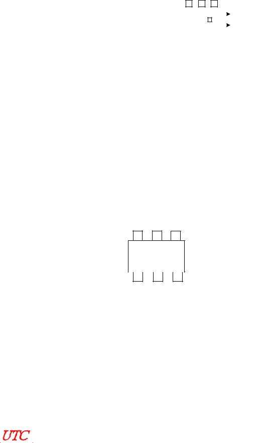
PIN CONFIGURATION
PIN DESCRIPTION
PIN NO. |
PIN NAME |
DESCRIPTION |
1 |
DO |
For discharge control: FET gate connection pin |
2 |
VM |
For current sense and charger detection input pin |
3 |
CO |
For charge control: FET gate connection pin |
4 |
DP |
Test pin for delay time measurement |
5 |
VDD |
Positive power input |
6 |
VSS |
Negative power input |
|
|
UNISONICTECHNOLOGIESCO.,LTD |
2 of 10 |
|
|
www.unisonic.com.tw |
QW-R502-A27.a |
|
|
|
|

UB261 |
Preliminary |
CMOS IC |
BLOCK DIAGRAM
VDD |
0V Battery Charge |
||
Inhibition Detector |
|||
|
|||
VM |
|
|
|
|
Oscillator |
|
|
Charger Detector |
|
Short circuit Detector |
|
|
Divider |
|
|
Overdischarge |
|
Over current 2 Detector |
|
Detector |
|
|
|
|
Control |
VM |
|
|
Logic |
||
Overcharge |
|
Over current 1 Detector |
|
Detector |
|
|
|
From Oscillator |
|
|
|
VSS |
|
|
|
DP |
DO |
CO |
|
|
|
UNISONICTECHNOLOGIESCO.,LTD |
3 of 10 |
|
|
www.unisonic.com.tw |
QW-R502-A27.a |
|
|
|
|

UB261 |
Preliminary |
CMOS IC |
ABSOLUTE MAXIMUM RATING (VSS=0V, TA=25°С unless otherwise specified)
PARAMETER |
SYMBOL |
RATINGS |
UNIT |
Input Voltage Between VDD and VSS (Note 2) |
VDD |
VSS-0.3 ~ VSS+12 |
V |
CO Output Pin Voltage |
VCO |
VDD-12 ~ VDD+0.3 |
V |
DO Output Pin Voltage |
VDO |
VSS-0.3 ~ VDD+0.3 |
V |
VM Input Pin Voltage |
VM |
VDD-14 ~ VDD+0.3 |
V |
Ambient Operating Temperature |
TOPR |
-40 ~ +85 |
°С |
Storage Temperature |
TSTG |
-55 ~ +125 |
°С |
Notes: 1. Absolute maximum ratings are those values beyond which the device could be permanently damaged. Absolute maximum ratings are stress ratings only and functional device operation is not implied.
2.Pulse (μsec) noise exceeding the above input voltage (VSS+12V) may cause damage to the IC.
ELECTRICAL CHARACTERISTICS (VSS=0V, TA=25°С unless otherwise specified)
PARAMETER |
SYMBOL |
TEST CONDITIONS |
MIN |
TYP |
MAX |
UNIT |
|
CURRENT CONSOMPTION |
|
|
|
|
|
|
|
Supply Current |
IOPE |
VDD=3.5V, VM=0V |
|
3.0 |
8.0 |
μA |
|
Power-Down Current |
IPDN |
VDD=VM=1.5V |
|
0.2 |
0.5 |
μA |
|
OPERATING VOLTAGE |
|
|
|
|
|
|
|
Operating Voltage Between VDD-pin and |
VDS1 |
|
1.5 |
|
8 |
V |
|
VSS-pin |
|
|
|||||
|
|
|
|
|
|
||
Operating Voltage Between VDD-pin and |
VDS2 |
|
1.5 |
|
10 |
V |
|
VM-pin |
|
|
|||||
|
|
|
|
|
|
||
DETECTION VOLTAGE |
|
|
|
|
|
|
|
Overcharge Detection Voltage |
VCU |
|
VCU-0.050 |
VCU |
VCU+0.050 |
V |
|
Overcharge Release Voltage |
VCL |
|
VCL-0.050 |
VCL |
VCL+0.050 |
V |
|
Overdischarge Detection Voltage |
VDL |
|
VDL-0.100 |
VDL |
VDL+0.100 |
V |
|
Overdischarge Release Voltage |
VDU |
|
VDU-0.100 |
VDU |
VDU+0.100 |
V |
|
Over Current 1 Detection Voltage |
VIOV1 |
VDD=3.5V |
VIOV1-0.03 |
VIOV1 |
VIOV1+0.03 |
V |
|
Over Current 2 Detection Voltage |
VIOV2 |
VDD=3.5V |
0.35 |
0.50 |
0.65 |
V |
|
Load Short Circuit Detection Voltage |
VSHORT |
|
0.5 |
1.2 |
1.7 |
V |
|
Charger Detection Voltage |
VCHA |
VDU≠VDL |
-1.6 |
-0.7 |
-0.2 |
V |
|
0V BATTERY CHARGE VOLTAGE |
|
|
|
|
|
|
|
0V Battery Charge Inhibition Battery |
V0INH |
|
|
0.9 |
1.8 |
V |
|
Voltage |
|
|
|||||
|
|
|
|
|
|
||
INTERNAL RESISTANCE |
|
|
|
|
|
|
|
Resistance between VM-pin and |
RVMD |
VDD=1.8V, VM=0V |
100 |
300 |
900 |
kΩ |
|
VDD-pin |
|||||||
|
|
|
|
|
|
||
Resistance between VM-pin and |
RVMS |
VDD=3.5V, VM=1.0V |
10 |
30 |
70 |
kΩ |
|
VSS-pin |
|||||||
|
|
|
|
|
|
||
OUTPUT RESISTANCE |
|
|
|
|
|
|
|
CO-pin Resistance “H” |
RCOH |
VCO=3.0V, VDD=3.5V, VM=0V |
|
5 |
10 |
kΩ |
|
CO-pin Resistance “L” |
RCOL |
VCO=0.5V, VDD=4.5V, VM=0V |
|
5 |
10 |
kΩ |
|
DO-pin Resistance “H” |
RDOH |
VDO=3.0V, VDD=3.5V, VM=0V |
|
5 |
10 |
kΩ |
|
DO-pin Resistance “L” |
RDOL |
VDO=0.5V, VDD=VM=1.8V |
|
5 |
10 |
kΩ |
|
DELAY TIME |
|
|
|
|
|
|
|
Overcharge Detection Delay Time |
tCU |
|
0.9 |
1.2 |
1.5 |
s |
|
Overdischarge Detection Delay Time |
tDL |
|
110 |
150 |
190 |
ms |
|
Over Current 1 Detection Delay Time |
tIOV1 |
VDD=3.5V |
6 |
9 |
12 |
ms |
|
Over Current 2 Detection Delay Time |
tIOV2 |
VDD=3.5V |
1 |
2.2 |
3.2 |
ms |
|
Short Circuit Detection Delay Time |
tSHORT |
|
120 |
300 |
380 |
µs |
|
|
UNISONICTECHNOLOGIESCO.,LTD |
4 of 10 |
|
|
www.unisonic.com.tw |
QW-R502-A27.a |
|
|
|
|
 Loading...