

Datasheet TS391AG-AF5, TS391AG-AL5, TS391BG-AF5, TS391BG-AL5, TS391CG-AF5 Datasheet (UTC) [ru]
...
UNISONIC TECHNOLOGIES CO., LTD
TS391/A/B/C
LINEAR INTEGRATED CIRCUIT
LOW POWER SINGLE VOLTAGE
COMPARATOR
DESCRIPTION
The UTC TS391/A/B/C consists of a low power voltage
comparator designed specifically to operate from a single supply
over a wide range of voltages. Operation from split power supplies is
also possible.
This comparator also has a unique characteristic in that the input
common-mode voltage range includes ground even though operated
from a single power supply voltage.
FEATURES
* Wide single supply voltage range or dual supplies +2V~+36V or
±1V~±18V
* Very low supply current (0.2mA) independent of supply voltage
(1mW /comparator at +5V)
* Low input bias current: 25nA typ.
* Low input offset current: ±5nA typ.
* Low input offset voltage: ±1mV typ
* Input common-mode voltage range includes ground.
* Low output saturation voltage: 250mV typ.(I
* Differential input voltage range equal to the supply voltage.
* TTL, DTL, ECL, CMOS Compatible outputs.
OUT
=4mA).
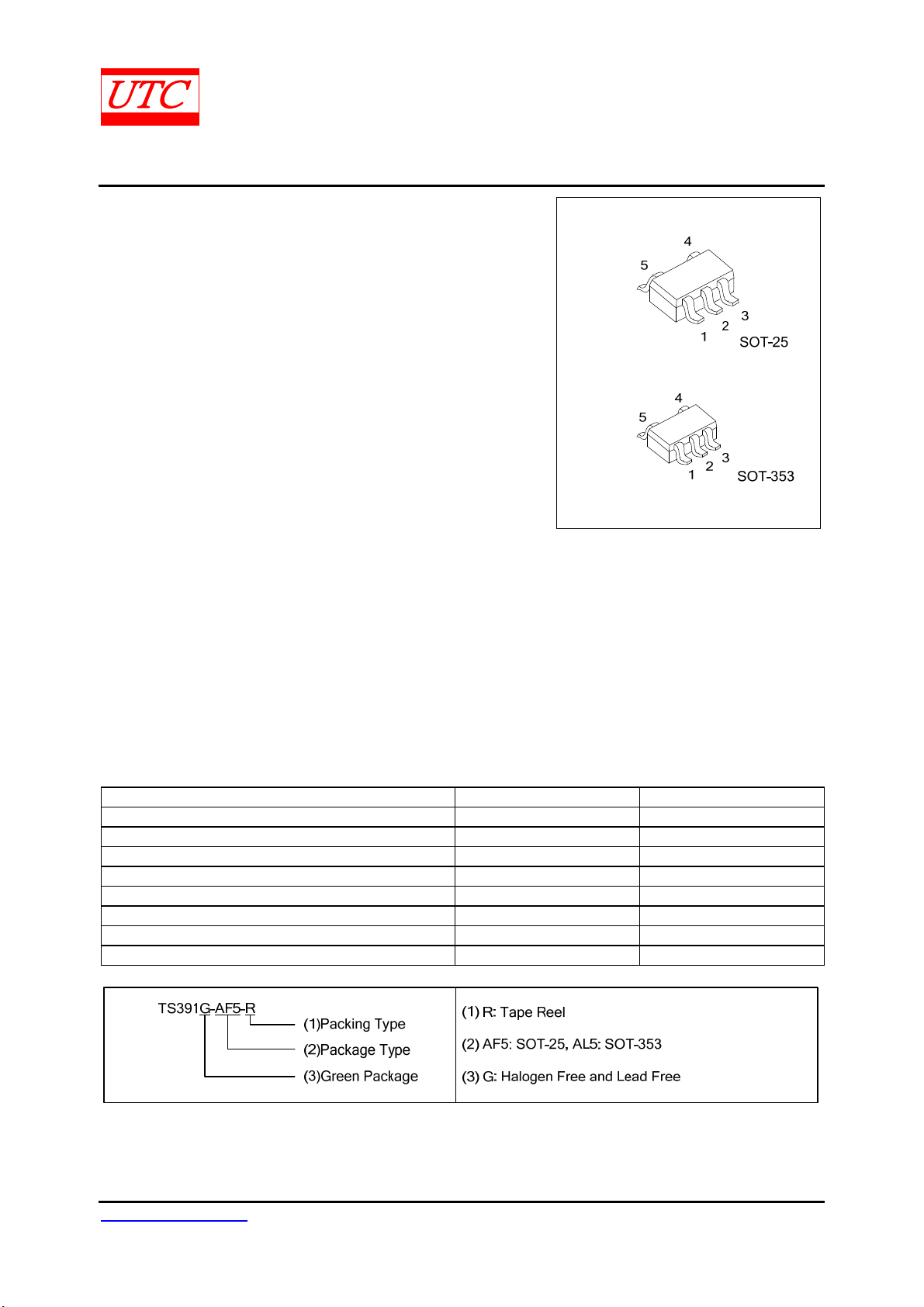
ORDERING INFORMATION
Ordering Number Package Packing
TS391G-AF5-R SOT-25 Tape Reel
TS391AG-AF5-R SOT-25 Tape Reel
TS391BG-AF5-R SOT-25 Tape Reel
TS391CG-AF5-R SOT-25 Tape Reel
TS391G-AL5-R SOT-353 Tape Reel
TS391AG-AL5-R SOT-353 Tape Reel
TS391BG-AL5-R SOT-353 Tape Reel
TS391CG-AL5-R SOT-353 Tape Reel
www.unisonic.com.tw 1 of 6
Copyright © 2015 Unisonic Technologies Co., Ltd QW-R104-003.I
TS391/A/B/C LINEAR INTEGRATED CIRCUIT
MARKING
TS391 TS391A
TS391B TS391C
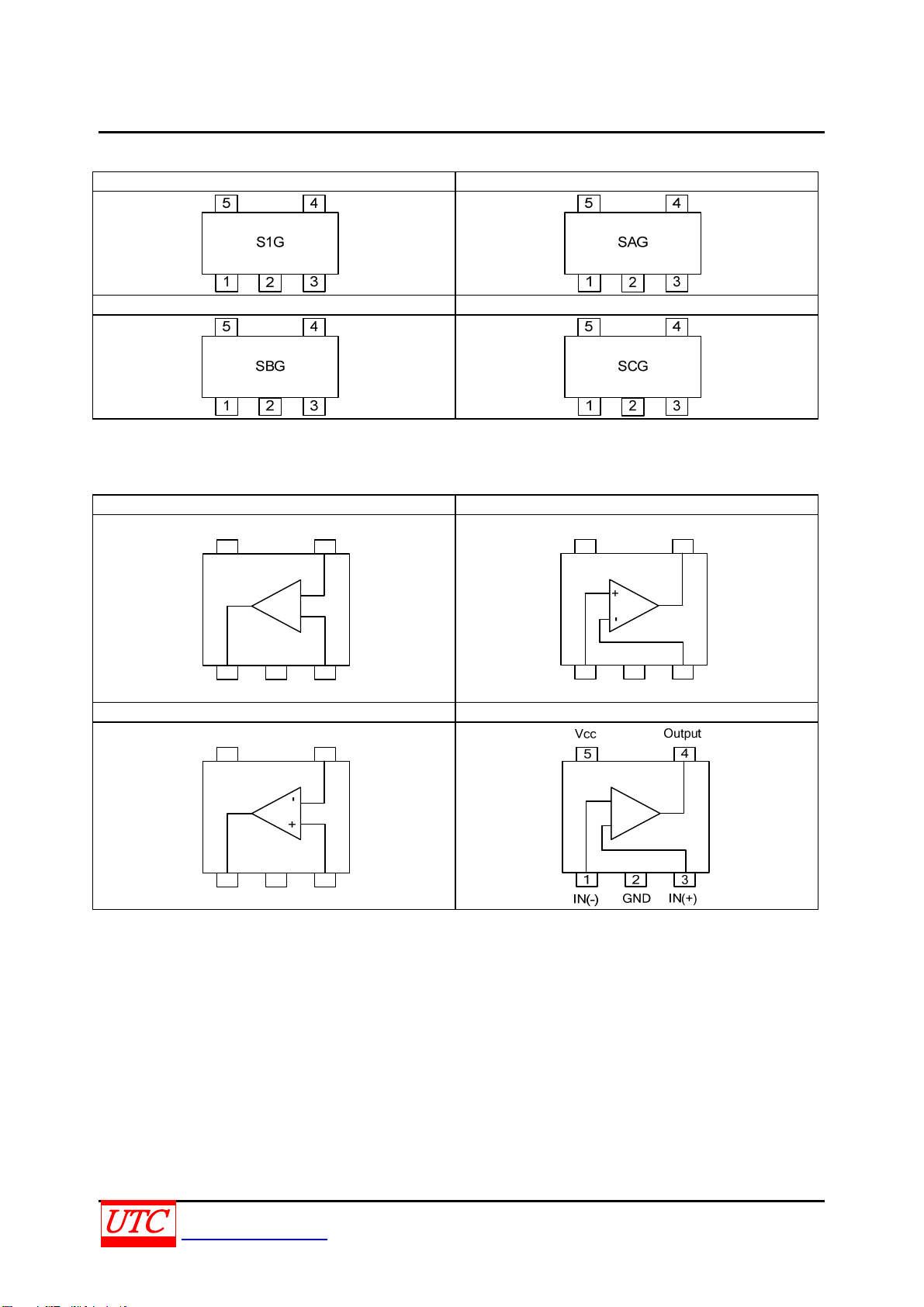
PIN CONNECTIONS
TS391 TS391A
Vcc
5
1
Output
Vcc
5
23
GND
TS391B TS391C
(top view)
IN(+)
4
+
-
IN(-)
IN(-)
4
Vcc Output
5
1
IN(+)
23
GND
4
IN(-)
+ -
1
Output
23
GND
IN(+)
UNISONIC TECHNOLOGIES CO., LTD 2 of 6
www.unisonic.com.tw QW-R104-003.I
TS391/A/B/C LINEAR INTEGRATED CIRCUIT
BLOCK DIAGRAM
V
+
CC
IN(+)
IN(-)
GND
3.5μA
100μA
3.5μA 100μA
GND
Output
GND
UNISONIC TECHNOLOGIES CO., LTD 3 of 6
www.unisonic.com.tw QW-R104-003.I

TS391/A/B/C LINEAR INTEGRATED CIRCUIT
ABSOLUTE MAXIMUM RATINGS
PARAMETER SYMBOL RATING UNIT
Supply Voltage VCC ±18 or 36 V
Differential Input Voltage V
Input Voltage VIN -0.3 ~ +36 V
Output Short-Circuit to Ground (Note 2) Infinite
Power Dissipation PD 500 mW
Junction Temperature TJ 150 °C
Operating Temperature T
Storage Temperature T
Notes: 1. Absolute maximum ratings are those values beyond which the device could be permanently damaged.
Absolute maximum ratings are stress ratings only and functional device operation is not implied.
2. Short-circuit from the output to V
can cause excessive heating and eventual destruction. The maximum
CC
output current is approximately 20mA, independent of the magnitude of V
THARMAL DATA (T
=150°C, TA=25°C)
J
PARAMETER SYMBOL RATING UNIT
Junction to Ambient JA 250 °C/W
ELECTRICAL CHARACTERISTICS
(VCC=5.0V, All voltage referenced to GND, TA=25°C, unless otherwise specified)
PARAMETER SYMBOL TEST CONDITIONS MIN TYP MAX UNIT
Input Offset Voltage (Note 1) V
Differential Input Voltage (Note 4) V
Large Signal Voltage Gain GV VCC=15V, RL=15k, V
Range (Note 3)
V
Low Level Output Voltage VOL
Input Bias Current (Note 2) I
I(BIAS)
Input Offset Current I
Supply Current ICC
Output sink current I
High Level Output Current IOH
Response Time tR RL=5.1k to VCC (Note 5) 1.3 s
Large Signal Response Time t
Notes: 1. At output switch point, Vo=1.4V, R
range (0V ~ V
1.5V).
CC
2. The direction of the input current is out of the IC due to the PNP input stage. This current is essentially
constant, independent of the state of the output, so no loading charge exists on the reference or input
lines.
3. The input common-mode voltage of either input signal voltage should not be allowed to go negative by
more than 0.3V.The upper end of the common-mode voltage range is V
can go to +30V without damage.
4. Positive excursions of input voltage may exceed the power supply level. As long as the other voltage
remains within the common-mode range the comparator will provide a proper output state.
The low input voltage state must not be less than -0.3V (or 0.3V below the negative power supply, if used).
5. The response time specified is for a 100mV input step with 5mV overdrive. For larger overdrive signals
300ns can be obtained.
TA=+25°C 1 5 mV
I(OFF)
T
MIN TA
VCC V
I(DIFF)
TA=+25° 0 VCC-1.5 V Input Common Mode Voltage
I(CM)
T
TA T
MIN
V
I(DIFF)
V
= V
CC
TA=+25° 25 250 nA
T
TA T
MIN
TA=+25° 5 50 nA
I(OFF)
T
TA T
MIN
VCC=5V, no load 0.2 0.5 mA
V
=30V, no load 0.5 1.25 mA
CC
V
SINK
REL
I(DIFF)
V
I(DIFF)
V
= V
CC
VIN=TTL,V
=0 with VCC from 5V ~ 30V and over the full input common-mode
S
±36 V
I(DIFF)
-40 ~ +125 °C
OPR
-65 ~ +150 °C
STG
.
CC
T
9 mV
MAX
=1~ 11V 50 200 V/mV
OUT
0 VCC -2 V
MAX
=1V,
=30V
OUT
MAX
MAX
=-1V, V
=1V,
=30V
OUT
=+1.4V,RL=5.1K~ V
REF
TA=+25°C 250 400 mV
T
MIN
TA T
700 mV
MAX
400 nA
150 nA
=1.5V 6 16 mA
OUT
TA=+25°C 0.1 nA
T
MIN
TA T
1 A
MAX
CC
300 ns
+ -1.5V,but either or both inputs
CC
UNISONIC TECHNOLOGIES CO., LTD 4 of 6
www.unisonic.com.tw QW-R104-003.I

TS391/A/B/C LINEAR INTEGRATED CIRCUIT
TYPICAL CHARACTERISTICS
Supply Current vs. Supply Voltage
0.5
)
0.4
A
m
(
t
n
0.3
e
r
r
u
C
0.2
y
l
p
p
u
S
0.1
0
0
10 20 30 40
Supply Voltage (V)
TA=-40°
TA=+25°
TA=+125°
R=
Input Voltage (mV) Output Voltage (V)
Input Current vs. Supply Voltage
80
)
60
A
n
(
t
n
e
r
r
40
u
C
t
u
p
n
I
20
TA=+25°
TA=+125°
TA=-40°
Response Time for vs. Input Overdrives
- Negative Transition
6
5
4
3
2
1
0
0
-50
-100
Input overdrive:5mV
20mV
100mV
00.511.52
Time (µS)
Response Time for vs. Input Overdrives
- Positive Transition
6
5
4
3
2
1
0
100
50
0
Input overdrive:100mV
20mV
TA=+25°
+5V
-
eI
+
TA=+25°
5mV
eI
+5V
+
5.1k
eo
5.1k
eo
0
10
20
30 40
Input Voltage (mV) Output Voltage (V)
Supply Voltage (V)
Output Saturation Voltage vs. Output Current
1
10
)
V
0
(
10
e
g
a
t
l
o
-1
V
10
n
o
i
t
a
r
u
t
-2
a
10
S
-3
10
-2
10
TA=+125°
10
Out of saturation
-1
TA=+25°
0
10
TA=-40°
1
10
10
2
Output Sink Current (mA)
0 0.5 1 1.5 2
Time (µS)
UNISONIC TECHNOLOGIES CO., LTD 5 of 6
www.unisonic.com.tw QW-R104-003.I

TS391/A/B/C LINEAR INTEGRATED CIRCUIT
UTC assumes no responsibility for equipment failures that result from using products at values that
exceed, even momentarily, rated values (such as maximum ratings, operating condition ranges, or
other parameters) listed in products specifications of any and all UTC products described or contained
herein. UTC products are not designed for use in life support appliances, devices or systems where
malfunction of these products can be reasonably expected to result in personal injury. Reproduction in
whole or in part is prohibited without the prior written consent of the copyright owner. The information
presented in this document does not form part of any quotation or contract, is believed to be accurate
and reliable and may be changed without notice.
UNISONIC TECHNOLOGIES CO., LTD 6 of 6
www.unisonic.com.tw QW-R104-003.I

 Loading...