

UNISONIC TECHNOLOGIES CO., LTD
TDA7377
LINEAR INTEGRATED CIRCUIT
2 x 30W DUAL/QUAD POWER
AMPLIFIER FOR CAR RADIO
DESCRIPTION
The UTC TDA7377 is a class AB car radio amplifier for car
radio, it can work either in dual bridge or quad single ended
configuration. The exclusive fully complementary structure of the
output stage and the internally fixed gain guarantees the highest
possible power performances with few external components. The
on-board clip detector simplifies gain compression operation. The
fault diagnostics makes it possible to detect mistakes during car
radio set assembly and wiring in the car.
FEATURES
* High Output Power@VCC=14.4V, f=1KHz,RL=4:
– 2 x 35W Max.
– 2 x 20W@THD= 10%
– 4 x 6 W @10%
– 4 x 10W / 2@10%
– 2 x 30W / EIAJ@ V
* CMOS Compatible Stand-by Function (Low I
* No Audible pop During st-by Operations
* Internally Fixed Gain (26dB BTL and 20dB single ended)
* No Bootstrap Capacitors and boucherot Cells
* Diagnostics Facility on pin10 when output Clipping, shorted to
Vcc or GND, thermal shutdown and soft short at turn on.
* Rail to rail output swing
* Absolute Stability Without Any External Compensation.
=13.7V,RL=4
CC
CC
)
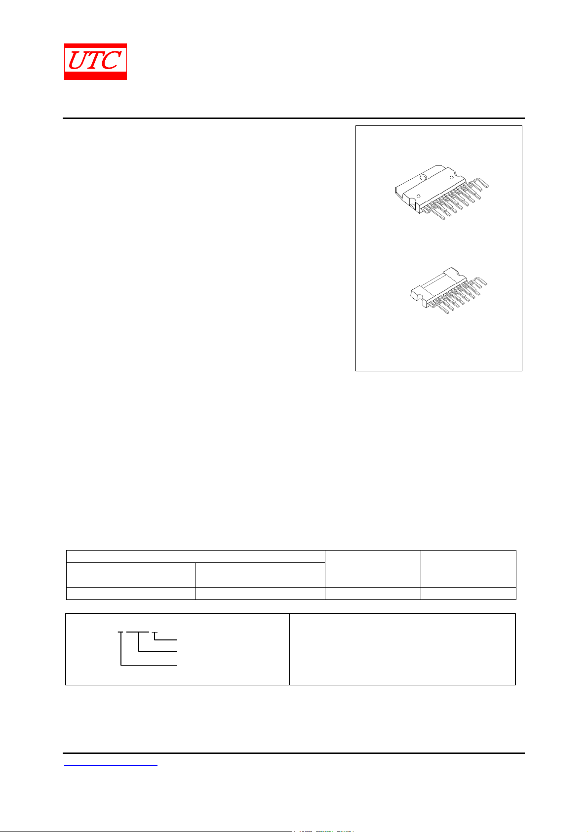
HZIP-15A
HZIP-15D
PROTECTIONS
* Load Dump Voltages surge
* Reversed Battery
* Output DC Short Circuit protecttion with
Low current when shorted to GND or V
* Output AC short circuit protection: across
the load
* Silent Turn On/Off
* thermal shutdown
* Load very Inductive speakers
* Fortuitous Open GND
* ESD
CC
.
ORDERING INFORMATION
Ordering Number
Lead Free Halogen Free
TDA7266L-J15-A-T TDA7266G-J15-A-T HZIP-15A Tube
TDA7377L-J15-D-T TDA7377G-J15-D-T HZIP-15D Tube
TDA7377L-J15-A-T
(1) Packing Type
(2) Package Type
(3) Lead Free
www.unisonic.com.tw 1 of 10
Copyright © 2012 Unisonic Technologies Co., Ltd
QW-R107-064.B
(1) T: Tube
(2) J15-A:HZIP-15A, J15-D: HZIP-15D
(3) G: Halogen Free, L: Lead Free
Package Packing
TDA7377 LINEAR INTEGRATED CIRCUIT
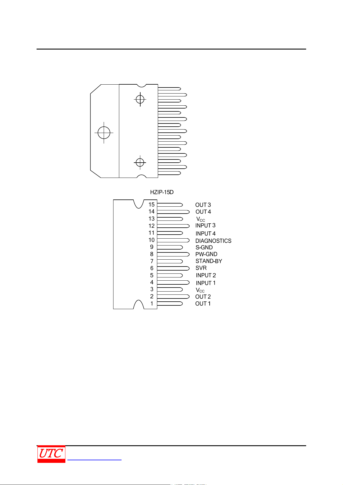
PIN CONNECTION
HZIP-15A
15
14
13
12
11
10
OUT 3
OUT 4
V
CC
INPUT 3
INPUT 4
DIAGNOSTICS
9
8
7
6
5
4
3
2
1
S-GND
PW-GND
STAND-BY
SVR
INPUT 2
INPUT 1
V
CC
OUT 2
OUT 1
UNISONIC TECHNOLOGIES CO., LTD 2 of 10
www.unisonic.com.tw QW-R107-064.B

TDA7377 LINEAR INTEGRATED CIRCUIT
BLOCK DIAGRAM
VCC VCC
A1
+
-
1
OUT 1
IN 1
4
13 3
ST - BY
IN 2
IN 3
IN 4
7
5
12
11
A2 1NV
+
-
A3
+
-
A4 1NV
+
-
986
PW - GNDSVR S - GND
2
15
14
10
OUT 2
OUT 3
OUT 4
DIAGNOSTICS
UNISONIC TECHNOLOGIES CO., LTD 3 of 10
www.unisonic.com.tw QW-R107-064.B
TDA7377 LINEAR INTEGRATED CIRCUIT
)
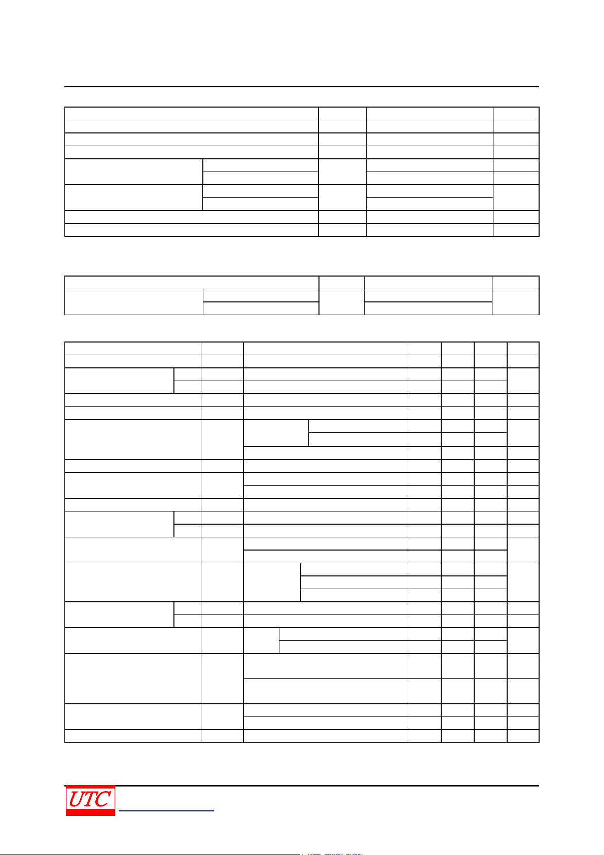
ABSOLUTE MAXIMUM RATINGS
PARAMETER SYMBOL RATINGS UNIT
Operating Supply Voltage VOP 18 V
DC Supply Voltage VS 28 V
Peak Supply Voltage (for t = 50ms) V
Output Peak Current
Power Dissipation (TC= 70°C)
not Repetitive t = 100µs
Repetitive f >10Hz 3.5 A
HZIP-15A
HZIP-15D 30
S(PEAK
I
O(PEAK)
PD
Junction Temperature TJ +150 °C
Storage Temperature T
-40~+150 °C
STG
Note: Absolute maximum ratings are those values beyond which the device could be permanently damaged.
Absolute maximum ratings are stress ratings only and functional device operation is not implied.
THERMAL DATA
PARAMETER SYMBOL RATINGS UNIT
Junction to Case
HZIP-15A
HZIP-15D 1.8
JC
ELECTRICAL CHARACTERISTICS
(VS = 14.4V; RL = 4; f = 1 KHz; Ta =25°C, unless otherwise specified)
PARAMETER SYMBOL TEST CONDITIONS MIN TYP MAX UNIT
Supply Voltage Range VS 8 18 V
ST-BY Threshold Voltage
IN V
OUT V
Voltage Saturation on pin 10 V
Output Offset Voltage V
Input Noise Voltage eN
Total Quiescent Drain Current IQ RL = 150 mA
ST-BY Pin Current(pin 7) I
ST-BY Current Consumption I
Clipping Detector Output
Average Current
OFF I
ON I
Input Impedance RIN
Output Power P
Output Power (Note 3)
Max P
EIAJ P
Distortion THD RL = 4
Cross Talk CT
Voltage Gain GV
Voltage Gain Match GV 0.5 dB
1.5
I(ST-BY)
3.5
O(ST-BY)
Sink Current at Pin 10 = 1mA 0.7 V
SAT
150 mV
O(OFF)
Rg = 0; S.E.
”A” weighted,
Non Inverting Channels 2
Inverting Channels 5
Bridge, Rg = 0; 22Hz ~ 22KHz 3.5 µV
Max Driving Current Under Fault 5 mA
ST-BY
Play Mode Vpin7 = 5V 50 µA
V
ST-BY
d = 1% (Note 2) 90 µA
CD(OFF)
d = 5% (Note 2) 160 µA
CD(ON)
= 0 ~ 1.5V 100 µA
ST-BY
Single Ended 20 30
Bridge 10 15
THD = 10%;
OUT
R
= 4
L
VS = 14.4V, Bridge 31 35 W
O(MAX)
VS = 13.7V, Bridge 27 30 W
O(EIAJ)
Bridge 18 20
Single Ended 5.5 6
Single Ended, RL = 2 10
Single Ended, P
Bridge, P
OUT
=0.1~4W 0.02
OUT
= 0.1 ~ 10W 0.03 0.3
f = 1KHz Single Ended
f = 10KHz Single Ended
f = 1KHz Bridge
f = 10KHz Bridge
Single Ended 19 20 21 dB
Bridge 25 26 27 dB
50 V
4.5 A
33 W
1.4
°C/W
V
µV
K
W
%
dB
dB
dB
dB
55
70
60
60
UNISONIC TECHNOLOGIES CO., LTD 4 of 10
www.unisonic.com.tw QW-R107-064.B

TDA7377 LINEAR INTEGRATED CIRCUIT
ELECTRICAL CHARACTERISTICS(Cont.)
Supply Voltage Rejection SVR Rg = 0; f = 300Hz 50 dB
Stand-by Attenuation A
Note: 1. See built-in S/C protection description
2. Pin 10 Pulled-up to 5V with 10K; RL = 4
3. Saturated square wave output.
PO = 1W 80 90 dB
ST-BY
UNISONIC TECHNOLOGIES CO., LTD 5 of 10
www.unisonic.com.tw QW-R107-064.B

TDA7377 LINEAR INTEGRATED CIRCUIT
TYPICAL TEST AND APPLICATION CIRCUIT
UNISONIC TECHNOLOGIES CO., LTD 6 of 10
www.unisonic.com.tw QW-R107-064.B

TDA7377 LINEAR INTEGRATED CIRCUIT
ST-BY
IN L
IN L
IN BRIDGE
10K
0.22μF
0.22μF
0.47μF
47μF
10μF
4
5
12
11
6
89
DIAGNOSTICS
Figure 3. Stereo/Bridge
3137
100nF
10
15
14
1
2
2200μF
2200μF
S
V
1000μF
OUT L
OUT R
OUT
BRIDGE
UNISONIC TECHNOLOGIES CO., LTD 7 of 10
www.unisonic.com.tw QW-R107-064.B

TDA7377 LINEAR INTEGRATED CIRCUIT
TYPICAL APPLICATION INFORMATION
Diagnostics Facility note:
UTC TDA7377 built in a diagnostic circuitry, when following events appearing: clipping in the output signal,
thermal shutdown, and output fault including short to GND, short to V
When the event is detected, The information is available across an open collector output (pin 10) through a current
sinking (see Fig 4).The current sinking at pin 10 is triggered when a certain distortion level is reached at any of the
outputs. This function allows gain compression possibility whenever the amplifier is overdriven. The current sinking
at pin 10 also can be triggered When the IC’s operating temperature raise to about 10°C before the shutdown
threshold.
Normally the clip detector signaling produces a low level at pin 10 that is shorter than that present under faulty
conditions; This can be used to discriminate each event (clipping detection, output fault, thermal proximity).
and soft short at turn on.
S
10
UTC TDA7377
Figure 4. Pin10 Diagnostic Circuitry
R
V
10
PIN
V
REF
-
UNISONIC TECHNOLOGIES CO., LTD 8 of 10
www.unisonic.com.tw QW-R107-064.B

TDA7377 LINEAR INTEGRATED CIRCUIT
TYPICAL CHARACTERISTICS
UNISONIC TECHNOLOGIES CO., LTD 9 of 10
www.unisonic.com.tw QW-R107-064.B

TDA7377 LINEAR INTEGRATED CIRCUIT
UTC assumes no responsibility for equipment failures that result from using products at values that
exceed, even m omentarily, rated values (such as maximum ratings, operating condition ranges, or
other parameters) listed in products specifications of any and all UTC products described or contained
herein. UTC products are not designed for use in life support appliances, devices or systems where
malfunction of these products can be reasonably expected to result in personal injury. Reproduction in
whole or in part is prohibited without the prior written consent of the copyright owner. The inform ation
presented in this document does not form part of any quotation or contract, is believed to be accurate
and reliable and may be changed without notice.
UNISONIC TECHNOLOGIES CO., LTD 10 of 10
www.unisonic.com.tw QW-R107-064.B

 Loading...