

UNISONIC TECHNOLOGIES CO., LTD
TDA7375
LINEAR INTEGRATED CIRCUIT
2 x 35W DUAL/QUAD POWER
AMPLIFIER FOR CAR RADIO
DESCRIPTION
The UTC TDA7375 is a class AB car radio amplifier for car radio,
it can work either in dual bridge or quad single ended configuration.
The exclusive fully complementary structure of the output stage
and the internally fixed gain guarantees the highest possible power
performances with few external components. The on-board clip
detector simplifies gain compression operation. The fault
diagnostics makes it possible to detect mistakes during car radio
set assembly and wiring in the car.
FEATURES
* High output power capability:
– 2 x 40W Max. / 4
– 2 x 25W / 4@14.4V, 1KHz, 10%
– 2 x 35W / 4 EIAJ
– 4 x 7 W / 4@14.4V, 1KHz, 10%
– 4 x 12W / 2@14.4V, 1KHz, 10%
* Minimum external components:
– No bootstrap capacitors
– No Boucherot cells
– Internally fixed gain (26dB BTL)
* Stand-by function (CMOS compatible)
* No audible pop during st-by operations
* Diagnostics facility for:
– Clipping
– Out to GND short
– Out to V
– Soft short at turn-on
– Thermal shutdown proximity
short
S
Lead-free: TDA7375L
Halogen-free:TDA7375G
PROTECTIONS
* Output AC/DC short circuit
– to GND
– to V
S
– across the load
* Soft short at turn-on
* Overrating chip temperature with soft
thermal limiter
* Load dump voltages urge
* Very inductive loads
* Fortuitous open GND
* Reversed battery
* ESD
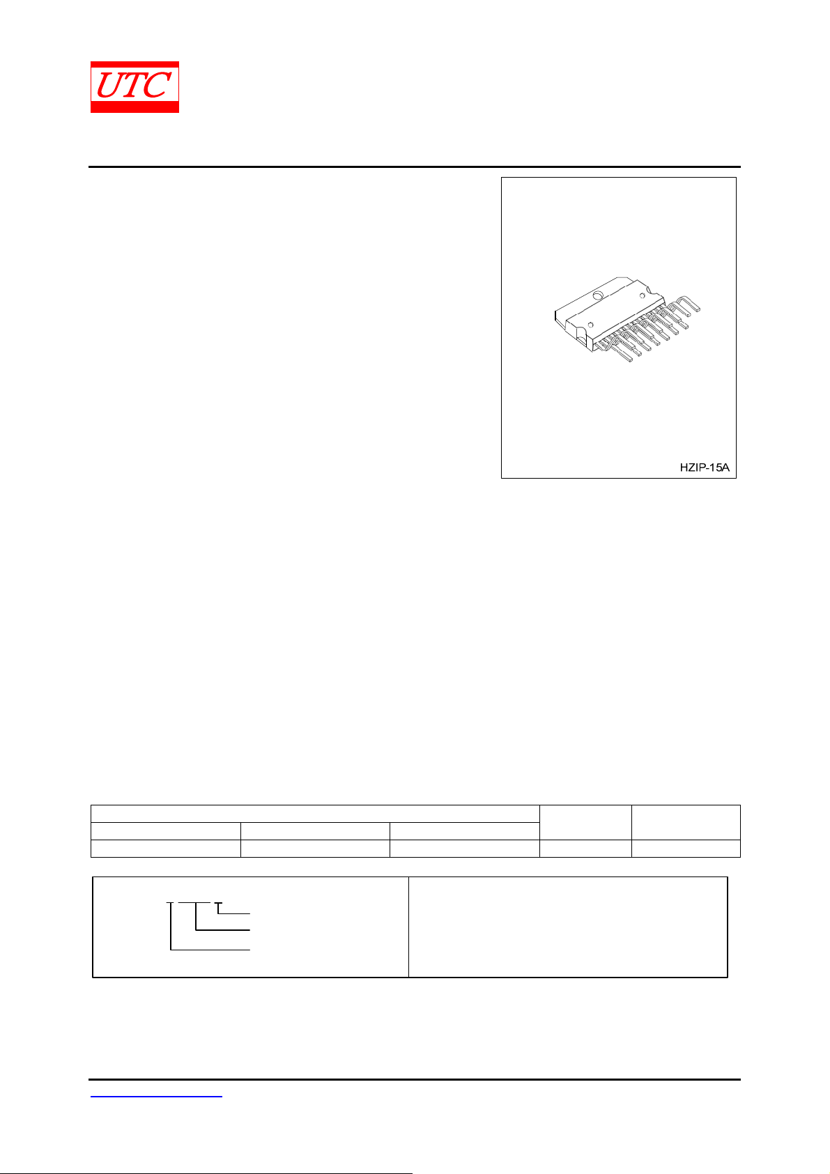
ORDERING INFORMATION
Ordering Number
Normal Lead Free Plating Halogen Free
TDA7375-J15-A-T TDA7375L-J15-A-T TDA7375G-J15-A-T HZIP-15A Tube
TDA7375L-J15-A-T
(1) Packing Type
(2) Package Type
(3) Lead Plating
www.unisonic.com.tw 1 of 9
Copyright © 2009 Unisonic Technologies Co., Ltd QW-R107-046.C
(1) T: Tube
(2) J15-A: HZIP-15A
(3) G: Halogen Free, L: Lead Free, Blank: Pb/Sn
Package Packing

TDA7375 LINEAR INTEGRATED CIRCUIT
PIN CONNECTION (Top view)
15
14
13
12
11
10
9
8
7
6
5
4
3
2
1
BLOCK DIAGRAM
OUT 3
OUT 4
CC
V
INPUT 3
INPUT 4
DIAGNOSTICS
S - GND
PW - GND
STAND - BY
SVR
INPUT 2
INPUT 1
CC
V
OUT 2
OUT 1
VCC VCC
A1
+
-
A2 1NV
+
-
A3
+
-
A4 1NV
+
-
1
2
15
14
10
OUT 1
OUT 2
OUT 3
OUT 4
DIAGNOSTICS
IN 1
ST - BY
IN 2
IN 3
IN 4
4
7
5
12
11
13 3
986
PW - GNDSVR S - GND
UNISONIC TECHNOLOGIES CO., LTD 2 of 9
www.unisonic.com.tw QW-R107-046.C
TDA7375 LINEAR INTEGRATED CIRCUIT
ABSOLUTE MAXIMUM RATINGS
PARAMETER SYMBOL RATINGS UNIT
Operating Supply Voltage VOP 18 V
DC Supply Voltage VS 28 V
Peak Supply Voltage (for t = 50ms) V
Output Peak Current
not repetitive t = 100µs 4.5 A
repetitive f >10Hz
S(PEAK)
I
O(PEAK)
Power Dissipation (TC= 85°C) PD 36 W
Junction Temperature TJ +150 °C
Storage Temperature T
-40~+150 °C
STG, TJ
Note: Absolute maximum ratings are those values beyond which the device could be permanently damaged.
Absolute maximum ratings are stress ratings only and functional device operation is not implied.
THERMAL DATA
PARAMETER SYMBOL RATINGS UNIT
Junction to Case JC 1.8 °C/W
ELECTRICAL CHARACTERISTICS
(VS = 14.4V; RL = 4; f = 1 KHz; Ta =25°C, unless otherwise specified)
PARAMETER SYMBOL TEST CONDITIONS MIN TYP MAX UNIT
Supply Voltage Range VS 8 18 V
ST-BY Threshold Voltage
IN V
OUT V
Voltage Saturation on pin 10 V
Output Offset Voltage V
Input Noise Voltage eN
Total Quiescent Drain Current IQ RL = 200 mA
ST-BY Pin Current(pin 7) I
ST-BY Current Consumption I
OFF I
Average Current
ON I
Input Impedance RIN
Output Power P
Output Power (Note 3)
Max. P
EIAJ P
Distortion THD RL = 4
Cross Talk CT
Voltage Gain GV
Voltage Gain Match GV 0.5 dB
Supply Voltage Rejection SVR Rg = 0; f = 300Hz 50 dB
Stand-by Attenuation A
Notes: 1. See built-in S/C protection description
2. Pin 10 Pulled-up to 5V with 10K; RL = 4
3. Saturated square wave output.
1.5
I(ST-BY)
3.5
O(ST-BY)
Sink Current at Pin 10 = 1mA 0.7 V
SAT
150 mV
O(OFF)
Rg = 0; S.E.
”A” weighted,
Non Inverting Channels 2
Inverting Channels 5
Bridge, Rg = 0; 22Hz ~ 22KHz 3.5 µV
Max Driving Current Under Fault 5 mA
ST-BY
Play Mode Vpin7 = 5V 50 µA
V
ST-BY
d = 1% (Note 2) 90 µA Clipping Detector Output
CD(OFF)
d = 5% (Note 2) 160 µA
CD(ON)
= 0 ~ 1.5V 100 µA
ST-BY
Single Ended 20 30
Bridge 10 15
THD = 10%;
OUT
R
= 4
L
VS = 14.4V, Bridge 36 40 W
O(MAX)
VS = 13.7V, Bridge 32 35 W
O(EIAJ)
Bridge 23 25
Single Ended 6.5 7
Single Ended, R
Single Ended, P
Bridge, P
= 0.1 ~ 10W 0.03 0.3
OUT
= 2 12
L
=0.1~4W 0.02
OUT
f = 1KHz Single Ended
f = 10KHz Single Ended
f = 1KHz Bridge
f = 10KHz Bridge
Single Ended 19 20 21 dB
Bridge 25 26 27 dB
PO = 1W 80 90 dB
ST-BY
50 V
3.5 A
V
µV
K
W
%
70
60
55
60
dB
dB
dB
dB
UNISONIC TECHNOLOGIES CO., LTD 3 of 9
www.unisonic.com.tw QW-R107-046.C

TDA7375 LINEAR INTEGRATED CIRCUIT
TYPICAL TEST AND APPLICATION CIRCUIT
Note:
C9, C10, C11, C12 could be
reduced if the 2Ω operation is not
required.
ST-BY
IN FL
IN FR
IN RL
IN RR
10K R1
C1 0.22μF
C2 0.22μF
C4 0.22μF
C3 0.22μF
C8 47μF
Figure 1: Quad Stereo
C7
10μF
4
5
12
11
6
89
C6
100nF
3137
1
2
15
14
10
DIAGNOSTICS
C10 2200μF
C9 2200μF
C11 2200μF
C12 2200μF
V
S
C5
1000μF
OUT FL
OUT FR
OUT RL
OUT RR
Figure 2: Double Bridge
ST-BY
IN L
IN L
IN BRIDGE
10K
0.22μ F
0.22μ F
0.47μ F
47μ F
10μ F
4
5
12
11
6
89
3137
1
2
15
14
10
DIAGNOSTICS
2200μ F
2200μ F
V
1000μ F100nF
OUT L
OUT R
OUT
BRIDGE
S
Figure 3: Stereo/Bridge
UNISONIC TECHNOLOGIES CO., LTD 4 of 9
www.unisonic.com.tw QW-R107-046.C

TDA7375 LINEAR INTEGRATED CIRCUIT
TYPICAL APPLICATION INFORMATION
1. High Application Flexibility
It is possible that accomplish several kinds of applications ranging from 4 speakers stereo (F/R) to 2 speakers
bridge solutions with 4 independent channels
In order to avoid phase inconveniences causing sound alterations especially during the reproduction of low
frequencies. When working in single ended conditions the polarity of the speakers driven by the inverting
amplifier must be reversed respect to those driven by non inverting channels.
2. Easy Single Ended to Bridge Transition
The change from single ended to bridge configurations is made simply by means of a short circuit across the
inputs, further external component is unnecessary.
3. Gain Internally Fixed to 20dB in Single Ended, 26dB in Bridge
The function advantages not only to save component, PCB space but also optimize output noise, supply
voltage rejection and distortion
4. Silent Turn On/Off and Muting/Stand-by Function
The stand-by can be easily activated by means of a CMOS level applied to pin 7 through a RC filter. Under
stand-by condition the device is turned off completely (Vs=1mA typ.; A
Every ON/OFF operation is virtually pop free. Furthermore, at turn-on the device stays in muting condition for a
time determined by the value assigned to the SVR capacitor. While in muting the device outputs becomes
insensitive to any kinds of signal that may be present at the input terminals.
ST-BY= 80dB min.).
5 .STAND-BY DRIVING (pin 7)
The definition of stand-by driving networks is most important that pin 7 cannot be directly driven by a voltage
source whose current capability is higher than 5mA. In practical cases a series resistance has always to be
inserted to limit the current at pin 7 and to smooth down the stand-by ON/OFF transitions - in combination with
a capacitor - for output pop prevention. In any case, a capacitor of at least 100nF from pin 7 to S-GND, with no
resistance in between, is necessary to ensure correct turn-on.
6. BUILT–IN SHORTCIRCUIT PROTECTION
Reliable and safe operation, in presence of all kinds of short circuit involving the outputs is assured by
BUILT-IN protectors. Additionally to the AC/DC short circuit to GND, to V
SHORT condition is signaled out during the TURN-ON PHASE so assuring correct operation for the device
itself and for the loudspeaker.
This particular kind of protection acts in a way to avoid that the device is turned on (by ST-BY) when a resistive
path (less than 16 ohms) is present between the output and GND. As the involved circuitry is normally disabled
when a current higher than 5mA is flowing into the ST-BY pin, it is important, in order not to disable it, to have
the external current source driving the STBY pin limited to 5mA.
This extra function becomes particularly attractive when, in the single ended configuration, one capacitor is
shared between two outputs (see Fig. 4).
Supposing that the output capacitor COUT for any reason is shorted, the loudspeaker will not be damaged being
this soft short circuit condition revealed.
Figure 4.
COUT
, across the speaker, a SOFT
S
UNISONIC TECHNOLOGIES CO., LTD 5 of 9
www.unisonic.com.tw QW-R107-046.C

TDA7375 LINEAR INTEGRATED CIRCUIT
z Diagnostics Facility
The IC is equipped with a diagnostic circuitry able to detect clipping in the output signal, thermal shutdown,
and output fault including short to GND, short to V
The information is available across an open collector output (pin 10) through a current sinking when the
event is detected.
soft short at turn on.
S and
Vo
AUDIO
OUTPUT
SIGNAL
CL IPPING
ICL IP
0
DET.
OUTPUT CURR.
time
Figure 5: Clipping Detection Waveforms
A current sinking at pin 10 is triggered when a certain distortion level is reached at any of the outputs. This
function allows gain compression possibility whenever the amplifier is overdriven.
z Thermal Shutdown
In this case the output 10 will signal the proximity of the junction temperature to the shutdown threshold.
Typically current sinking at pin 10 will start ~10°C before the shutdown threshold is reached.
7. HANDLING OF THE DIAGNOSTICS SIGNAL
Since various kinds of information is available at the same pin (clipping detection, output fault, thermal
proximity), this signal must be handled properly in order to discriminate each event. This could be done by
taking into account the different timing of the diagnostic output during each case.
ST-BY PIN
VOLTAGE
2V
UTC TDA7375
10
R
REF
V
OUTPUT
WAVEFORM
Upi n 10
OUT TO GND SHORT
Vpin 10
CHECK AT TURN-ON
(TEST PHASE)
CORRECT TURN-ON
OUT TO Vs SHORT
SOFT SHORT
FAULT DETECTION
Figure 6: Output Fault Waveforms (see Fig. 7) Figure 7: Fault Waveforms
SHORT TO GND
OR TO Vs
t
t
t
UNISONIC TECHNOLOGIES CO., LTD 6 of 9
www.unisonic.com.tw QW-R107-046.C

TDA7375 LINEAR INTEGRATED CIRCUIT
ST-BY PIN
VOLTAGE
t
Vs
OUTPUT
WAVEFORM
t
Vpin 10
WAVEFORM
CLIPPING
SHORT TO GND
OR TO Vs
THERMAL
PROXIMITY
t
Figure 8: Waveforms
Normally the clip detector signalling produces a low level at pin 10 that is shorter than that present under faulty
conditions; based on this assumption an interface circuitry to differentiate the information is represented in the
schematic of Fig. 9.
Figure 9.
8. PCB-LAYOUT GROUNDING
The device has 2 distinct ground leads, P-GND (POWER GROUND) and S-GND (SIGNAL GROUND) which
are practically disconnected from each other at chip level. Proper operation requires that P-GND and S-GND
leads be connected together on the PCB-layout by means of reasonably low-resistance tracks.
As to the PCB-ground configuration, a starlike arrangement whose center is represented by the supply-filtering
electrolytic capacitor ground is highly advisable. In such context, at least 2 separate paths have to be provided,
one for P-GND and one for S-GND. The correct ground assignments are as follows:
- STANDBY CAPACITOR(pin 7, or any other standby driving networks): on S-GND
- SVR CAPACITOR (pin 6): on S-GND and to be placed as close as possible to the device.
- INPUT SIGNAL GROUND (from active/passive signal processor stages): on S-GND.
- SUPPLY FILTERING CAPACITORS (pins 3,13): on P-GND. The (-) terminal of the electrolytic capacitor
has to be directly tied to the battery (-) line and this should represent the starting point for all the ground
paths.
UNISONIC TECHNOLOGIES CO., LTD 7 of 9
www.unisonic.com.tw QW-R107-046.C

TDA7375 LINEAR INTEGRATED CIRCUIT
TYPICAL CHARACTERISTICS
UNISONIC TECHNOLOGIES CO., LTD 8 of 9
www.unisonic.com.tw QW-R107-046.C

TDA7375 LINEAR INTEGRATED CIRCUIT
UTC assumes no responsibility for equipment failures that result from using products at values that
exceed, even m omentarily, rated values (such as maximum ratings, operating condition ranges, or
other parameters) listed in products specifications of any and all UTC products described or contained
herein. UTC products are not designed for use in life support appliances, devices or systems where
malfunction of these products can be reasonably expected to result in personal injury. Reproduction in
whole or in part is prohibited without the prior written consent of the copyright owner. The inform ation
presented in this document does not form part of any quotation or contract, is believed to be accurate
and reliable and may be changed without notice.
UNISONIC TECHNOLOGIES CO., LTD 9 of 9
www.unisonic.com.tw QW-R107-046.C

 Loading...