

UTC TDA7266G-J15-A, TDA7266G-J15-B, TDA7266G-J15-D, TDA7266L-J15-A, TDA7266L-J15-B Schematic [ru]
...
UNISONIC TECHNOLOGIES CO., LTD
TDA7266 LINEAR INTEGRATED CIRCUIT
7+7W DUAL BRIDGE
AMPLIFIER
DESCRIPTION
The UTC TDA7266 is a 7+7W dual bridge amplifier specially
designed for TV and Portable Radio applications.
FEATURES
* Wide Supply Voltage Range (3 ~ 18V)
* Minimum External Components
* No SWR Capacitor
* No Bootstrap
* No Boucherot Cells
* Internally Fixed Gain
* Stand-BY & Mute Functions
* Short Circuit Protection
* Thermal Overload Protection
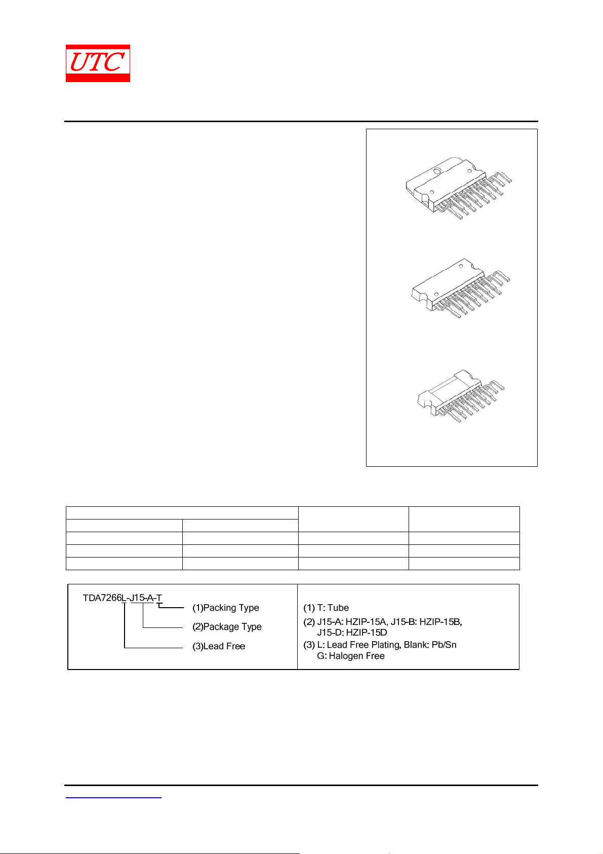
HZIP-15A
HZIP-15B
ORDERING INFORMATION
Ordering Number
Lead Free Halogen Free
TDA7266L-J15-A-T TDA7266G-J15-A-T HZIP-15A Tube
TDA7266L-J15-B-T TDA7266G-J15-B-T HZIP-15B Tube
TDA7266L-J15-D-T TDA7266G-J15-D-T HZIP-15D Tube
Package Packing
HZIP-15D
www.unisonic.com.tw 1 of 8
Copyright © 2010 Unisonic Technologies Co., Ltd QW-R107-037,C
TDA7266 LINEAR INTEGRATED CIRCUIT
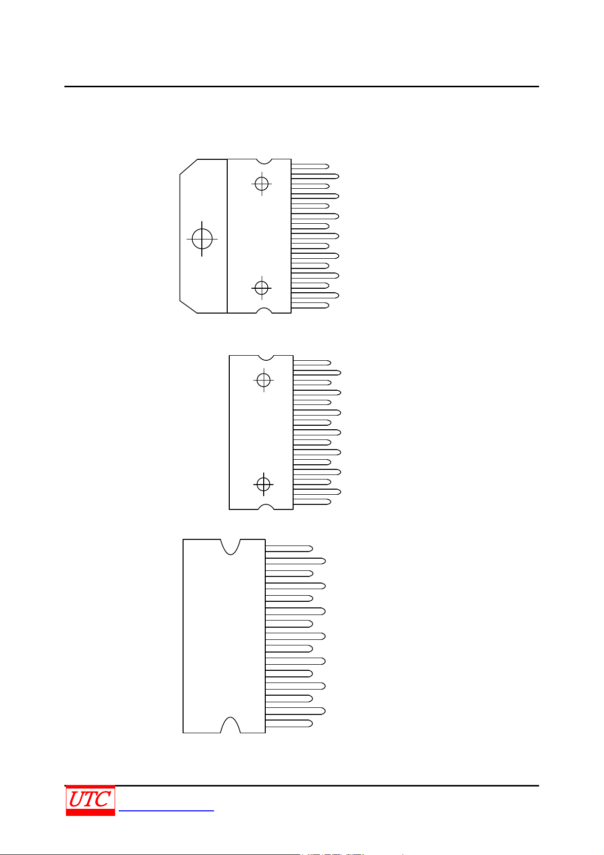
PIN CONFIGURATION
HZIP-15A
15
14
13
12
11
10
9
8
7
6
5
4
3
2
1
OUT2+
OUT2Vcc
IN2
N.C.
N.C.
S-GND
PW-GND
STAND-BY(ST-BY)
MUTE
N.C.
IN1
Vcc
OUT1OUT1+
HZIP-15B
15
14
13
12
11
10
9
8
7
6
5
4
3
2
1
OUT2+
OUT2-
Vcc
IN2
N.C.
N.C.
S-GND
PW-GND
STAND-BY(ST-BY)
MUTE
N.C.
IN1
Vcc
OUT1-
OUT1+
HZIP-15D
15
14
13
12
11
10
9
8
7
6
5
4
3
2
1
OUT 2+
OUT 2V
CC
IN 2
N.C.
N.C.
S-GND
PW-GND
STAND-BY(ST-BY)
MUTE
N.C.
IN 1
V
CC
OUT 1OUT 1+
UNISONIC TECHNOLOGIES CO., LTD 2 of 8
www.unisonic.com.tw QW-R107-037,C
TDA7266 LINEAR INTEGRATED CIRCUIT
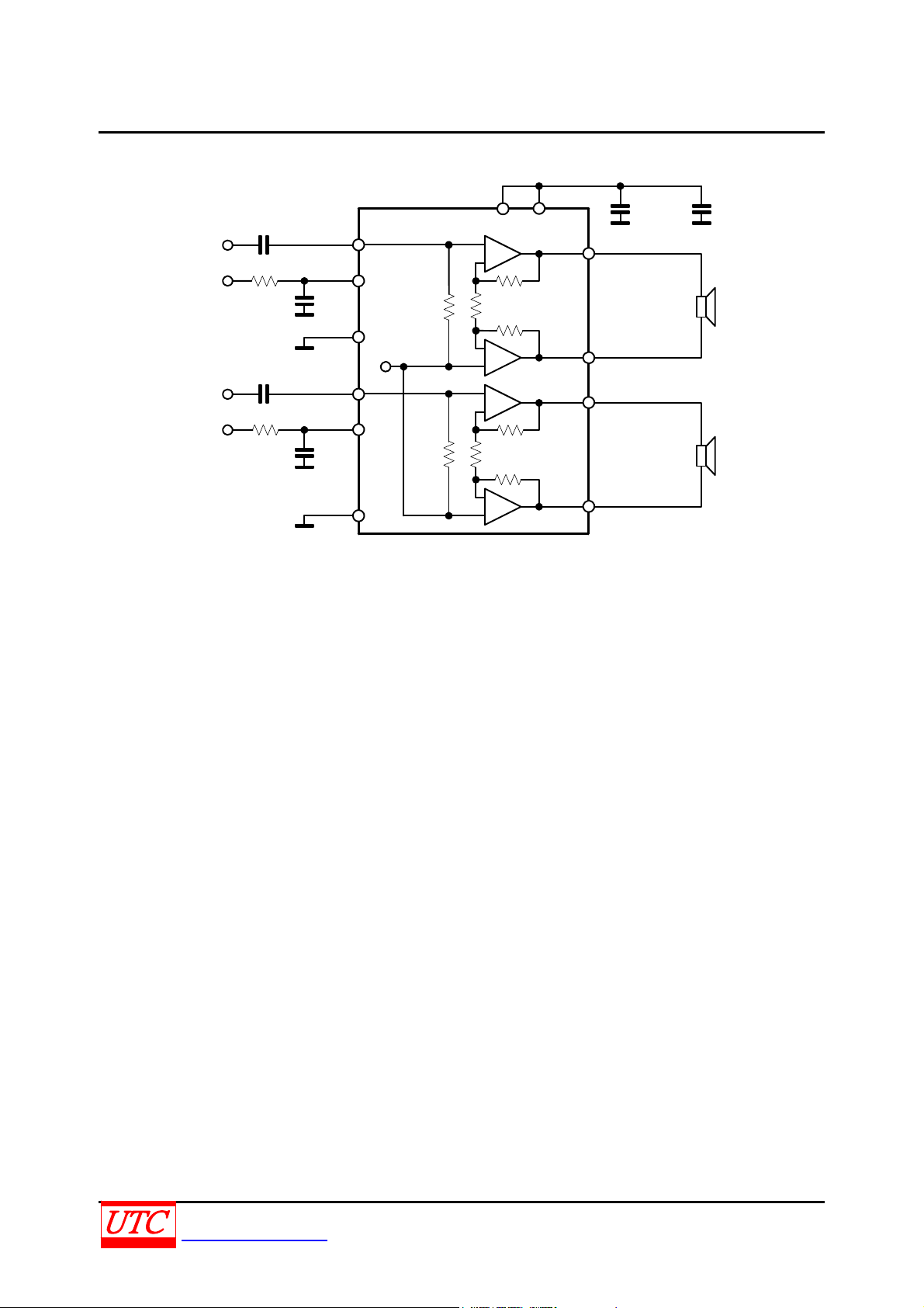
BLOCK DIAGRAM
Vcc
IN1
ST-BY
IN2
MUTE
0.22µF
0.22µF
PW-GND
S-GND
4
9
V
12
8
7
REF
6
470µF
100nF
133
1
15
14
2
OUT1+
OUT1-
OUT2+
OUT2-
+
-
-
+
+
-
-
+
UNISONIC TECHNOLOGIES CO., LTD 3 of 8
www.unisonic.com.tw QW-R107-037,C

TDA7266 LINEAR INTEGRATED CIRCUIT
ABSOLUTE MAXIMUM RATINGS
PARAMETER SYMBOL RATINGS UNIT
Supply Voltage VCC 20 V
Output Peak Current (internally limited) I
Power Dissipation (TC =70°C)
HZIP-15A / HZIP-15B 33
HZIP-15D
Junction Temperature TJ +125
Operating Junction Temperature TJ 0 ~ +70
Storage Temperature T
Note: Absolute maximum ratings are those values beyond which the device could be permanently damaged.
Absolute maximum ratings are stress ratings only and functional device operation is not implied.
THERMAL DATA
PARAMETER SYMBOL RATINGS UNIT
Junction to Case
HZIP-15A / HZIP-15B 1.4
HZIP-15D
2 A
OUT
P
D
20
W
°C
°C
-40 ~ +150
STG
θJC
2.5
°C
°C /W
ELECTRICAL CHARACTERISTICS(V
=11V, R
CC
=8Ω, f=1kHz, Ta=25°C, unless otherwise specified)
L
PARAMETER SYMBOL TEST CONDITIONS MIN TYP MAX UNIT
Supply Range VCC 3 11 18 V
Output Offset Voltage V
) 120 mV
O(OFF
Total Output Noise Voltage eN A curve, f=20Hz ~ 20kHz 150 μV
Total Quiescent Current IQ 48 65 mA
Input Resistance RIN 25 30 kΩ
Output Power P
Total Harmonic Distortion THD
THD=10% 6.3 7 W
OUT
P
=1W 0.05 0.2 %
OUT
P
=0.1~2W, f=100Hz~15kHz 1 %
OUT
Crosstalk CT 46 60 dB
Closed Loop Voltage Gain Gv 25 26 27 dB
Voltage Gain Matching △Gv 0.5 dB
Supply Voltage Rejection SVR f=100Hz, VR=0.5V 40 56 dB
Thermal Threshold Tt 150
°C
MUTE FUNCTION
Mute Threshold VM
Mute Attenuation A
for VCC>6.4V, V
THD
for V
<6.4V, V
CC
60 80 dB
MUTE
= -30dB 2.3 2.9 4.1 V
OUT
= -30dB
OUT
VCC/2-1.0
VCC/2-0.75
VCC/2-0.5
V
STAND BY FUNCTION
STAND-BY Threshold VT
STAND-BY Current V6=GND I
0.8 1.3 1.8 V
ST-BY
100 μA
ST-BY
UNISONIC TECHNOLOGIES CO., LTD 4 of 8
www.unisonic.com.tw QW-R107-037,C

TDA7266 LINEAR INTEGRATED CIRCUIT
APPLICATION SUGGESTION
For Microprocessor Application
In order to avoid annoying ”Pop-Noise” during Turn-On/Off transients, it is necessary to guarantee the right ST-BY
and MUTE signals sequence. It is quite simple to obtain this function using a microprocessor (Fig 1 and Fig 2).
At first ST-BY signal (from mP) goes high and the voltage across the ST-BY terminal (Pin 7) starts to increase
exponentially. The external RC network is intended to turn-on slowly the biasing circuits of the amplifier, this to
avoid ”POP” and ”CLICK” on the outputs.
When this voltage reaches the ST-BY threshold level, the amplifier is switched-on and the external capacitors in
series to the input terminals (C3, C5) start to charge.
It’s necessary to maintain the mute signal low until the capacitors are fully charged, this to avoid that the device
goes in play mode causing a loud “Pop Noise” on the speakers.
A delay of 100 ~ 200ms between ST-BY and MUTE signals is suitable for a proper operation.
Vcc
µP
ST-BY
IN2
MUTE
IN1
C1
0.22µF
R1
10k
C3
0.22µF
R2
10k
C2
10µF
S-GND
C4
1µF
12
4
7
9
133
1
2
TDA7266
15
6
OUT1+
OUT1-
OUT2+
C5
470µF
C6
100nF
OUT2-
PW-GND
8
14
Fig. 1 Microprocessor Application
UNISONIC TECHNOLOGIES CO., LTD 5 of 8
www.unisonic.com.tw QW-R107-037,C

TDA7266 LINEAR INTEGRATED CIRCUIT
APPLICATION SUGGESTION(Cont.)
+Vcc(V)
+18
IN (mV)
V
V
ST-BY
Pin 7
1.8
1.3
0.8
V
MUTE
Pin 6
Q (mA)
I
OUT (V)
V
4.1
2.9
2.3
OFF
ST-BY
MUTE
PLAY MUTE ST-BY OFF
Fig 2 Microprocessor Driving Signals
UNISONIC TECHNOLOGIES CO., LTD 6 of 8
www.unisonic.com.tw QW-R107-037,C

TDA7266 LINEAR INTEGRATED CIRCUIT
APPLICATION SUGGESTION(Cont.)
For Low Cost Application
In low cost applications where the mP is not present, the suggested circuit is shown in Fig 3.
The ST-BY and mute terminals are tied together and they are connected to the supply line via an external voltage
divider.
The device is switched-on/off from the supply line and the external capacitor C4 is intended to delay the ST-BY
and MUTE threshold exceeding, avoiding “Popping” problems.
Vcc
Vcc
R1
47k
R2
47k
C4
10µF
IN1
IN2
C3
0.22µF
C5
0.22µF
ST-BY
S-GND
12
4
7
9
TDA7266
133
1
2
15
OUT1+
OUT1-
OUT2+
C1
470µF
C2
100nF
MUTE
PW-GND
6
OUT2-
14
8
Fig 3 Stand Alone Low Cost Application
UNISONIC TECHNOLOGIES CO., LTD 7 of 8
www.unisonic.com.tw QW-R107-037,C

TDA7266 LINEAR INTEGRATED CIRCUIT
TYPICAL CHARACTERISTICS
5.0000
4.0000
3.0000
2.0000
1.0000
-1.000
Level (dBr)
-2.000
-3.000
-4.000
-5.000
0.0
10
Vcc=11V
R
I=8O
P
OUT=1W
Gain vs Frequency
10
0
1k
Frequency (Hz)
10k
100k
UTC assumes no responsibility for equipment failures that result from using products at values that
exceed, even momentarily, rated values (such as maximum ratings, operating condition ranges, or
other parameters) listed in products specifications of any and all UTC products described or contained
herein. UTC products are not designed for use in life support appliances, devices or systems where
malfunction of these products can be reasonably expected to result in personal injury. Reproduction in
whole or in part is prohibited without the prior written consent of the copyright owner. The information
presented in this document does not form part of any quotation or contract, is believed to be accurate
and reliable and may be changed without notice.
Quiescent Current vs Supply Voltage
70
65
60
50
IQ (mA)
45
40
35
30
3
4
7558
5
6910
Vsupply (V)
11
121314 15 16 17 18
UNISONIC TECHNOLOGIES CO., LTD 8 of 8
www.unisonic.com.tw QW-R107-037,C

 Loading...