

UNISONIC TECHNOLOGIES CO., LTD
W
LR1148 CMOS IC
600mA LO
REGULATOR
DESCRIPTION
The UTC LR1148 belonged to low-noise, low-dropout, linear
regulators operate from 2.3V to 6V input and are guaranteed to
deliver 600mA. Wide range of preset output voltage options are
available. Built-in low on-resistance transistor provides low dropout
voltage and large output current. The UTC LR1148 is designed and
optimized for battery-powered systems to work with low noise.
The UTC LR1148 consumes less than 0.01μA in shutdown
mode. Other features include ultra low dropout voltage, current
limiting protection, thermal shutdown protection and high ripple
rejection ratio.
FEATURES
* 600mA Guaranteed Output Current
* 0.01μA Shutdown Current
* Ultra Low Dropout Voltage
* Low Temperature Coefficient
* Current Limiting Protection
* Thermal Shutdown Protection
* Excellent Line/Load Transient
DROPOUT LINEAR
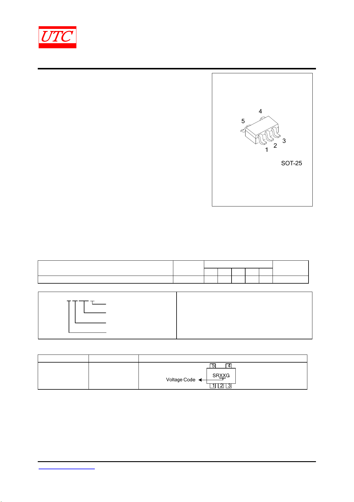
ORDERING INFORMATION
Ordering Number Package
LR1148G-xx-AF5-R SOT-25 I G S A O Tape Reel
Note: Pin Assignment: I:VIN O:V
LR1148G-xx-AF5-R
(1)Packing Type
(2)Package Type
(3)Output Voltage Code
(4)Green Package
G:GND S:EN A: ADJ
OUT
(1) R: Tape Reel
(2) AF5: SOT-25
(3) xx: refer to Marking Information
(4) G: Halogen Free and Lead Free
Pin Assignment
1234 5
MARKING INFORMATION
PACKAGE VOLTAGE CODE MARKING
SOT-25 AD: ADJ
Packing
www.unisonic.com.tw 1 of 4
Copyright © 2014 Unisonic Technologies Co., Ltd QW-R502 -A74.b
LR1148 CMOS IC
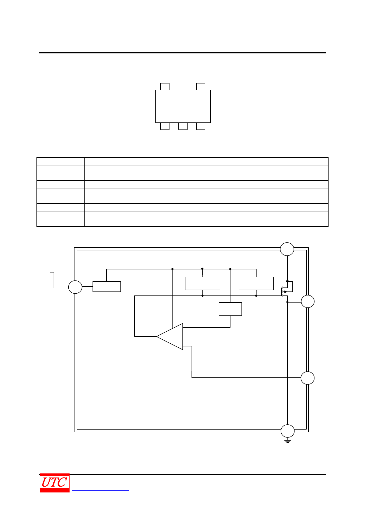
PIN CONFIGURATION
V
OUT
ADJ
45
2
1
GND
V
IN
3
EN
PIN DESCRIPTION
PIN NAME DESCRIPTION
VIN
GND Ground
EN
V
Output Voltage
OUT
ADJ
BLOCK DIAGRAM
Power Input Voltage. Supply voltage can range from 2.3V to 6V. Bypass with a 1µF capacitor to
GND.
Active-Low Shutdown Input. A logic low at EN reduces supply current to 0.01µA. Connect EN to
V
for normal operation.
IN
Voltage-adjust Input. Connect an external resistive voltage-divider from V
output voltage between 0.8V and 5V.
to ADJ to set the
OUT
V
IN
ON
Thermal
Sensor
EN
SHDN
Current Limit
OFF
V
OUT
V
REF
-
AMP
+
ADJ
GND
UNISONIC TECHNOLOGIES CO., LTD 2 of 4
www.unisonic.com.tw QW-R502-A74.b

LR1148 CMOS IC
)
)
T
T
A
A
ABSOLUTE MAXIMUM RATING (T
=25°С)
A
PARAMETER SYMBOL RATINGS UNIT
Supply Voltage V
6.5 V
IN
Power Dissipation PD 360 mW
Junction Temperature TJ +125 °С
Ambient Operating Temperature T
Storage Temperature T
-40 ~ +85 °С
OPR
-65 ~ +150 °С
STG
Note: Absolute maximum ratings are those values beyond which the device could be permanently damaged.
Absolute maximum ratings are stress ratings only and functional device operation is not implied.
THERMAL DATA
PARAMETER SYMBOL RATINGS UNIT
Junction to Ambient θ
JA
Junction to Case θJC 81 C/W
ELECTRICAL CHARACTERISTICS
(CIN = 1µF, C
=1µF, TA= 25°C, unless otherwise specified)(Note 1)
OUT
PARAMETER SYMBOL TEST CONDITIONS MIN TYP MAX UNIT
Input Voltage(Note 2) VIN 2.3 6 V
T
=25°С , I
Output Voltage Accuracy
(Preset Mode)
Maximum Output Current I
Short-Circuit Current Limit I
Ground Pin Current I
V
OUT
LIMIT
GND
OUT
Dropout Voltage (Note3) VD I
∆V
Line Regulation (Note4)
Load Regulation(Note4,5) ∆V
OUT
V×∆V
OUT
OUTIN
A
TA=0~85°С, I
600 mA
V
OUT
= 0mA 70 µA
I
OUT
I
= 1mA to 600mA 80 µA
OUT
=600mA
OUT
VIN=V
V
IN=VOUT+VD
I
=10mA~600mA
OUT
=0V 1 A
OUT+VD
= 1mA ~0.6A
OUT
= 1mA~0.6A
OUT
V
OUT(NOM
1.8V<V
<=1.8V 500 1200
OUT(NOM
~6V 0.08 0.55 %/V
,
Output Voltage Noise eN f=10Hz to100kHz, CBP=0.1nF 24
Shutdown Supply Current I
Shutdown Threshold
hermal Shutdown Temperature T
hermal Shutdown Hysteresis DT
DJ Voltage V
EN=GND 0.01 5 µA
OFF
V
IH
VIL 0.4 V
SHDN
SHDN
REF
170 °С
20 °С
Measured on ADJ, I
=10mA 0.774 0.8 0.826 V
OUT
djustable Output Voltage 0.8 5 V
Note: 1. Specifications are production tested at TA=25°C. Pecifications over the -40°C to 85°C operating temperature
range are assured by design, characterization and correlation with Statistical Quality Controls(SQC).
2. The minimum operating value for V
is equal to either [V
IN
OUT(NOM)+VD
3. Dropout voltage is defined as the voltage from the input to output when output is 2% below the nominal
value.
4. Output voltage line regulation is defined as the change in output voltage from the nominal value resulting
from a change in the input line voltage. Output voltage load regulation is defined as the change in output
voltage from the nominal value as the load current increases from no load to full load.
5. Regulation is measured at constant junction temperature by using a 20ms current pulse. Devices are tested
for load regulation in the load range from 10mA to 600mA.
260 C/W
-2 2 %
-3 3 %
200 450
0.25 1.0 %
2 V
] or 2.3V,whichever is greater
mV
µV
RM
S
UNISONIC TECHNOLOGIES CO., LTD 3 of 4
www.unisonic.com.tw QW-R502-A74.b

LR1148 CMOS IC
TYPICAL APPLICATION CIRCUIT
UNISONIC TECHNOLOGIES CO., LTD 4 of 4
www.unisonic.com.tw QW-R502-A74.b

 Loading...