

UTC LR1120G-18-AF5-A-R, LR1120G-18-AL5-A-R, LR1120G-25-AF5-A-R, LR1120G-25-AL5-A-R, LR1120G-28-AF5-A-R Schematic [ru]
...
UNISONIC TECHNOLOGIES CO., LTD
LR1120
Preliminary CMOS IC
500mA, LOW DROPOUT, LOW
NOISE ULTRA-FAST WITH
SOFT START CMOS LDO
REGULATOR
DESCRIPTION
UTC LR1120, a 500mA LDO regulator, has very high PSRR and
super low dropout voltage especially suitable for wireless and
portable applications.
In the field of hand-held wireless devices, board space and
battery life are the main concerns of designers and end-users.
Because of the low quiescent current and low ESR ceramic
capacitors, UTC LR1120 can satisfy those concerns.
Furthermore, low current consumption in shutdown mode
(0.7μA), fast turn-on time (<70μs), high output accuracy, current
limiting protection, and high ripple rejection ratio are advantages of
UTC LR1120.
FEATURES
* Operating Voltage Ranges : 2.2V to 5.5V
* Dropout : 250mV at 500mA
* When IC Shutdown: 5mA Discharge Current of V
* Extreme Low Noise for DSC Application
* Extreme Fast Response in Line/Load Transient
* Internal Current Limiting Protection
* Internal Thermal Shutdown Protection
* High PSRR
* Recommended 1μF Output Capacitor only for Stability
* With TTL Logic Controlled Shutdown Input
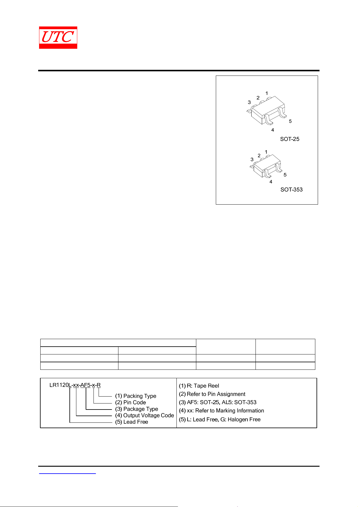
ORDERING INFORMATION
Ordering Number
Lead Free Halogen Free
LR1120L-xx-AF5-x-R LR1120G-xx-AF5-x-R SOT-25 Tape Reel
LR1120L-xx-AL5-x-R LR1120G-xx-AL5-x-R SOT-353 Tape Reel
Note: xx: Output Voltage, refer to Marking Information.
OUT
Package Packing
www.unisonic.com.tw 1 of 5
Copyright © 2013 Unisonic Technologies Co., Ltd QW-R502-331.j
LR1120 Preliminary CMOS IC
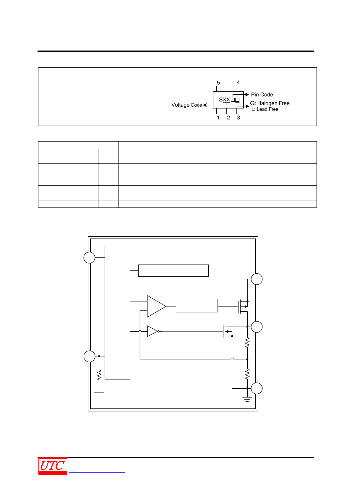
MARKING INFORMATION
PACKAGE VOLTAGE CODE MARKING
18 :1.8V
25 :2.5V
SOT-25
SOT-353
PIN DESCRIPTION
28 :2.8V
30: 3.0V
31 :3.1V
33 :3.3V
40 :4.0V
PIN CODE
A B C D
1 1 1 2 VIN Supply voltage input.
2 2 2 1 GND Ground.
3 3 3 - EN
4 - - - SS Soft start pin.
5 4 5 3 V
- 5 4 4, 5 NC No Connection
PIN
NAME
Input logic pin, active high for enabling the chip. When this pin goes to
a logic low, the chip will be shutdown.
Regulator output voltage pin.
OUT
BLOCK DIAGRAM
SS
Current Limit
V
REF
POR
OTP
+
MOS Driver
DESCRIPTION
V
IN
V
OUT
EN
R
GND
UNISONIC TECHNOLOGIES CO., LTD 2 of 5
www.unisonic.com.tw QW-R502-331.j

LR1120 Preliminary CMOS IC
ABSOLUTE MAXIMUM RATING (T
= 25°C, unless otherwise specified.)
A
PARAMETER SYMBOL RATINGS UNIT
Supply Input Voltage VIN 6 V
EN Input Voltage VEN 6 V
Power Dissipation (TA = 25°C)
SOT-25 0.38 W
SOT-353
PD
0.25 W
Junction Temperature TJ 150 °C
Storage Temperature T
STG
-65~ +150
°C
Note: Absolute maximum ratings are those values beyond which the device could be permanently damaged.
Absolute maximum ratings are stress ratings only and functional device operation is not implied.
THERMAL DATA
PARAMETER SYMBOL RATINGS UNIT
Junction to Ambient
SOT-25 260 °C/W
SOT-353
θJA
400 °C/W
OPERATING CONDITIONS
PARAMETER SYMBOL RATINGS UNIT
Supply Input Voltage VIN 2.2 ~ 5.5 V
Junction Temperature TJ -40 ~ +125 °C
Ambient Temperature TA -40 ~ +85 °C
Note: The device is not guaranteed to function outside its operating conditions.
ELECTRICAL CHARACTERISTICS
= V
(V
IN
+ 0.5V, VEN = VIN, CIN = C
OUT
= 1μF (Ceramic), TA= 25°C, unless otherwise specified.)
OUT
PARAMETER SYMBOL TEST CONDITIONS MIN TYP MAX UNIT
Input Voltage VIN 2.2 5.5 V
Output Voltage Accuracy ΔV
Line Regulation
Load Regulation (Note 1)
Quiescent Current (Note 2) IQ VEN = 5V, I
Standby Current I
Current Limit I
Dropout Voltage (Note 3) VD
Soft Start Time V
EN Threshold
Logic-Low VIL 0 0.6 V
Logic-High V
I
OUT
VΔ
OUT
OUTIN
V×VΔ
VΔ
OUT
OUT
V
VEN = 0V 0.7 1.5 μA
STN-BY
LIMIT
1.6 5.5 V
IH
= 10mA -2 0 +2 %
OUT
V
= (V
IN
1mA<I
1mA<I
R
LOAD
R
LOAD
I
OUT
I
OUT
OUT
+0.5V) ~ 5.5V, I
OUT
<400mA, 2.2V≤VIN<2.7V 0.6 %
OUT
<500mA, 2.7 V≤VIN≤5.5V 1 %
OUT
= 0mA 25 50 μA
OUT
= 1mA 0.01 0.2 %/V
OUT
= 0Ω, 2.2V≤VIN<2.7V 0.4 0.7 1.05 A
= 0Ω, 2.7V≤VIN≤5.5V 0.5 0.8 1.05 A
= 400mA, 2.2V≤VIN ≤2.7V 160 320
= 500mA, 2.7V≤VIN ≤5.5V 250 400
= 2.5V, CSS = 1nF, C
= 1μF 0.7 1 ms
OUT
mV
Enable Pin Current IEN 0.1 1 5 μA
Over Temperature Shutdown OTS 170 °C
Over Temperature Hysteresis OTH 30 °C
Power Supply Rejection Rate PSRR I
Output Noise Voltage e
N
= 10mA, f = 10kHz 55 dB
OUT
V
OUT
=1.5V,C
OUT
=1μF,I
=0mA, CSS = 1nF 40 μV
OUT
RMS
Note: 1. Regulation is measured at constant junction temperature by using a 2ms current pulse. Devices are tested
for load regulation in the load range from 1mA to 500mA.
2. Quiescent, or ground current, is the difference between input and output currents. It is defined by IQ = IIN I
under no load condition (I
OUT
= 0mA). The total current drawn from the supply is the sum of the load
OUT
current plus the ground pin current.
3. The dropout voltage is defined as V
-V
, which is measured when V
IN
OUT
OUT
is V
OUT(NORMAL)
×98%.
UNISONIC TECHNOLOGIES CO., LTD 3 of 5
www.unisonic.com.tw QW-R502-331.j

LR1120 Preliminary CMOS IC
TYPICAL APPLICATION CIRCUIT
V
V
IN
CIN=1μF
V
IN
V
OUT
OUT
C
=1μF
OUT
Chip Enable
EN
GND
SS
CSS=1nF
UNISONIC TECHNOLOGIES CO., LTD 4 of 5
www.unisonic.com.tw QW-R502-331.j

LR1120 Preliminary CMOS IC
UTC assumes no responsibility for equipment failures that result from using products at values that
exceed, even momentarily, rated values (such as maximum ratings, operating condition ranges, or
other parameters) listed in products specifications of any and all UTC products described or contained
herein. UTC products are not designed for use in life support appliances, devices or systems where
malfunction of these products can be reasonably expected to result in personal injury. Reproduction in
whole or in part is prohibited without the prior written consent of the copyright owner. The information
presented in this document does not form part of any quotation or contract, is believed to be accurate
and reliable and may be changed without notice.
UNISONIC TECHNOLOGIES CO., LTD 5 of 5
www.unisonic.com.tw QW-R502-331.j

 Loading...