

UNISONIC TECHNOLOGIES CO., LTD
L5200
LOW NOISE, REGULATED
CHARGE PUMP DC/DC
CONVERTERS
DESCRIPTION
The UTC L5200-xx series are low noise, constant frequency
charge pump DC/DC converters and designed to increase efficiency
in white LED application. The operating voltage range is 2.7V ~ V
input with up to 100mA of output current. Low external parts counts
(one flying capacitor and two small bypass capacitors at V
) make the UTC L5200-xx series ideally suited for small,
V
OUT
battery-powered applications.
A charge-pump architecture maintains constant switching
frequency to zero load and reduces both output and input ripple. The
UTC L5200-xx series have thermal shutdown capability to escape
the device damaged from a continuous short-circuit. With built-in
soft-start circuitry to prevents excessive current flow at V
start-up. High switching frequency enables the use of small ceramic
capacitors. A low-current shutdown feature disconnects the load from
V
and reduces quiescent current to <1μA.
IN
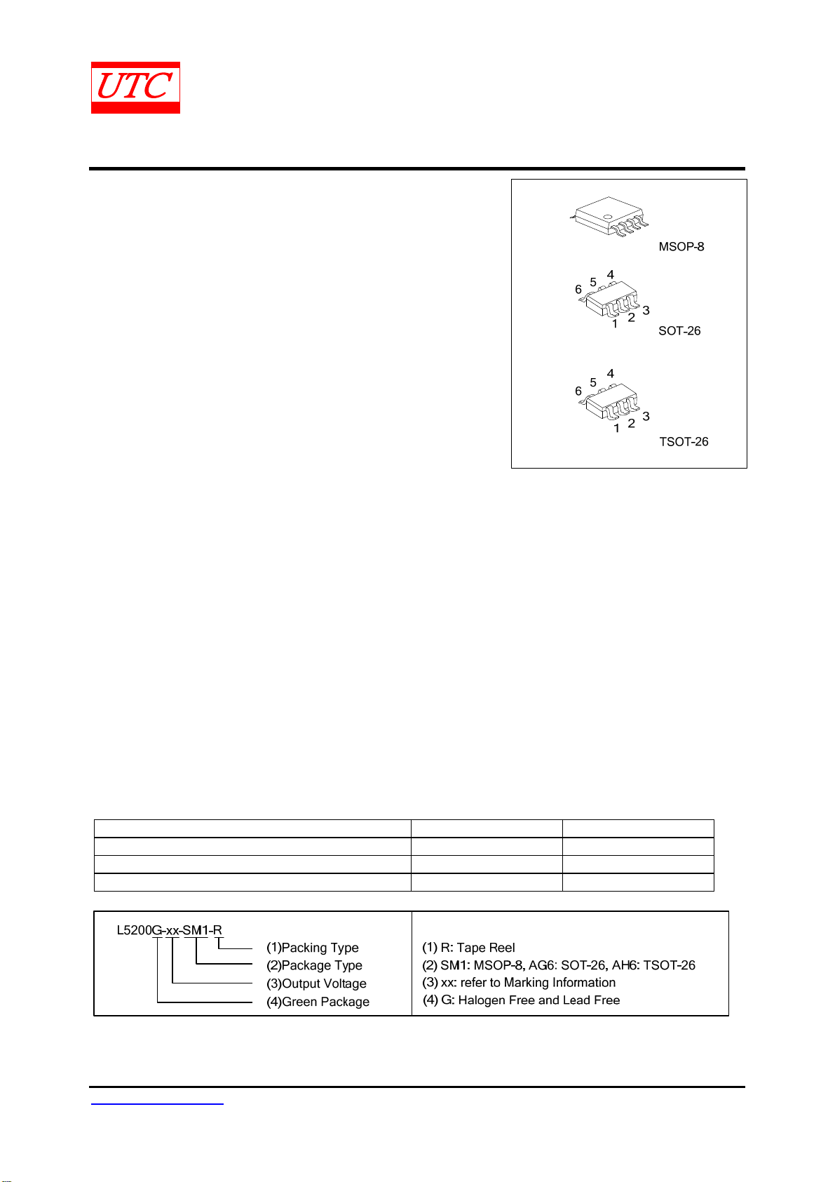
The L5200-ADJ is available in MSOP-8 package and
L5200-fixed in SOT-26 and TSOT-26 package.
IN
during
IN
OUT
and
CMOS IC
FEATURES
* Low Noise Constant Frequency Operation
* Output Current: 100mA
* 2MHz Switching Frequency
* 4.5V/5.0V Fixed Output Voltage
* V
Range: 2.7V ~ V
IN
* Automatic Soft-Start.
* No Inductors
* Less than 1μA of Shutdown Current
OUT
ORDERING INFORMATIO N
Ordering Number Package Packing
L5200L-AD-SM1-R MSOP-8 Tape Reel
L5200L-45-AG6-R SOT-26 Tape Reel
L5200L-50-AH6-R TSOT-26 Tape Reel
Note: xx: Output Voltage, Refer to Marking Information
www.unisonic.com.tw 1 of 7
Copyright © 2014 Unisonic Technologies Co., Ltd QW-R502-029.E
L5200
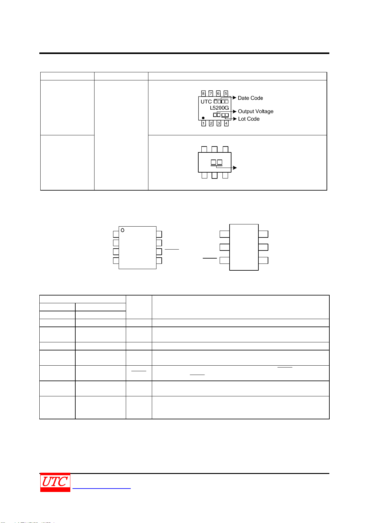
MARKING INFORMATION
PACKAGE VOLTAGE CODE MARKING
MSOP-8
CMOS IC
45: 4.5V
50: 5.0V
AD :ADJ
SOT-26
6
LE G
TSOT-26
PIN CONFIGURATIONS
MSOP-8
C
V
C
PGND
+
IN
-
1
2
3
L5200-ADJ
4
UTC
8
7
6
5
OUT
V
FB
SHDN
SGND
V
GND
SHDN
PIN DESCRIPTION
PIN NO.
L5200-ADJ L5200-xx
MSOP-8 SOT-26/TSOT-26
1 6 C+ Flying Capacitor Positive Terminal
2 5 VIN
3 4 C¯ Flying Capacitor Negative Terminal
4, 5 2 GND
6 3
7 X FB
8 1 V
X : The pin is Inexistent for SOT-26 and TSOT-26 package.
PIN
NAME
SHDN
OUT
Input Supply Voltage, should be bypassed with a 1μF~4.7μf low ESR
ceramic capacitor.
Ground terminal, should be tied to a ground plane for best
performance
Shutdown Mode, Active-Low Input. A low on
L5200 series.
must not be allowed to float.
SHDN
Feedback Input Pin for Adjustable output. An output divider should be
connected from V
to FB to program the output voltage.
OUT
Regulated Output Voltage, should be bypassed with a 1μF~4.7μF low
ESR ceramic capacitor as close as possible to the pin for best
performance
5
4
21
3
SOT-26/TSOT-26
1
OUT
2
3
FUNCTION
Voltage Code
UTC
L5200-XX
(Fixed)
+
6
C
VIN
5
-
C
4
disables the
SHDN
UNISONIC TECHNOLOGIES CO., LTD 2 of 7
www.unisonic.com.tw QW-R502-029.E
L5200
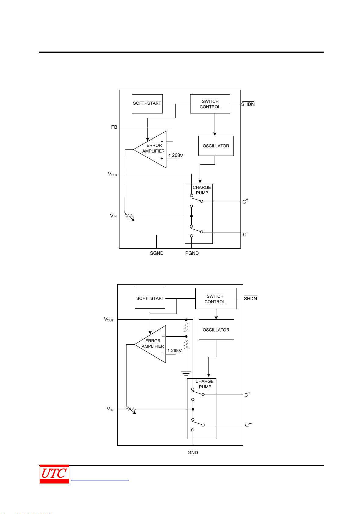
BLOCK DIAGRAM
UTC L5200 Adjustable version (MSOP-8)
CMOS IC
UTC L5200 fixed version (SOT-26/TSOT-26)
UNISONIC TECHNOLOGIES CO., LTD 3 of 7
www.unisonic.com.tw QW-R502-029.E

L5200
CMOS IC
ABSOLUTE MAXIMUM RATINGS
PARAMETER SYMBOL RATINGS UNIT
Input Voltage(to GND) VIN -0.3 ~ 6 V
Charge Pump Voltage(to GND) V
Shutdown Voltage(to GND)
Maximum DC Output Current (Note 1) I
V
Short-Circuit Duration Indefinite
OUT
Operating Temperature T
Storage Temperature T
Notes 1: Based on long-term current density limitations.
2: Stressed above Absolute Maximum Ratings may impair life or cause permanent damage to the device.
3. The device is guaranteed to meet performance specification within 0℃~+70℃ operating temperature range
and assured by design from -20℃~+85℃, characteristic and correlation with static process control.
ELECTRICAL CHARACTERISTICS
-0.3 ~ 5.5 V
OUT
V
SHDN
150 mA
OUT
-20 ~ +85 °C
OPR
-40 ~ +150 °C
STG
-0.3 ~ (V
+0.3) V
IN
(TA =25°C, VIN =3.6V, C
=1μF, CIN=1μF, C
FLY
=1μF, unless otherwise specified.)
OUT
PARAMETER SYMBOL TEST CONDITIONS MIN TYP MAX UNIT
Input Supply Voltage Range VIN *2.7 V
Output Voltage
L5200-4.5V
L5200-5.0V I
V
Shutdown Input Threshold
Feedback Voltage (For L5200-ADJ)
V
Output Ripple Voltage(For L5200-fixed)
Operating Supply Current ICC
Shutdown Current
I
Shutdown Input Current
Feedback Input Current (For L5200-ADJ)
Open-Loop Output Resistance ROL
Switching Frequency F
Efficiency (For UTC L5200-fixed)
Soft Start Time tON
4.41 4.5 4.59 V
OUT
V
*1.3 V
IH
≤100mA * 4.9 5 5.1 V
OUT
VIL * 0.4 V
* 1.217 1.268 1.319 V
FB
VIN=3V, I
V
R
=0mA,
I
OUT
SHDN
SHDN
SHDN
I
IH
SHDN
IIL
VFB=1.4V * -50 50 nA
I
FB
=3V, I
V
IN
V
=0V
FB
(R
≡ (2VIN – V
OL
1 MHz
OSC
V
=3V, I
IN
=3V, I
IN
η V
10%~90%
=100mA 30 mV
OUT
=VIN
=0V, V
=VIN
=0V
OUT
SHDN
=0V
OUT
=100mA
* 1.7 5 mA
* 1 μA
* -1 1 μA
* -1 1 μA
9.2 Ω
)/I
OUT
)
0.8 ms
OUT
=50mA 80 %
OUT
=0mA
OUT
OUT
Note: * stand for specifications which apply over the designed operating temperature range.
V
P-P
UNISONIC TECHNOLOGIES CO., LTD 4 of 7
www.unisonic.com.tw QW-R502-029.E

L5200
TYPICAL APPLICATION CIRCUIT
CMOS IC
UNISONIC TECHNOLOGIES CO., LTD 5 of 7
www.unisonic.com.tw QW-R502-029.E

L5200
TYPICAL CHARACTERISTICS (L5200-5.0V)
CMOS IC
)
V
(
e
g
a
t
l
o
V
t
u
p
t
u
O
)
V
(
e
g
a
t
l
o
V
t
u
p
t
u
O
No Load Supply Current vs Supply Voltage
6
CIN = COUT = CFLY = 1μF
VSHDN = VIN
5
4
3
2.7
Ta = 85℃
3.0 3.3 3.6 3.9
Ta = 25℃
Ta = -40℃
Supply Voltage (V)
4.2
4.5
Oscillator Frequency vs Supply Voltage
3.0
2.8
2.6
2.4
2.2
2.0
1.8
1.6
1.4
1.2
1.0
Ta = -40℃
2.7
3.0 3.3 3.6 3.9
Supply Voltage (V)
Ta = 25℃
Ta = 85℃
4.2
4.5
UNISONIC TECHNOLOGIES CO., LTD 6 of 7
www.unisonic.com.tw QW-R502-029.E

L5200
TYPICAL CHARACTERISTICS (L5200-5.0V) (cont.)
CMOS IC
VOUT (AC
COUPLED)
20mV/DIV
OUT = 1μF
C
C
OUT = 3.3μF
COUT = 10μF
V
IN = 3.3V
L = 100mA
I
Output Ripple
200ns/DIV
10mA ~ 90mA
(AC COUPLED)
50mA/DIV
VOUT
50mV/DIV
L
I
V
IN = 3.3V
COUT = 1μF
Load Transient Response
10μs/DIV
UTC assumes no responsibility for equipment failures that result from using products at values that
exceed, even momentarily, rated values (such as maximum ratings, operating condition ranges, or
other parameters) listed in products specifications of any and all UTC products described or contained
herein. UTC products are not designed for use in life support appliances, devices or systems where
malfunction of these products can be reasonably expected to result in personal injury. Reproduction in
whole or in part is prohibited without the prior written consent of the copyright owner. The information
presented in this document does not form part of any quotation or contract, is believed to be accurate
and reliable and may be changed without notice.
UNISONIC TECHNOLOGIES CO., LTD 7 of 7
www.unisonic.com.tw QW-R502-029.E

 Loading...