

UNISONIC TECHNOLOGIES CO., LTD
L1186
CMOS IC
600mA CMOS LDO
DESCRIPTION
The UTC L1186 is a COMS positive linear regulator. One of its
features is the very low quiescent current typical as low as 30μA and
its dropout voltage is extremely low with 600mA output current.
The internal circuit includes thermal shutdown and current
fold-back to prevent device failure when the circuit is operated in the
bad conditions.
In application, the UTC L1186 needs a low noise, regulated
supply. For stable operation, the output capacitance value should be
2.2μF or more.
The UTC L1186 is an ideal for battery applications, such as
instrumentations, portable electronics, wireless devices, cordless
phones, PC peripherals, and battery powered widgets.
FEATURES
* Accurate to Within 1.5%
* Quiescent Current: 30μA
* Internal Over-Temperature Shutdown
* With Current Limiting
* Internal Short Circuit Current Fold-Back
* With Noise Reduction Bypass Capacitor
* Has Power-Saving Shutdown Mode
* Very Low Temperature Coefficient
4
5
3
2
1
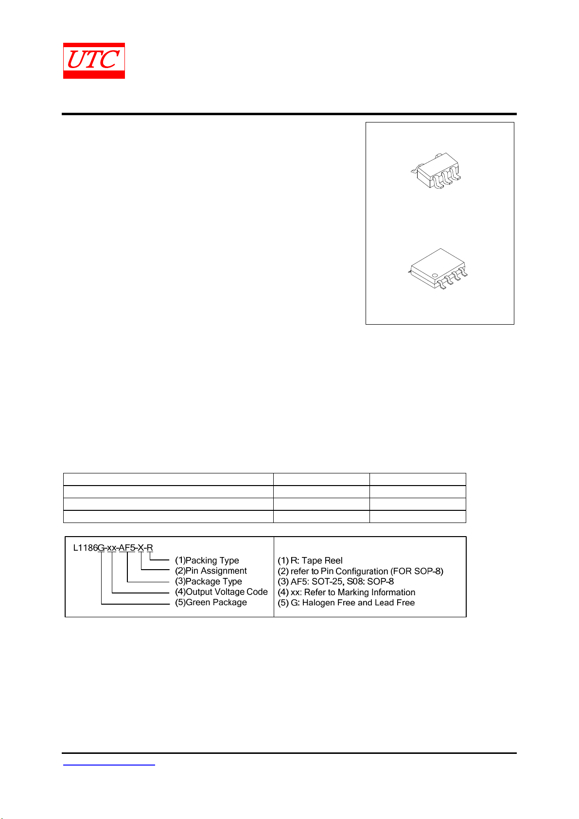
SOT-25
1
SOP-8
ORDERING INFORMATION
Ordering Number Package Packing
L1186G-xx-AF5-R SOT-25 Tape Reel
L1186G-xx-S08-A-R SOP-8 Tape Reel
L1186G-xx-S08-B-R SOP-8 Tape Reel
Note: xx: Output Voltage, refer to Marking Information.
www.unisonic.com.tw 1 of 7
Copyright © 2015 Unisonic Technologies Co., Ltd QW-R502-319.I
L1186 CMOS IC
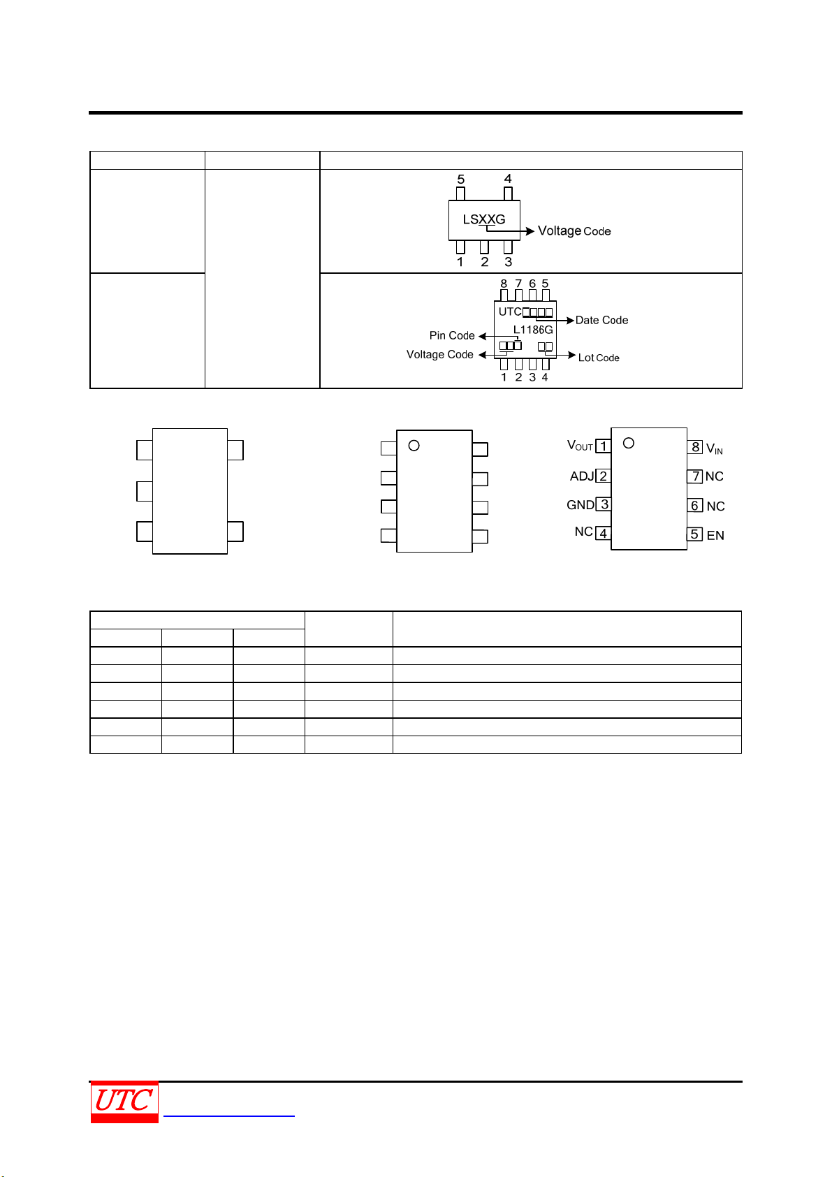
MARKING INFORMATION
PACKAGE VOLTAGE CODE MARKING
SOT-25
AD: ADJ
SOP-8
PIN CONFIGURATION
V
GND
GND
EN
IN
1
2
3
4
8
7
6
5
V
GND
EN
1
IN
2
3
V
5
OUT
ADJ
4
SOT-25 SOP-8(A) SOP-8(B)
PIN DESCRIPTION
PIN NO
SOT-25 SOP-8(A) SOP-8(B)
1 1 8 VIN Input for voltage input.
2 2, 3, 6, 7 3 GND Ground.
3 4 5 EN Enable pin.
4 5 2 ADJ Adjusted Voltage
5 8 1 V
- - 4, 6, 7 NC No connection
PIN NAME DESCRIPTION
Output voltage pin
OUT
V
OUT
GND
GND
ADJ
UNISONIC TECHNOLOGIES CO., LTD 2 of 7
www.unisonic.com.tw QW-R502-319.I
L1186 CMOS IC
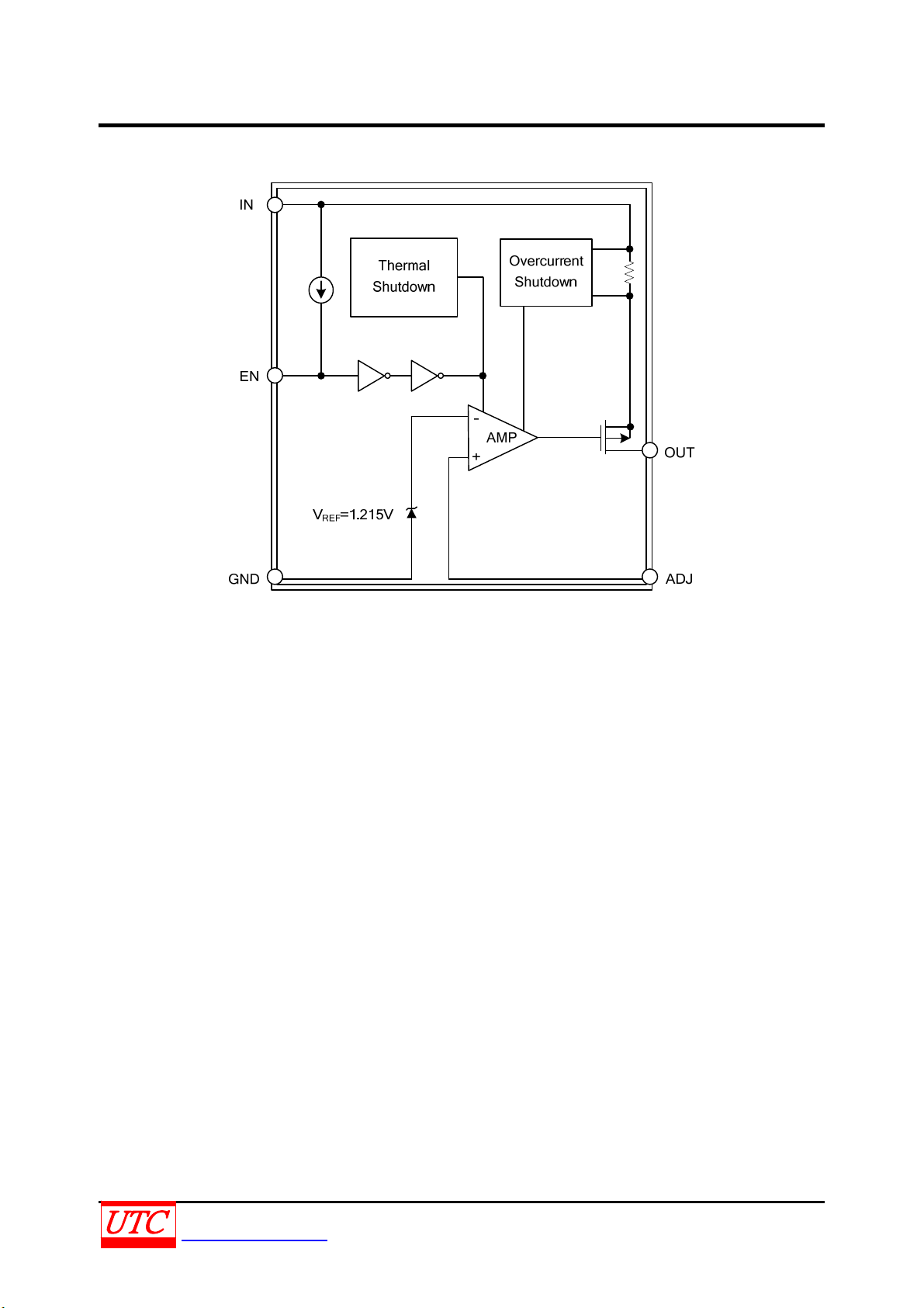
BLOCK DIAGRAM
UNISONIC TECHNOLOGIES CO., LTD 3 of 7
www.unisonic.com.tw QW-R502-319.I

L1186 CMOS IC
ABSOLUTE MAXIMUM RATING (T
= 25°C, unless otherwise specified.)
A
PARAMETER SYMBOL RATINGS UNIT
Input Voltage VIN 8 V
Output Voltage V
Output Current I
Power Dissipation
SOT-25 400
SOP-8
GND-0.3 ~ VIN+0.3 V
OUT
P
D
OUT
PD
OUTIN
V-V
600
A
mW
Junction Temperature TJ 150 °C
Operating Temperature T
Storage Temperature T
-40~+85 °C
OPR
-65~+150 °C
STG
Note: Absolute maximum ratings are those values beyond which the device could be permanently damaged.
Absolute maximum ratings are stress ratings only and functional device operation is not implied.
THERMAL RESISTANCES CHARACTERISTICS
PARAMETER SYMBOL RATINGS UNIT
Junction to Ambient
Junction to Case (Note)
Note: θJC on center of molding compound if IC has on tab.
SOT-25 260
SOP-8
SOT-25 81
SOP-8
θJA
θJC
200
65
°C/W
°C/W
UNISONIC TECHNOLOGIES CO., LTD 4 of 7
www.unisonic.com.tw QW-R502-319.I

L1186 CMOS IC
ELECTRICAL CHARACTERISTICS (T
= 25°C, unless otherwise specified.)
A
Adjusted Voltage
PARAMETER SYMBOL TEST CONDITIONS MIN TYP MAX UNIT
Input Voltage VIN Note1 7 V
Reference Voltage V
Output Voltage Accuracy V
Line Regulation
Load Regulation
Output Current I
Current Limit I
Short Circuit Current ISC V
Adjusted Current I
Ground Pin Current I
Dropout Voltage VD
1.196 1.215 1.234 V
REF
I
OUT
OUT
V∆
OUT
V
V∆
OUT
OUT
V
V
OUT
V
LIMIT
I
ADJ
I
GND
=1mA -1.5 1.5 %
OUT
+2
1.4V<V
2.0V<V
1.4V<V
2.0V<V
I
=1mA
OUT
V
I
OUT
OUT
OUT
I
OUT
V
IN=VOUT
OUT
OUT
OUT
OUT=VO(NOM)
+1~V
OUT
=1mA~600 mA 0.2 1 %
>1.3V 600 mA
>1.3V 600 800 mA
<0.8V 300 600 mA
=0mA 30 50 μA
=1mA~600mA 35 μA
=600mA
-2.0%
≤2.0V -0.15 0.15 %
OUT
<4.0V -0.1 0.02 0.1 %
OUT
≤2.0V 1400 mV
O(NOM)
≤2.8V 800 mV
O(NOM)
Over Temperature Shutdown OTS 150 °C
Over Temperature Hysteresis OTH 30 °C
Temperature Coefficient of
Output Voltage
Power Supply Rejection PSRR
Output Voltage Noise eN
EN Input Threshold
EN Input Bias Current
T
30
CVO
=100mA
I
OUT
C
=2.2μF ceramic
OUT
C
=0.01μF
BYP
f=10Hz~100kHz, I
C
=2.2μF , C
OUT
VEH VIN=2.7V~7V 2.0 V
V
VIN=2.7V~7V 0 0.4 V
EL
IEH VEN=VIN, VIN=2.7V~7V 0.1 μA
I
VEN=0V, VIN=2.7V~7V 0.5 μA
EL
Shutdown Supply Current ISD VIN=5V, V
f=1kHz 40 dB
f=10kHz 20 dB
f=100kHz 15 dB
=10mA
OUT
=0.1μF
BYP
=0V, VEN<VEL 0.5 1 μA
OUT
30 μVrms
ppm/°
C
V
IN
PG Leakage Current ILC VPG=7V 1 μA
Notes: 1. V
IN(MIN)=VOUT+VD
2. To prevent the Short Circuit Current protection feature from being prematurely activated, the input voltage
must be applied before a current source load is applied.
UNISONIC TECHNOLOGIES CO., LTD 5 of 7
www.unisonic.com.tw QW-R502-319.I

L1186 CMOS IC
TYPICAL APPLICATION CIRCUIT
Adjusted Voltage
EN
IN
+
V
= 1.215 ( R1/R2 +1 )
OUT
C2 is unnecessary if R1 or R2 < 20 K
R
and R2use resistance value within 1% accuracy for correct for correct V
1
C1
1µF
EN
IN
GND
OUT
ADJ
R1
R2
C2
100p
OUT
C3
2.2µF
OUT
UNISONIC TECHNOLOGIES CO., LTD 6 of 7
www.unisonic.com.tw QW-R502-319.I

L1186 CMOS IC
TYPICAL CHARACTERISTICS
IN
V
OUT
V
(10mV/DIV)
O
I
(2V/DIV)
(500mA/DIV)
UTC assumes no responsibility for equipment failures that result from using products at values that
exceed, even momentarily, rated values (such as maximum ratings, operating condition ranges, or
other parameters) listed in products specifications of any and all UTC products described or contained
herein. UTC products are not designed for use in life support appliances, devices or systems where
malfunction of these products can be reasonably expected to result in personal injury. Reproduction in
whole or in part is prohibited without the prior written consent of the copyright owner. The information
presented in this document does not form part of any quotation or contract, is believed to be accurate
and reliable and may be changed without notice.
UNISONIC TECHNOLOGIES CO., LTD 7 of 7
www.unisonic.com.tw QW-R502-319.I

 Loading...