

UNISONIC TECHNOLOGIES CO., LTD
2N7002
Power MOSFET
0.3A, 60V N-CHANNEL
POWER MOSFET
DESCRIPTION
The UTC 2N7002 uses advanced technology to provide
excellent R
voltages. This device is suitable for use as a load switch or in PWM
applications.
FEATURES
* High Density Cell Design for Low R
* Voltage Controlled Small Signal Switch
* Rugged and Reliable
* High Saturation Current Capability
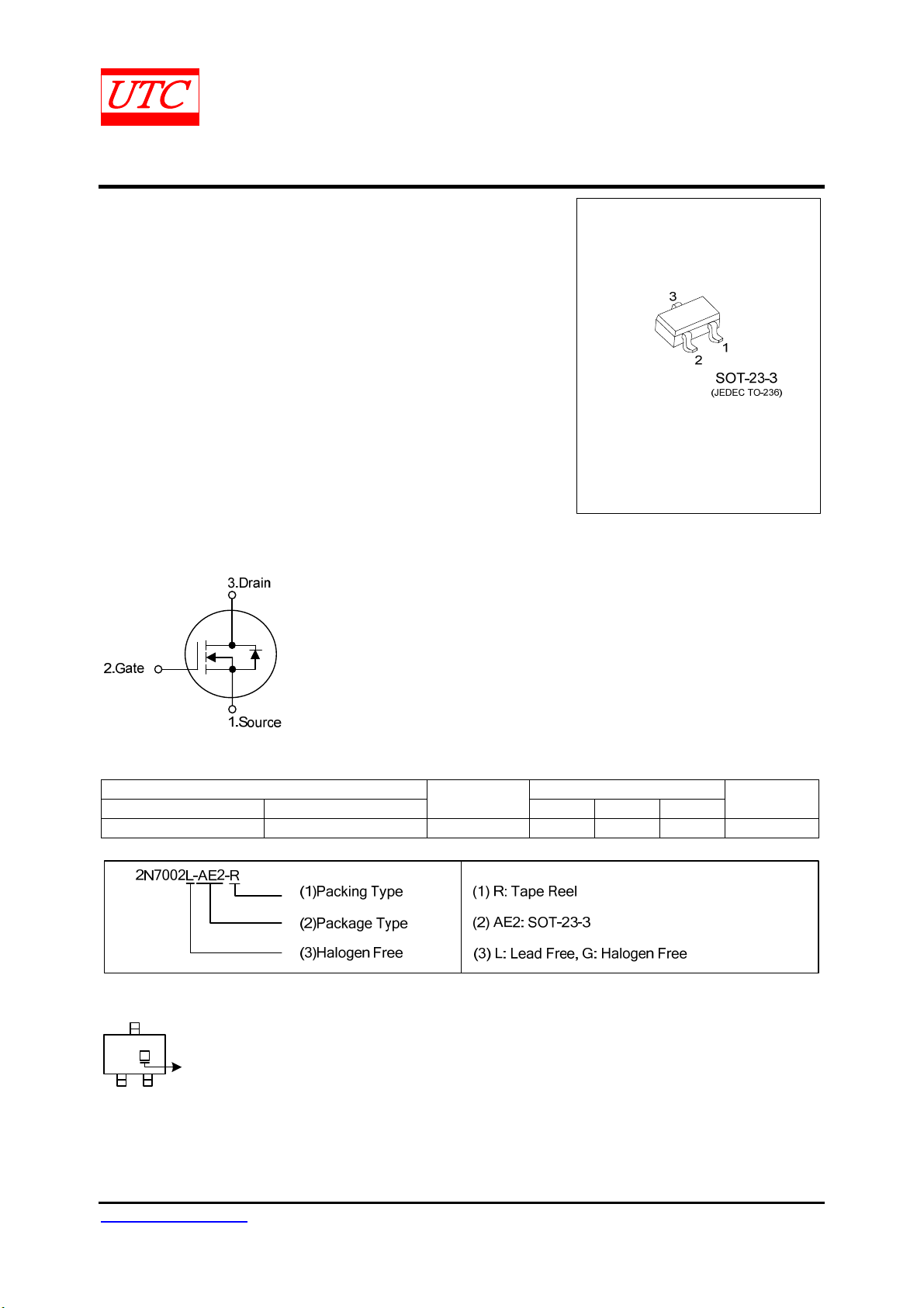
SYMBOL
, low gate charge and operation with low gate
DS(ON)
.
DS(ON)
ORDERING INFORMATION
Ordering Number
Lead Free Halogen Free 1 2 3
2N7002L-AE2-R 2N7002G-AE2-R SOT-23-3 S G D Tape Reel
MARKING
3P
L: Lead Free
G: Halogen Free
Package
Pin Assignment
Packing
www.unisonic.com.tw 1 of 6
Copyright © 2013 Unisonic Technologies Co., Ltd QW-R203-037, L
2N7002 Power MOSFET
ABSOLUTE MAXIMUM RATINGS (T
=25°C, unless otherwise specified.)
A
PARAMETER SYMBOL RATINGS UNIT
Drain-Source Voltage V
Drain-Gate Voltage (R
Gate Source Voltage
Drain Current
≤1MΩ) V
GS
Continuous
Non Repetitive(tP<50μs) ±40
Continuous
Pulsed 800
Power Dissipation
Derated Above 25°C 1.6 mW/°C
60 V
DSS
60 V
DGR
V
GSS
ID
PD
±20
300
V
mA
200 mW
Junction Temperature TJ + 150 °C
Storage Temperature T
-55 ~ +150 °C
STG
Note: Absolute maximum ratings are those values beyond which the device could be permanently damaged.
Absolute maximum ratings are stress ratings only and functional device operation is not implied.
THERMAL DATA
PARAMETER SYMBOL RATINGS UNIT
Junction to Ambient θJA 625 °C/W
Junction to Case θJC 215 °C/W
ELECTRICAL CHARACTERISTICS (T
PARAMETER SYMBOL TEST CONDITIONS MIN TYP MAX UNIT
OFF CHARACTERISTICS
Drain-Source Breakdown Voltage BV
Drain-Source Leakage Current I
Gate-Source Leakage Current
ON CHARACTERISTICS
(Note)
Gate Threshold Voltage V
Drain-Source On-Voltage V
Static Drain-Source On-Resistance R
DSS
VDS=60V, VGS =0V 1 μA
DSS
I
V
GSSF
I
VGS =-20V, VDS=0V -100 nA
GSSR
GS(TH)
DS (ON)
DS (ON)
DYNAMIC CHARACTERISTICS
Input Capacitance C
Output Capacitance C
Reverse Transfer Capacitance C
VDS=25V,VGS=0V,f=1.0MHz 20 50 pF
ISS
11 25 pF
OSS
4 5 pF
RSS
Turn-On Time tON
Turn-Off Time t
OFF
DRAIN-SOURCE DIODE CHARACTERISTICS AND MAXIMUM RATINGS
Drain-Source Diode Forward Voltage VSD VGS=0V, Is=300mA (Note) 0.88 1.5 V
Maximum Pulsed Drain-Source Diode
Forward Current
Maximum Continuous Drain-Source
Diode Forward Current
I
0.8 A
SM
I
300 mA
S
Note: Pulse Test: Pulse Width≤300μs, Duty Cycle≤2.0%
=25°C, unless otherwise specified)
A
VGS=0V, ID=10μA 60 V
=20V, VDS=0V 100 nA
GS
VGS = VDS, ID=250μA 1 2.1 2.5 V
V
= 10V, ID=300mA 0.6 3.75
GS
VGS = 5.0V, ID=50mA 0.375
V
=10V, ID=300mA 7.5 Ω
GS
VGS =5.0V, ID=50mA 7.5 Ω
V
=30V, RL=150Ω, ID=200mA,
DD
V
=10V, R
GS
V
=30V, RL=25Ω, ID=200mA,
DD
V
=10V, R
GS
GEN
GEN
=25Ω
=25Ω
20 nS
20 nS
V
UNISONIC TECHNOLOGIES CO., LTD 2 of 6
www.unisonic.com.tw QW-R206-037,L
2N7002 Power MOSFET
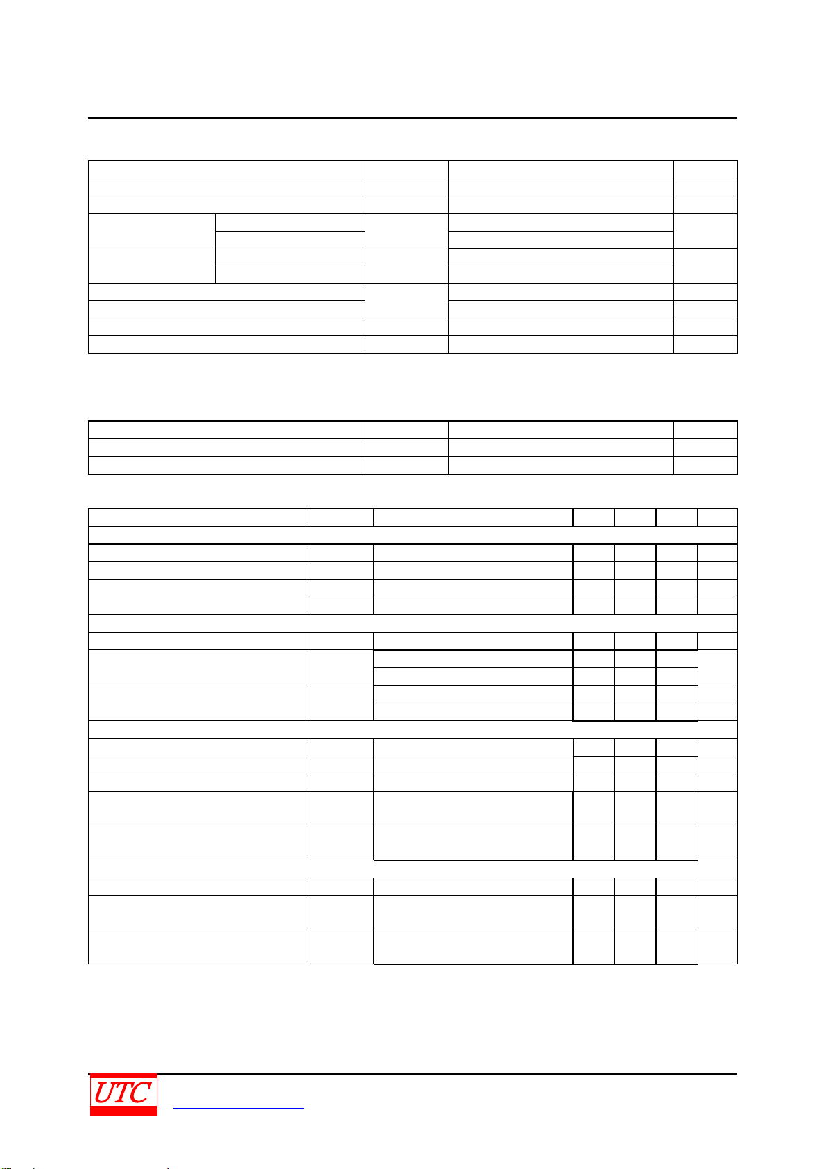
TEST CIRCUIT AND WAVEFORM
V
DD
R
L
V
IN
V
D
V
GS
R
GEN
DUT
G
S
OUT
Fig. 1
t
D(ON)
Output, V
OUT
t
ON
t
R
t
D(OFF)
90%
10%10%
t
OFF
90%
t
F
Inverted
90%
Input, V
IN
50%50%
10%
Pulse Width
Fig. 2 Switching Waveforms
UNISONIC TECHNOLOGIES CO., LTD 3 of 6
www.unisonic.com.tw QW-R206-037,L
2N7002 Power MOSFET
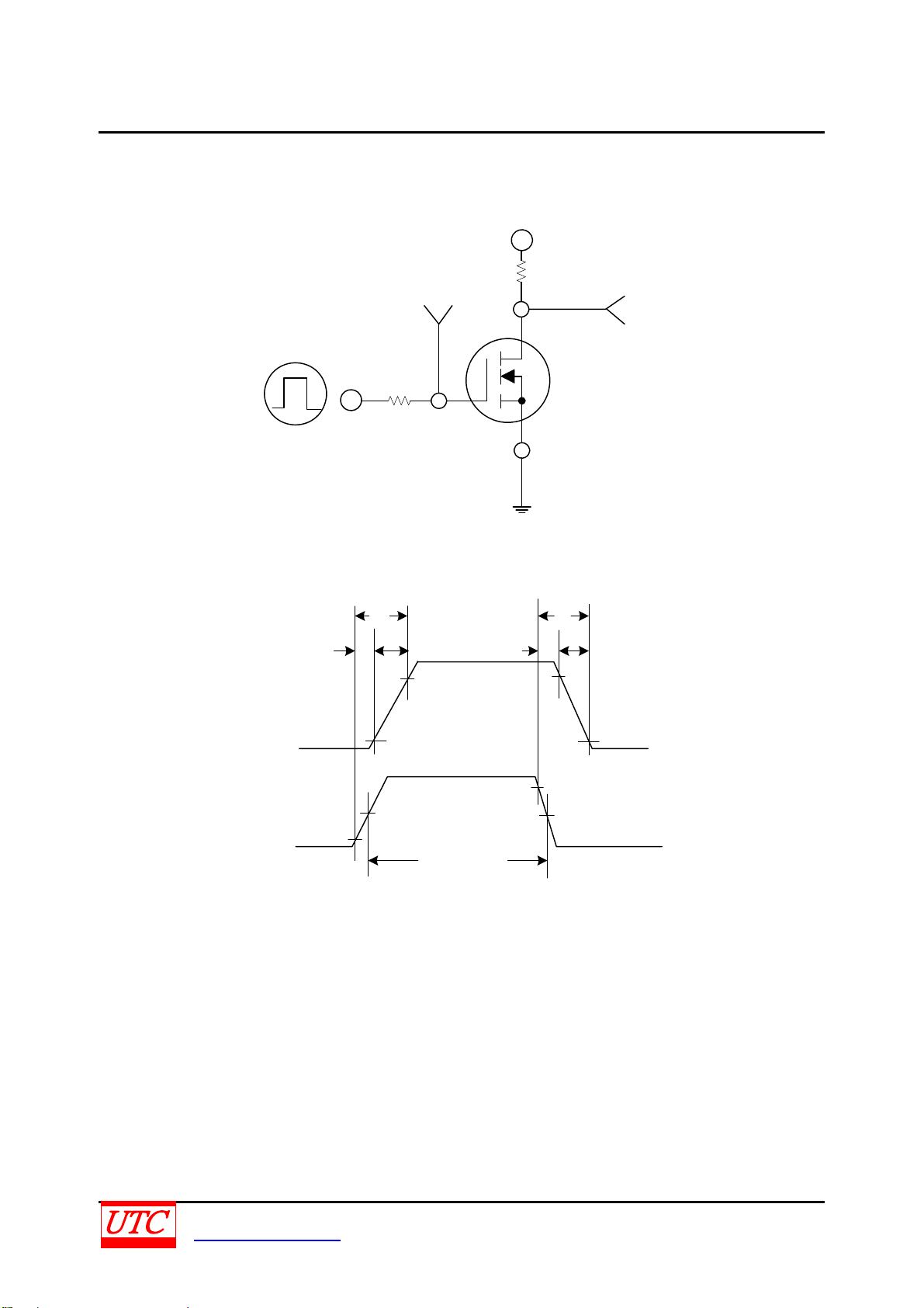
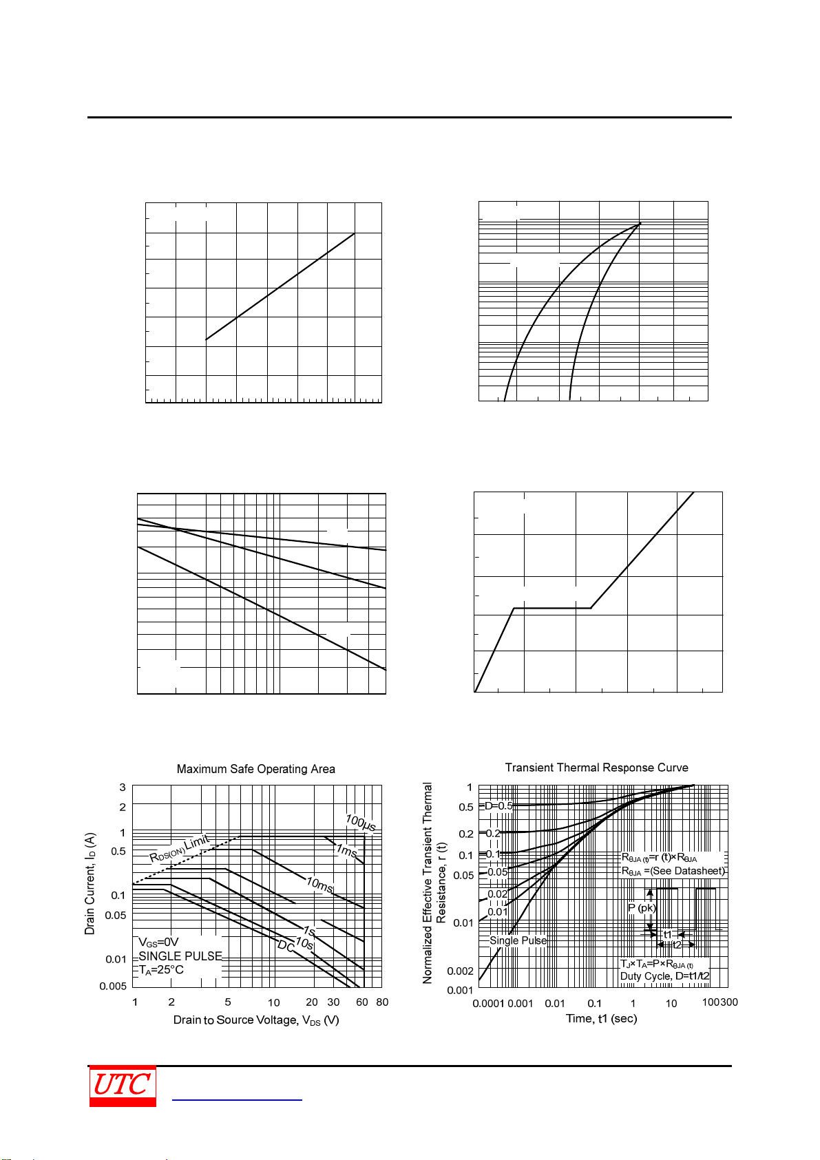
TYPICAL CHARACTERISTICS
(A)
D
Drain-Source Current, I
Normalized Drain-Source
1.75
(Ω)
DS(ON)
1.25
ON- Resistance, R
0.75
On-Resistance Varisation with Temperature
2
VGS=10V
I
=300mA
D
1.5
1
Normalized Drain-Source
(Ω)
DS (ON)
ON-Resistance, R
3
2.5
(Ω)
2
DS (ON)
1.5
1
Resistance, R
0.5
Normalized Drain-Source ON-
On-Resistance Varisation with Drain
Current and Temperature
=10V
V
GS
TJ=125°C
25°C
0.5
-
50
-
25
25
0
Junction Temperature, TJ(°C)
50
10075
125
150
0
0
0.4
0.8
Drain Current,ID(A)
(A)
D
Drain Current, I
(V)
GS(TH)
Voltage, V
Normalized Gate-Source Threshold
UNISONIC TECHNOLOGIES CO., LTD 4 of 6
www.unisonic.com.tw QW-R206-037,L
1.61.2
2
2N7002 Power MOSFET
TYPICAL CHARACTERICS (Cont.)
Body Diode Forward Voltage Varisation
2
VGS=0V
1
0.5
0.1
0.2
with Temperature
TJ =125°C
0.4
Body Diode Forward Voltage, V
25°C
0.6
Gate Charge Characteristics
10
V
= 25V
DS
8
6
ID = 300mA
4
2
0
0
0.4
0.8
Gate Charge, Qg (nC)
0.8
11.2
1.2
SD
1.6
1.4
(V)
2
(V)
DSS
Voltage, BV
Normalized Drain-Source Breakdown
Capacitance (pF)
1.1
1.075
1.05
1.025
0.975
0.95
0.925
60
40
20
10
5
2
1
1
-50
VGS=0V
f=1MHz
1
Breakdown Voltage Varisation
with Temperature
ID = 250μA
-25
25 50
0
Junction Temperature, TJ(°C)
Capacitance Characteristics
3
2
5
10
Drain to Source Voltage, VDS(V)
20
(A)
S
0.0 5
0.01
0.005
Reverse Drain Current, I
0.001
150
125
10075
C
ISS
C
oss
C
RSS
(V)
GS
Gate-Source Voltage, V
5030
UNISONIC TECHNOLOGIES CO., LTD 5 of 6
www.unisonic.com.tw QW-R206-037,L

2N7002 Power MOSFET
UTC assumes no responsibility for equipment failures that result from using products at values that
exceed, even momentarily, rated values (such as maximum ratings, operating condition ranges, or other
parameters) listed in products specifications of any and all UTC products described or contained herein.
UTC products are not designed for use in life support appliances, devices or systems where malfunction
of these products can be reasonably expected to result in personal injury. Reproduction in whole or in
part is prohibited without the prior written consent of the copyright owner. The information presented in
this document does not form part of any quotation or contract, is believed to be accurate and reliable
and may be changed without notice.
UNISONIC TECHNOLOGIES CO., LTD 6 of 6
www.unisonic.com.tw QW-R206-037,L

 Loading...