USDIGITAL RED3600, RED3000, RED6, RED5, RED50 Datasheet
...
AC LINE FREQUENCY DIVIDERS
RED SERIES
RED 5/6 Divide by 5 or 6
RED 50/60 Divide by 50 or 60
RED 100/120 Divide by 100 or 120
RED 300/360 Divide by 300 or 360
RED 500/600 Divide by 500 or 600
RED 3000/3600 Divide by 3000 or 3600
FEATURES:
• Clock input pulse shaper accepts 50Hz/60Hz
sine wave directly
• Fully static counter operation
• +4.5V to +15V operation (VDD-VSS)
• Low power dissipation
• High noise immunity
• Reset
• Input Enable
• 50Hz/60Hz division select input
• Output low power TTL compatible at +4.5V operation
• Square Wave Output (except for ÷ 5)
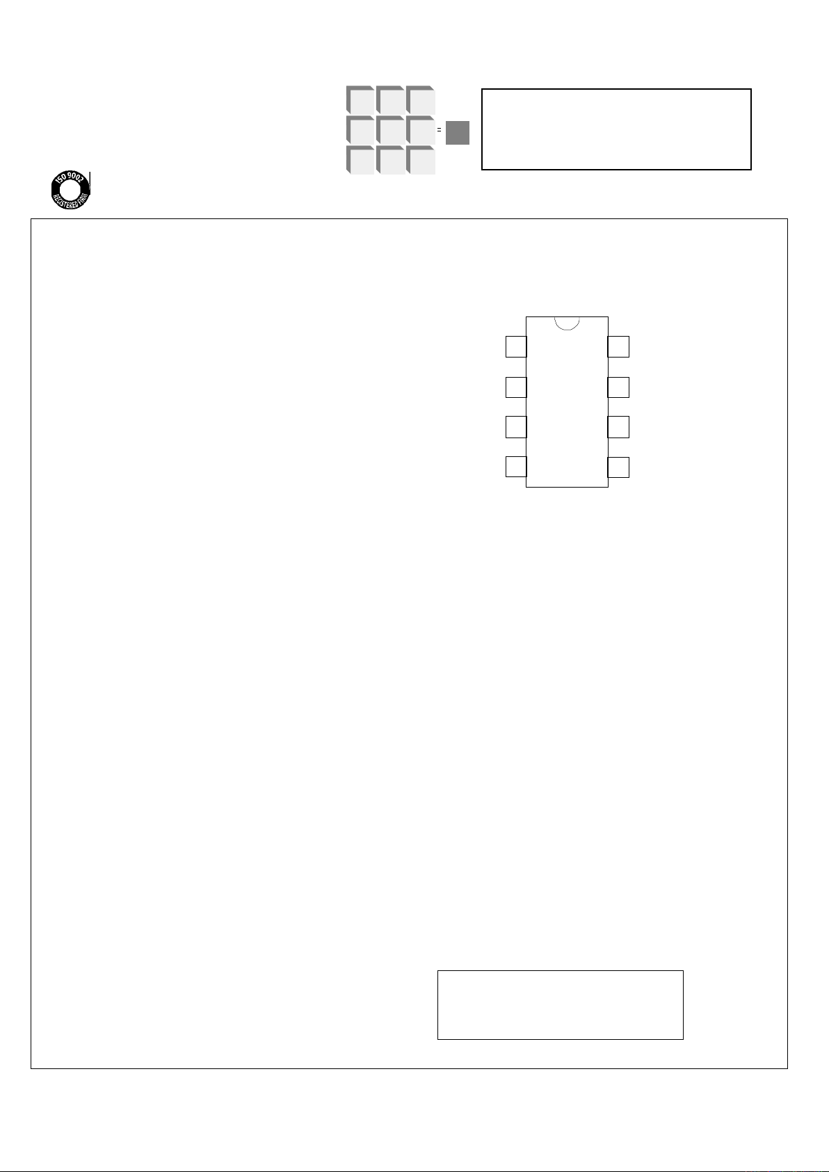
• RED x/y (DIP); RED x/y-S (SOIC) See Figure 1
APPLICATION:
Time base generator from either 50 Hz or 60 Hz line
frequency to produce:
10 pulses per second (RED 5/6)
1 pulse per second (RED 50/60)
1 pulse per 2 seconds (RED 100/120)
1 pulse per .1 minute (RED 300/360)
1 pulse per 10 seconds (RED 500/600)
1 pulse per minute (RED 3000/3600)
DESCRIPTION OF OPERATION:
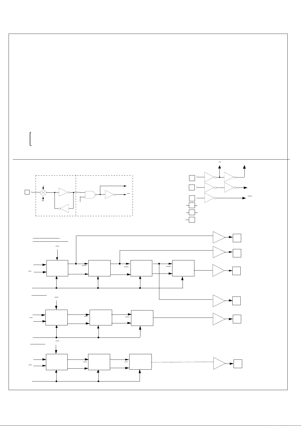
The counter advances by one on each negative transition of the
input clock pulse as long as the Enable signal is High and the
Reset signal is Low. When the Enable signal is Low the input
clock pulses will be inhibited and the counter will be held at the
state it was in prior to bringing the Enable Low. A High Reset
signal clears the counter to zero count.
Depending on the device used, a Low on the Division Select input will cause a Divide by 6, 60, 120, 360, 600 or 3600. A High
on the Division Select will cause a Divide by 5, 50, 100, 300, 500
or 3000.
All outputs are 50% duty cycle except RED 5, where output is
low for two clocks and high for three clocks.
CLOCK INPUT
If input signals are less than the Vss or greater than VDD, a
series input resistor should be used to limit the maximum input
current to 2 mA.
MARKING AS FOLLOWS:
PART MARKING
RED 5/6 RED 6
RED 50/60 RED 60
RED 100/120 RED 120
RED 300/360 RED 360
RED 500/600 RED 600
RED 3000/3600 RED 3600
VDD (V+)
LSI
1
2
3
4
8
7
6
5
OUTPUT
RESET
VSS (-V)
NC
DIVISION SELECT
ENABLE
CLOCK INPUT
PIN ASSIGNMENT - TOP VIEW
FIGURE 1
The information included herein is believed to be
accurate and reliable. However, LSI Computer Systems,
Inc. assumes no responsibilities for inaccuracies, nor for
any infringements of patent rights of others which may
result from its use.
RED-062600-1
LSI/CSI
LSI Computer Systems, Inc. 1235 Walt Whitman Road, Melville, NY 11747 (631) 271-0400 FAX (631) 271-0405
RED SERIES
U
L
®
A3800
July 2000
MAXIMUM RATINGS:
PARAMETER SYMBOL VALUE UNIT
Storage Temperature TSTG -65 to +150 ˚C
Operating Temperature TA -40 to +85 ˚C
DC Supply Voltage (VDD-Vss) +18 V
Voltage at any input VIN Vss -.3 to VDD +.3 V
ENABLE SIGNAL TIMING
If the Enable signal switches Low during a positive clock phase and
then switches High during a negative clock phase, a false count will
be registered. To prevent this from happening, the Enable signal
should not switch Low during a positive clock phase unless the switch
to High also occurs during a positive clock phase. The Enable signal
should normally be switched during a negative clock phase.

ELECTRICAL CHARACTERISTICS: (TA = 25° unless otherwise specified)
TEST CONDITIONS: Vss = OV
Output Capacitance Load = 15 pF
Input Rise and Fall times = 20 ns,
except clock Rise and Fall times
Input Capacitance = 5pF max (any input)
VDD Min Max Units
Quiescent Device Current 5V - 10 uA
10V - 20 uA
Output Voltage, Low Level 5V - 0.0 V
10V - 0.0 V
High Level 5V 4.99 - V
10V 9.99 - V
Clock Input Voltage, Low Level 5V - 1 V
10V - 2 V
High Level 5V 4 - V
10V 8 - V
Input Noise Immunity (except clock) 5V 1.5 - V
(Low and High) 10V 3.0 - V
Output Drive Current
Full N Channel Sink Current 4.5V 0.18 - mA
Temp. (Vout - Vss +.4v) 10V 0.45 - mA
Range
P Channel Sink Current 4.5V 0.3 - mA
(Vout - VDD -1) 10V 0.75 - mA
VDD MIN MAX UNITS
Clock Rise and Fall Time: 5V No Maximum Limit -
10V No Maximum Limit -
Clock Frequency 5V DC 600 KHz
10V DC 1200 KHz
Input Clock Pulse Width 5V 800 - ns
10V 400 - ns
Output Rise and Fall Time 5V - 225 ns
10V - 150 ns
Propagation Delay to Output 5V - 1500 ns
10V - 750 ns
Enable Set-up Time 5V - 300 ns
10V - 150 ns
Reset Pulse Width 5V 800 - ns
10V 400 - ns
Reset Removal Time 5V - 1200 ns
10V - 600 ns
Reset Propagation Delay 5V - 1400 ns
to Output 10V - 700 ns
RED-062600-2
CL IN
CL
CL
R
E
E
5
PULSE SHAPER INPUT CLOCK GENERATOR
6
ENABLE
E
E
2
RESET
R
8
3
4
+4.5V to +15V
GND
N/C
VDD
VSS
7
DIVISION SELECT
DS
3 BIT
JOHNSON
+5/6
3 BIT
JOHNSON
+5/6
3 BIT
JOHNSON
÷10
5 BIT
JOHNSON
÷10
3 BIT
JOHNSON
÷6
5 BIT
JOHNSON
÷10
1 BIT
÷2
CL
CL
CL
CL
D3000/3600
D100/120
RED 5/6,50/60,
300/360,3000/3600
RED 100/120
RED 500/600
R
R
CL2
CL2
CL2
CL2
CL1
CL1
CL1
CL1
CL3
CL3
3 BIT
JOHNSON
+5/6
5 BIT
JOHNSON
÷10
5 BIT
JOHNSON
÷10
CL
CL
D500/600
R
CL2
CL2
CL1
CL1
D5/6
D50/60
D300/360
1
DS
DS
DS
1
1
1
1
1
FIGURE 2. BLOCK DIAGRAM
 Loading...