uPI uP6305AFA9, uP6305AQDD, uP6305ASU8 Schematic [ru]
Preliminary
A
uP6305
1MHz, 2.0A, High-Eefficiency
Synchronous-Rectified Buck Converter
General Description
The uP6305 is a high efficiency synchronous-rectified buck
converter with internal power switches. Fixed 1MHz PWM
operation allows possible smallest output ripple and
external component size. With high conversion efficiency
and small package, the uP6305 is ideally suitable for
portable devices and USB/PCIE-based interface cards
where PCB area is especially concerned.
With internal low R
switches, the uP6305 is capable
DS(ON)
of delivering 2.0A output current over a wide input voltage
range from 2.5V to 5.5V. The output voltage is adjustable
from 0.6V to VIN by a voltage divider. Other features include
internal soft-start, chip enable, overvoltage, under-voltage,
over-temperature and over-current protections. The uP6305
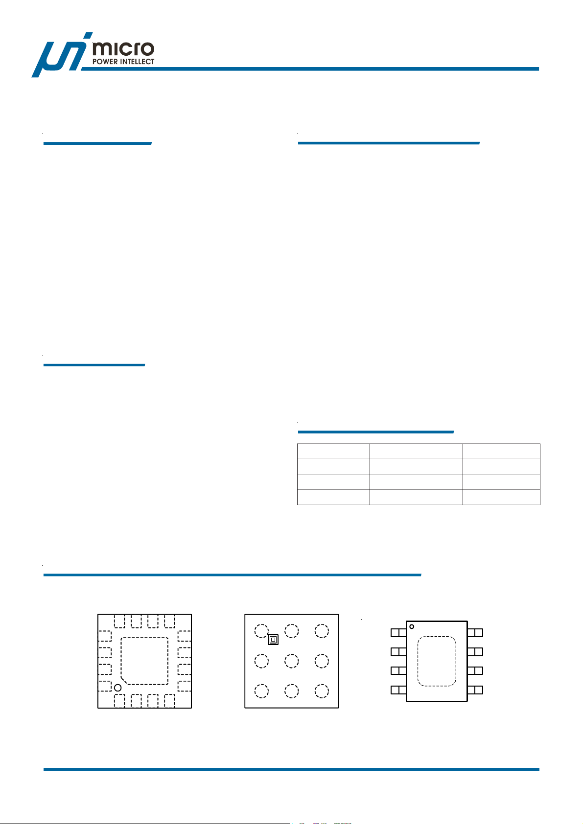
is available in a space-saving WQFN3x3-16L,
WLCSP1.5x1.5-9B or PSOP-8L packages.
Ordering Information
Battery-Powered Portable Devices
MP3 Players
Digital Still Cameras
Wireless and DSL Modems
Personal Information Appliances
802.11 WLAN Power Supplies
FPGA/ASIC Power Supplies
Dynamically Adjustable Power Supply for
CDMA/WCSMA Power Amplifiers
USB-Based xDSL Modems and Other Network
Interface Cards
Point-of-Load Regulation
Features
2.5V to 5.5V Input Voltage Range
Adjustable Output from 0.6V to V
Guaranteed 2.0A Output Current
Accurate Reference: 0.6V (
Up to 95% Conversion Efficiency
Low Quiescent Current
Integrated Low R
MOSFET Switches: 85m
Current Mode PWM Operation
Fixed Frequency: 1MHz
100% Maximum Duty Cycle for Lowest Dropout
Internal Soft-Start
No Schottky Diode Required
Over-Voltage and Under-Voltage Protection
Over-Temperature and Over-Current Protection
WQFN3x3-16L, WLCSP1.5x1.5-9B or PSOP-8L
Upper and Lower
DS(ON)
ΩΩ
Ω and 75m
ΩΩ
IN
+/- +/-
+/- 1.5%)
+/- +/-
ΩΩ
Ω
ΩΩ
Packages
RoHS Compliant and 100% Lead (Pb)-Free
pplications
rebmuNredrOepyTegakcaPkrameR
DDQA5036PuL61-3x3NFQW
9AFA5036PuB9-5.1x5.1PSCLW
8USA5036PuL8-POSP
Note: uPI products are compatible with the current IPC/
JEDEC J-STD-020 requirement. They are halogen-free,
RoHS compliant and 100% matte tin (Sn) plating that are
suitable for use in SnPb or Pb-free soldering processes.
VIN
VIN
VIN
12
11
LX
13
LX
15
LX
15
NC
16
Rev. P00, File Name: uP6305-DS-P0002
PGND
1
2
PGND
PGND
WQFN3x3-16L
VCC
9
10
POK
8
EN
7
NC
6
AGND
5
3
4
FB
PGND
EN VIN VIN
A
NC LX LX
B
GNDFB
C
123
WLCSP1.5x1.5-9B
GND
AGND
EN
POK
Pin Configuration
1
2
GND
3
45
PSOP - 8
FB
8
PGNDNC
7
LX
6
VIN
1uPI Semiconductor Corp., http://www.upi-semi.com
Preliminary
n
uP6305
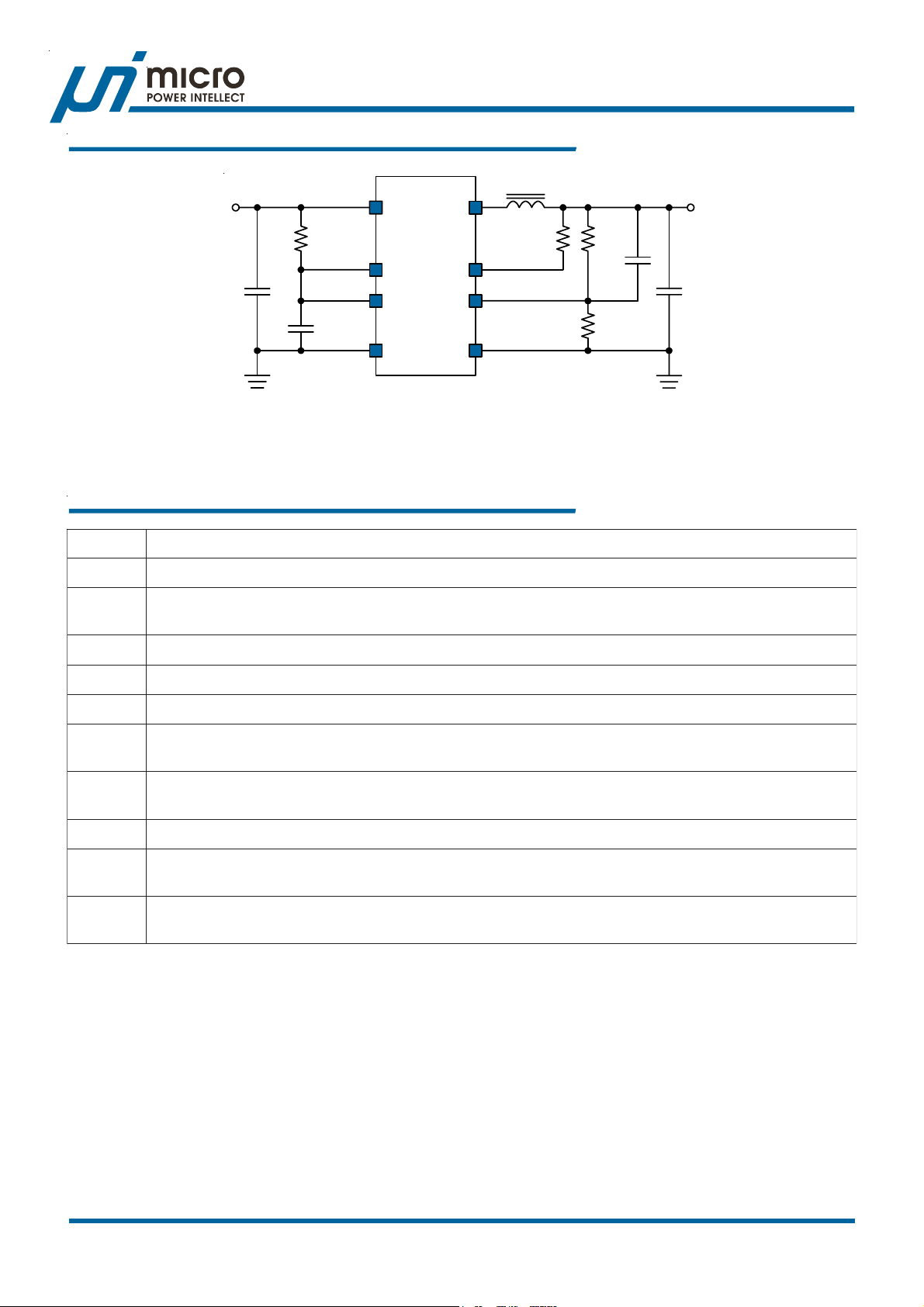
Typical Application Circuit
V
IN
R3
C3
VIN
VCC
EN
uP6305AQDD
PGND
LX
POK
FB
AGND
R2
Option
R1
V
OUT
Functional Pin Descriptio
emaNniPnoitcnuFniP
DNGP
BF
.dnuorGrewoP .nrutersroticapactupnidnatuptuoehtottcennoC
.tupnIkcabdeeF hguorhttuptuorehctiwsehtsesnesBF.reifilpmarorreehtfotupnignitrevniehtsinipsihT
.krowtenredividrotsiserlanretxena
DNGA
CN
NE
CCV
NIV
XL
KOP
desopxE
daP
.dnuorGlangiS .nipsihtotstenenopmoclangisllamsllafonruterehttcennoC
.detcennoCyllanretnItoN
elbanEpihC .retrevnocehtnwodstuhswolcigoL.)hgiHevitcA(
.ylppuSsaiB htiwretlifssapwolaivrewoptupniottcennoC.yrtiucriclanretniehtrofrewopseilppuS
.PAFB5036PurofNIVotdetcennocyllanretnisinipsihT.DNGAotgnilpuoced
.tupnIylppuSrewoP lanretniehtsrewopdnaegatlovtuptuoehtottnerrucseilppustahtegatlovtupnI
.roticapaccimarecR7XroR5XFu01muminimahtiwegatlovtupniehtssapyB.tiucriclortnoc
.tuptuOsehctiwSlanretnI .rotcudnituptuoehtotsnipesehttcennoC
)ylnODDQA5036Pu(noitacidnIKOrewoP ondnadnetratstfosretfaecnadepmihgihtessinipsihT.
.sruccotluaf
.dnuorGrewoP enalpdnuorgotsaivelpitlumhtiwBCPotderedlosllewebdluohsdapdesopxeehT
.ecnamrofreplamrehtlamitporof
Rev. P00, File Name: uP6305-DS-P0002
2uPI Semiconductor Corp., http://www.upi-semi.com
Preliminary
uP6305
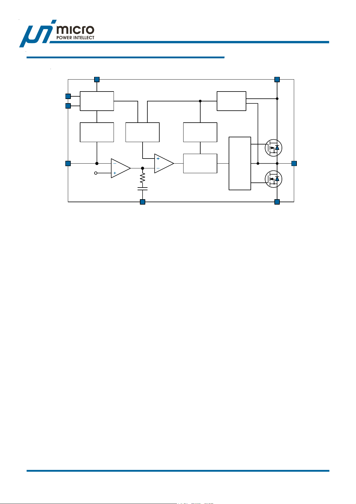
Functional Block Diagram
EN
POK
FB
VCC
OSC &
Shutdown
Control
Over/Under
Voltage
Protection
0.6V
V
REF
VIN
Current
Sense
Slope
Comp.
AGND PGND
Current Limit
Detector
Control Logic Driver
LX
Rev. P00, File Name: uP6305-DS-P0002
3uPI Semiconductor Corp., http://www.upi-semi.com
Preliminary
uP6305
Functional Description
The uP6305 is a high efficiency synchronous-rectified buck
converter with internal power switches. Fixed 1.0MHz PWM
operation allows possible smallest output ripple and
external component size. With high conversion efficiency
and small package, the uP6305 is ideally suitable for
portable devices and USB/PCIE-based interface cards
where PCB area is especially concerned.
With internal low R
switches, the uP6305 is capable
DS(ON)
of delivering 2.0A output current over a wide input voltage
range from 2.5V to 5.5V. The output voltage is adjustable
from 0.6V to VIN by a voltage divider. Other features include
internal soft-start, chip enable, overvoltage, under-voltage,
over-temperature and over-current protections. The uP6305
is available in a space-saving WQFN3x3-16L,
WLCSP1.5x1.5-9B or PSOP-8L packages.
Input Supply Voltages, VIN & V
CC
The uP6305 features seperate power supply and ground
pins for power stages and control circuit, isolating the
control circuit from noise associated with the power
MOSFET switching.
The VIN pins provide current to the power stage. The supply
voltage range is from 2.5V to 5.5V. The uP6305 draws
pulsed current with sharp edges from VIN each time the
upper switch turns on, resulting in voltage ripples and spikes
at supply input. A minimum 10uF ceramic capacitor with
shortest PCB trace is highly recommended for bypassing
the supply input.
The VCC pin provides currents for the internal control circuit.
A power on reset (POR) continuously monitors the input
supply voltage. The POR level is typically 2.3V at VCC rising.
Use low pass filter R3 and C3 as shown in the Typical
Application Circuit to filter the input noise associated with
the power switching.
Chip Enable/Disable and Soft Start
The uP6305 features an EN pin for enable/disable control
of the output voltage. Pulling the EN pin lower than 0.4V
shuts down the uP6305 and reduces its quiescent current
lower than 1uA. In the shutdown mode, both upper and
lower switches are turned off.
Pulling EN pin higher than 1.5V enables the uP6305 and
initiates the softstart cycle once the VCC POR is granted.
The inductor current is limited to fractions of its rated value
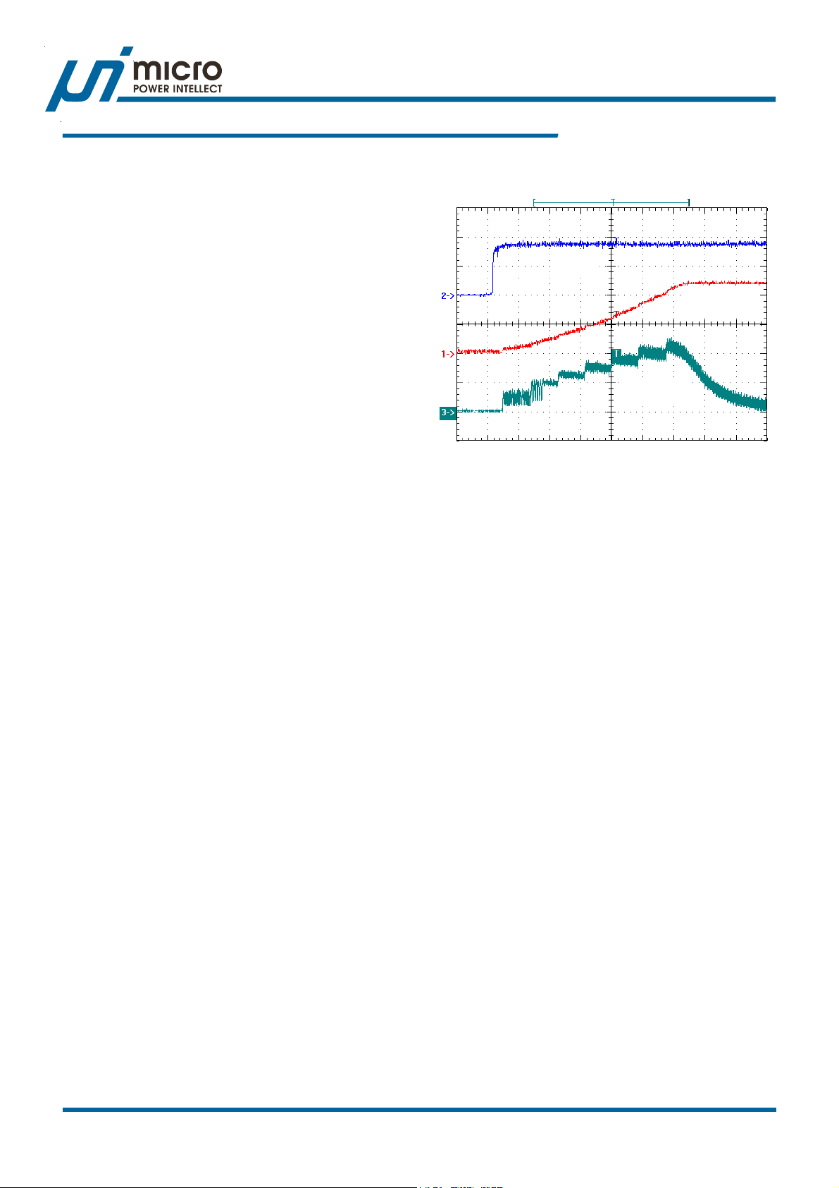
during the softstart cycle. Figure 1 illustrates the softstart
behavior of the uP6305. The inductor current ramps up
stairwisely with 250mA increments and 60us duration each
step. Note that the output capacitor is large to illustrate
the whole softstart behavior. The output voltage may ramp
up to its target level in 2 or 3 steps in real applications
where output capacitor is about 22uF.
EN
(2V/Div)
V
OUT
(0.5V/Div)
ILX
(500mA/Div)
Time (100us/Div)
Figure 1. Softstart of uP6305.
The uP6305 asserts end of soft start and set the current
limit to its normal level when the soft start duration expires.
After soft start end, the POK pin is set high impedance if
no fault occurs.
PWM Operation
The uP6305 adopts slope-compensated, current mode
PWM control capable of achieving 100% duty cycle. During
normal operation, the uP6305 operates at PWM mode to
regulate output voltage by transferring the power to the
output voltage cycle by cycle at a constant 1.0MHz
frequency. The uP6305 turns on the upper switch at each
rising edge of the internal oscillator allowing the inductor
current to ramp up linearly. The switch remains on until
either the current-limit is tripped or the PWM comparator
turns off the switch for regulating output voltage. The upper
switch current is sensed, slope compensated and
compared with the error amplifier output COMP to determine
the adequate duty cycle. The VOUT pin senses output
feedback voltage from an external resistive divider.
When the load current increases, it causes a slight
decrease in the feedback voltage relative to the 0.6V
reference, which in turn, causes the error amplifier output
voltage to increase until the average inductor current
matches the new load current.
Low Dropout Mode
The uP6305 increases duty cycle to maintain output voltage
within its regulation as the supply input drops gradually in
the battery-powered applications. The uP6305 operates with
100% duty cycle and enters low dropout mode as the supply
input approaches the output voltage. This maximizes the
battery life.
Rev. P00, File Name: uP6305-DS-P0002
4uPI Semiconductor Corp., http://www.upi-semi.com

Preliminary
uP6305
Functional Description
Output Voltage Setting and Feedback Network
The output voltage can be set from V
to VIN by a voltage
REF
divider as:
2R1R
V ×
The internal V
+
=
V
REFOUT
1R
is 0.6V with 1.5% accuracy. In real
REF
applications, a 22pF feedforward ceramic capacitor is
recommended in parallel with R2 for better transient
response.
Current Limit Function
The uP6305 continuously monitors the inductor current for
current limit by sensing the voltage drop across the upper
switch when it turns on. When the inductor current is higher
than current limit threshold (3.0A typical), the current limit
function activates and forces the upper switch turning off to
limit inductor current cycle by cycle. If the load continuously
demands more current than what uP6305 could provide,
uP6305 can not regulate the output voltage. Eventually
under voltage protection will be triggered and shuts down
the uP6305 if V
is too low.
OUT
Undervoltage Protection
Undervoltage Protection is triggered if the FB voltage is
lower than 0.15V and shuts down uP6305. The undervoltage
protection is latch-off type and can only be reset by POR
of VCC or toggling the EN pin.
Overvoltage Protection
Overvoltage protection (OVP) is triggered if the FB voltage
is higher than 0.8V and forces the uP6305 to continuous
PWM mode that allows the inductor current to be negative.
The voltage control loop will continuously turn on the lower
switch to sink charges from the output capacitor to lower
the output voltage. The lower switch turns off only the sinking
current is higher than it current limit level, typical 2.0A.
The uP6305 resumes normal operation if the OVP is
removed.
Over Temperature Protection (OTP)
The OTP is triggered and shuts down the uP6305 if the
junction temperature is higher than 150OC. The OTP is a
non-latch type protection. The uP6305 automatically
initiates another soft start cycle if the junction temperature
drops below 130OC.
Rev. P00, File Name: uP6305-DS-P0002
5uPI Semiconductor Corp., http://www.upi-semi.com
Preliminary
A
g
n
uP6305
bsolute Maximum Ratin
Supply Input Voltage, VIN, VCC(Note 1) --------------------------------------------------------------------------------------------- -0.3V to +6V
LX Pin Voltage
DC -------------------------------------------------------------------------------------------------------------------- -0.3V to +(VIN +0.3V)
<50ns -------------------------------------------------------------------------------------------------------------------- -5V to +(VIN +5V)
Other Pins --------------------------------------------------------------------------------------------------------------------------- -0.3V to (VCC + 0.3V
Storage Temperature Range ---------------------------------------------------------------------------------------------------- -65OC to +150OC
Junction Temperature ------------------------------------------------------------------------------------------------------------------------------------ 150OC
Lead Temperature (Soldering, 10 sec) ------------------------------------------------------------------------------------------------------------ 260OC
ESD Rating (Note 2)
HBM (Human Body Mode) --------------------------------------------------------------------------------------------------------------------- 2kV
MM (Machine Mode) ----------------------------------------------------------------------------------------------------------------------------- 200V
Thermal Informatio
Package Thermal Resistance (Note 3)
WQFN3x3-16L θJA ------------------------------------------------------------------------------------------------------------------------- 68°C/W
WQFN3x3-16L θJC ----------------------------------------------------------------------------------------------------------------------- 6°C/W
WLCSP1.5x1.5-9B θJA ----------------------------------------------------------------------------------------------------------------- 160°C/W
PSOP-8L θJA ------------------------------------------------------------------------------------------------------------------------- 50°C/W
PSOP-8L θJC ----------------------------------------------------------------------------------------------------------------------- 5°C/W
Power Dissipation, PD @ T
DFN3x3 -16 ----------------------------------------------------------------------------------------------------------------------------------------- 1.47W
WLCSP1.5x1.5-9B ------------------------------------------------------------------------------------------------------------------------------ 0.625W
PSOP-8L ----------------------------------------------------------------------------------------------------------------------------------------- 2.0W
= 25°C
A
Recommended Operation Conditions
Operating Junction Temperature Range (Note 4) ------------------------------------------------------------------------ -40OC to +125OC
Operating Ambient Temperature Range -------------------------------------------------------------------------------------- -40OC to +85OC
Supply Input Voltage, V
-------------------------------------------------------------------------------------------------------- +2.5V to +5.5V
IN
Electrical Characteristics
(VCC = VIN = 5V, TA = 25OC, unless otherwise specified)
retemaraPlobmySsnoitidnoCtseTniMpyTxaMstinU
tnerruCylppuS
egnaRegatloVylppuSV
tuokcoLegatloVrednUV
tnerruCtnecseiuQI
tnerruCnwodtuhSI
ecnerefeR
egatloVecnerefeRV
ycaruccAegatloVtuptuO ∆V
noitalugeReniLegatloVtuptuO ∆V
noitalugeRdaoLegatloVtuptuO ∆V
VNIV=
NI
V
OLVU
V
V
Q
V
NDHS
I
BF
I
TUO
V
TUO
I
TUO
CC
V,gnisiR
CC
CC
BF
V0=--10.01Au
NE
Am0=95.006.016.0V
TUO
Am0=5.1---5.1+%
TUO
NI
TUO
V=
NE
CC
V,gnillaF
V=
NE
CC
I,V8.0=
Am0=--4.3--Am
TUO
V5.5otV5.2=--40.04.0V/%
A2~A0=--5.0--A/%
5.2--5.5V
----5.2
V
2.2----
Rev. P00, File Name: uP6305-DS-P0002
6uPI Semiconductor Corp., http://www.upi-semi.com
 Loading...