

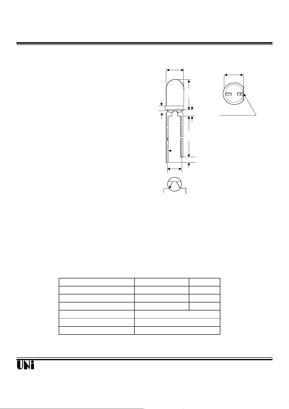
T-1 PACKAGE
NPN PHOTOTRANSISTOR
MID-30A22
Description
(.020)
(.040)
FLAT DENOTES COLLECTOR
E
The MID-30A22 is a NPN silicon phototransistor mounted in a lensed , special dark plastic package.The lens-
Package Dimensions
ψ3.00
(.118)
Unit: mm (inches )
4.00
(.157)
ing effect of the package allows an acceptance half view
angle of 10° that is measured from the optical axis to the
half power point .
1.00
0.50 TYP
Features
l Wide range of collector current
l Lensed for high sensitivity
l Low cost plastic package
l Good spectral matching to IRED (λp=940nm) type.
l Acceptance view angle : 20
o
Notes :
1. Tolerance is ± 0.25mm (.010") unless otherwise noted .
2. Protruded resin under flange is 1.5 mm (.059") max
3. Lead spacing is measured where the leads emerge from the package.
2.54
(.100)
5.25
(.207)
0.80±0.50
(.032±.020)
23.40MIN
(.920)
1.00MIN
(.040)
C
Absolute Maximum Ratings
Parameter Maximum Rating Unit
Power Dissipation 100 mW
Collector-Emitter Voltage 30 V
Emitter-Collector Voltage 5 V
Operating Temperature Range
Storage Temperature Range
Lead Soldering Temperature
Unity Opto Technology Co., Ltd.
@ TA=25oC
-55oC to +100oC
-55oC to +100oC
260℃ for 5 seconds
02/04/2002
MID-30A22
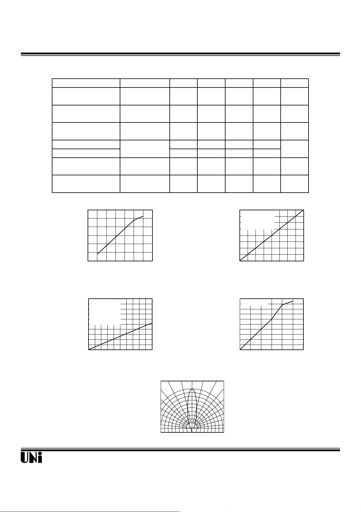
Optical-Electrical Characteristics
Ee=0.1mW/cm
CC
Ee=0.1mW/cm
VS IRRADIANCE
VS LOAD RESISTANCE
Tr Tf Rise and Fall Time -
0.5 0.3 0.1 0.2 0.4 0.6
70°
50°
VS AMBIENT TEMPERATURE
VS AMBIENT TEMPERATURE
Parameter Test Conditions Symbol Min. Typ . Max. Unit
Collector-Emitter
Breakdown Voltage Ee=0
Emitter-Collector Ie=0.1mA
Breakdown Voltage Ee=0
Collector-Emitter
Saturation Voltage
Rise Time
Fall Time
Collector Dark
Current Ee=0
On State Collector
Current
Ic=0.1mA V
Ic=0.5mA V
V
IC=1mA
VCE=10V I
VCE=5V I
2
=5V, RL=1KΩ
2
(BR)CEO
V
(BR)ECO
CE(SAT)
30 V
5 V
Tr 15
Tf 15
CEO
C(ON)
@ TA=25oC
0.4 V
µS
100 nA
2 mA
Typical Optical-Electrical Characteristic Curves
A
1000
µ
100
10
1
0.1
0.01
0.001
0 40 80 120
Iceo-Collector Dark Current -
S
µ
TA - Ambient Temperature -oC
FIG.1 COLLECTOR DARK CURRENT
200
Vcc = 5 V
VRL= 1 V
160
F = 100 Hz
120
PW = 1 ms
80
40
0
0 2 4 6 8 10
RL - Load Resistance - KΩ
FIG.3 RISE AND FALL TIME
FIG.2 NORMALIZED COLLECTOR CURRENT
0° 10° 20°
4.0
Vce =5 V
3.5
Ee =0.1 mW/cm
3.0
@λ= 940 nm
2.5
2.0
1.5
1.0
0.5
0.0
-75 -25 25 75 125
Normalized Collector Current
C
I
Relative Collector Current (mA)
TA - Ambient Temperature -oC
10
Vce = 5 V
8
6
4
2
0
0 0.1 0.2 0.3 0.4 0.5 0.6
Ee - Irradiance - mW/cm
2
2
FIG.4 RELATIVE COLLECTOR CURRENT
30°
Unity Opto Technology Co., Ltd.
1.0
0.9
0.8
Relative Sensitivity
FIG.5 SENSITIVITY DIAGRAM
40°
60°
80°
90°
02/04/2002
 Loading...