

18-Line SCSI Terminator (Reverse Disconnect)
UCC5617
FEATURES
Complies with SCSI, SCSI-2, SCSI-3,
•
SPI and FAST-20 Standards
2pF Channel Capacitance During
•
Disconnect
50mA Supply Current in Disconnect
•
Mode
110
•
•
•
•
• Trimmed Impedance to 5%
• Thermal Shutdown
• Current Limit
Termination
SCSI Hot Plugging Compliant, 10nA
Typical
+400mA Sinking Current for Active
Negation
–650mA Sourcing Current for
Termination
DESCRIPTION
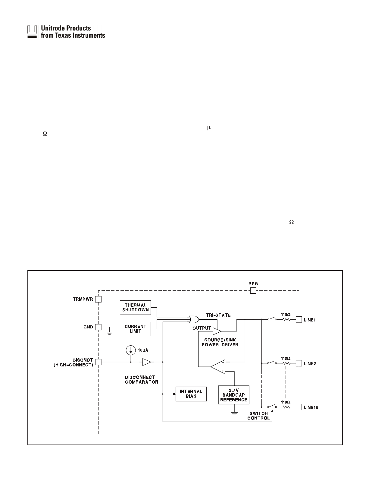
The UCC5617 provides 18 lines of active termination for a SCSI (Small
Computers Systems Interface) parallel bus. The SCSI standard recom
mends and Fast-20 (Ultra) requires active termination at both ends of the
cable.
Pin for pin compatible with the UC5609, the UCC5617 is ideal for high per
formance 5V SCSI systems, Termpwr 4.0-5.25V. During disconnect the
supply current is only 50
powered systems.
The UCC5617 is designed with a low channel capacitance of 2pF, which
eliminates effects on signal integrity from disconnected terminators at in
terim points on the bus.
The power amplifier output stage allows the UCC5617 to source full termi
nation current and sink active negation current when all termination lines
are actively negated.
The UCC5617, as with all Unitrode terminators, is completely hot pluggable
and appears as high impedance at the terminating channels with
TRMPWR = 0V or open.
Internal circuit trimming is utilized, first to trim the 110
then most importantly, to trim the output current as close to the maximum
SCSI-3 specification as possible, which maximizes noise margin in fast
SCSI operation.
A typical, which makes the IC attractive for lower
impedance, and
-
-
-
-
BLOCK DIAGRAM
This device is offered in low thermal resistance versions of the industry
standard 28 pin wide body SOIC.
Patented Circuit Design
SLUS351A - APRIL 1997 - REVISED AUGUST 2002
UDG-96073
UCC5617
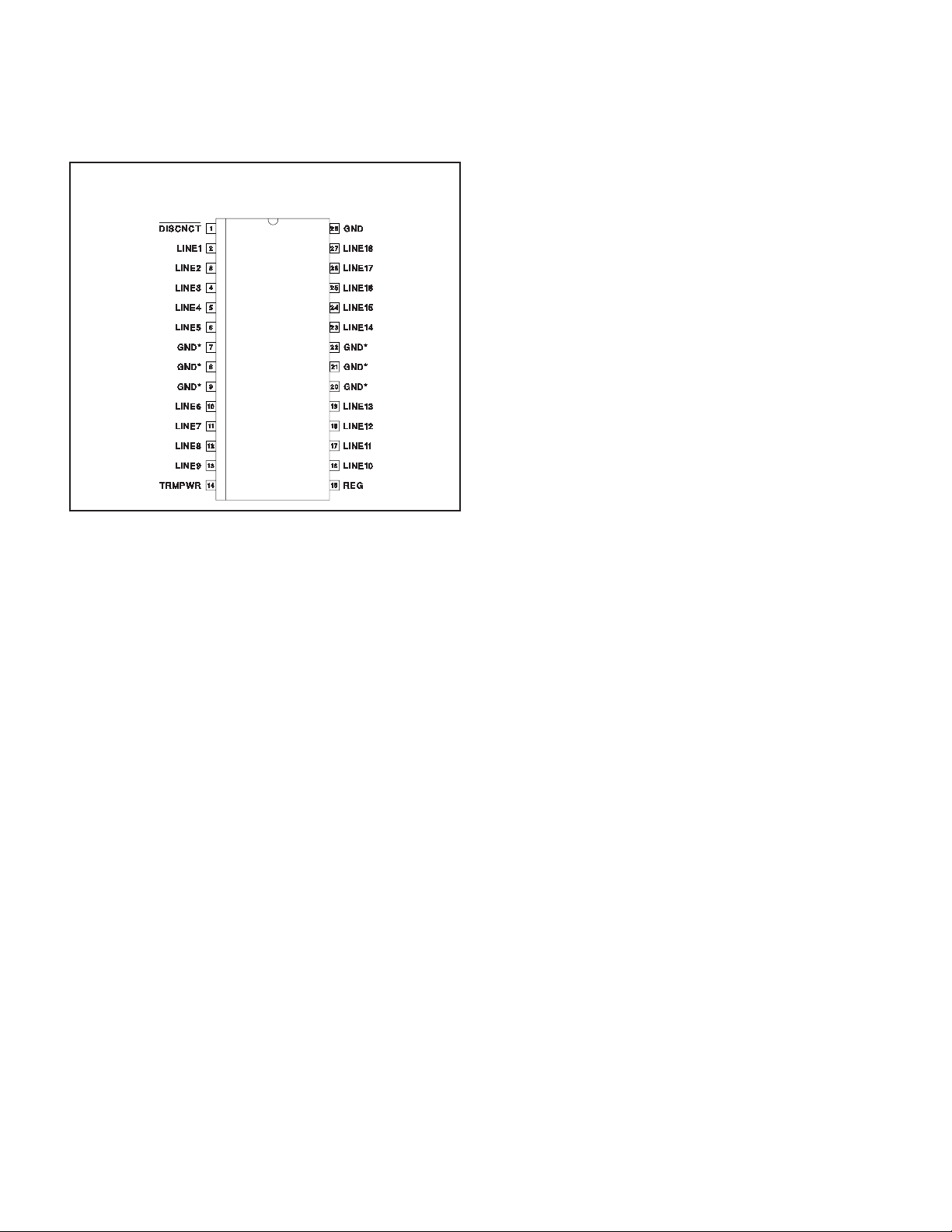
CONNECTION DIAGRAMS
SOIC-28 (Top View)
DWP Package
* DWP package pin 28 serves as signal ground; pins 7, 8, 9,
20, 21, 22 serve as heatsink/ground.
ABSOLUTE MAXIMUM RATINGS
TEMPWR. . . . . . . . . . . . . . . . . . . . . . . . . . . . . . . . . . . . . . . +7V
Signal Line Voltage . . . . . . . . . . . . . . . . . . . . . . . . . . 0V to +7V
Regulator Output Current . . . . . . . . . . . . . . . . . . . . . . . . . . . 1A
Storage Temperature . . . . . . . . . . . . . . . . . . . –65°C to +150°C
Operating Junction Temperature . . . . . . . . . . –55°C to +150°C
Lead Temperature (Soldering, 10 Seconds) . . . . . . . . . . 300°C
All currents are positive into, negative out of the specified
terminal. Consult Packaging Section of Databook for thermal
limitations and considerations of packages.
2

UCC5617
ELECTRICAL CHARACTERISTICS:
TRMPWR = 4.75V, DISCNCT = 0V, T
A=TJ
Unless otherwise stated these specifications apply for TA= 0°C to 70°C,
.
PARAMETER TEST CONDITIONS MIN TYP MAX UNITS
Supply Current Section
TERMPWR Supply Current All Termination Lines = Open 1 2 mA
All Termination Lines = 0.2V 420 440 mA
Power Down Mode DISCNCT
= 0V 50 100 A
Output Section (Termination Lines)
Termination Impedance (Note 3) 104.5 110 115.5
Output High Voltage V
Max Output Current V
TRMPWR
LINE
V
LINE
V
LINE
= 4V (Note 1) 2.6 2.8 3 V
= 0.2V, TJ= 25°C –22.1 –23.3 –24 mA
= 0.2V –20.7 –23.3 –24 mA
= 0.2V, TERMPWR = 4V, TJ= 25°C
–21 –23.3 –24 mA
(Note 1)
= 0.2V, TRMPWR = 4V (Note 1) –20 –23 –24 mA
V
LINE
= 0.5V –22.4 mA
V
LINE
Output Leakage DISCNCT
REG = 0.2V, V
Output Capacitance DISCNCT
= 2.4V, TRMPWR = 0V to 5.25V,
= 5.25V
LINE
= 2.4V (Note 2) 2 3.5 pF
10 400 nA
Regulator Section
Regulator Output Voltage 2.6 2.8 3 V
Drop Out Voltage All Termination Lines = 0.2V 0.4 0.8 V
Short Circuit Current V
Sinking Current Capability V
= 0V –475 –650 –850 mA
REG
= 3.5V 200 400 800 mA
REG
Thermal Shutdown 170 °C
Thermal Shutdown Hysteresis 10 °C
Disconnect Section
Disconnect Threshold 0.8 1.5 2 V
Input Current DISCNCT
= 0V –10 –30 A
Note 1: Measuring each termination line while other 17 are low (0.2V).
Note 2: Guaranteed by design. Not 100% tested in production.
Note 3: Tested by measuring I
OUT
with V
= 0.2V and V
OUT
with no load, then calculating:
OUT
VNL V
Z
=
..– ..02
OUT
IatV
OUT
02
PIN DESCRIPTIONS
DISCNCT: Taking this pin low causes the 18 channels to
become high impedance and the chip to go into
low-power mode; a high or open state allows the
channels to provide normal termination.
GND: Ground reference for the IC.
LINE1–LINE18: 110
termination channels.
REG: Output of the internal 2.8V regulator.
TRMPWR: Power for the IC.
3

APPLICATION INFORMATION
Procedure:
UCC5617
1) Measure V
2) Set V
= 0.2V
L
3) Measure I
4) Impedance =
N.L.
REG
at 0.2V
MAX
VNL V
REG
..–.02
I
MAX
Figure 1. Termline Impedance Measurement Circuit
UDG-96108
UDG-96074
4

PACKAGE OPTION ADDENDUM
www.ti.com
5-Feb-2007
PACKAGING INFORMATION
Orderable Device Status
(1)
Package
Type
Package
Drawing
Pins Package
Qty
Eco Plan
UCC5617DWP ACTIVE SOIC DW 28 20 Green (RoHS &
no Sb/Br)
UCC5617DWPG4 ACTIVE SOIC DW 28 20 Green (RoHS &
no Sb/Br)
UCC5617DWPTR ACTIVE SOIC DW 28 1000 Green (RoHS &
no Sb/Br)
UCC5617DWPTRG4 ACTIVE SOIC DW 28 1000 Green (RoHS &
no Sb/Br)
(1)
The marketing status values are defined as follows:
ACTIVE: Product device recommended for new designs.
LIFEBUY: TI has announced that the device will be discontinued, and a lifetime-buy period is in effect.
NRND: Not recommended for new designs. Device is in production to support existing customers, but TI does not recommend using this part in
a new design.
PREVIEW: Device has been announced but is not in production. Samples may or may not be available.
OBSOLETE: TI has discontinued the production of the device.
(2)
Eco Plan - The planned eco-friendly classification: Pb-Free (RoHS), Pb-Free (RoHS Exempt), or Green (RoHS & no Sb/Br) - please check
http://www.ti.com/productcontent for the latest availability information and additional product content details.
TBD: The Pb-Free/Green conversion plan has not been defined.
Pb-Free (RoHS): TI's terms "Lead-Free" or "Pb-Free" mean semiconductor products that are compatible with the current RoHS requirements
for all 6 substances, including the requirement that lead not exceed 0.1% by weight in homogeneous materials. Where designed to be soldered
at high temperatures, TI Pb-Free products are suitable for use in specified lead-free processes.
Pb-Free (RoHS Exempt): This component has a RoHS exemption for either 1) lead-based flip-chip solder bumps used between the die and
package, or 2) lead-based die adhesive used between the die and leadframe. The component is otherwise considered Pb-Free (RoHS
compatible) as defined above.
Green (RoHS & no Sb/Br): TI defines "Green" to mean Pb-Free (RoHS compatible), and free of Bromine (Br) and Antimony (Sb) based flame
retardants (Br or Sb do not exceed 0.1% by weight in homogeneous material)
(2)
Lead/Ball Finish MSL Peak Temp
CU NIPDAU Level-2-260C-1 YEAR
CU NIPDAU Level-2-260C-1 YEAR
CU NIPDAU Level-2-260C-1 YEAR
CU NIPDAU Level-2-260C-1 YEAR
(3)
(3)
MSL, Peak Temp. -- The Moisture Sensitivity Level rating according to the JEDEC industry standard classifications, and peak solder
temperature.
Important Information and Disclaimer:The information provided on this page represents TI's knowledge and belief as of the date that it is
provided. TI bases its knowledge and belief on information provided by third parties, and makes no representation or warranty as to the
accuracy of such information. Efforts are underway to better integrate information from third parties. TI has taken and continues to take
reasonable steps to provide representative and accurate information but may not have conducted destructive testing or chemical analysis on
incoming materials and chemicals. TI and TI suppliers consider certain information to be proprietary, and thus CAS numbers and other limited
information may not be available for release.
In no event shall TI's liability arising out of such information exceed the total purchase price of the TI part(s) at issue in this document sold by TI
to Customer on an annual basis.
Addendum-Page 1
 Loading...