

UNITRODE UCC1946, UCC2946, UCC3946 Technical data
查询UCC1946供应商
Microprocessor Supervisor with Watchdog Timer
UCC1946
UCC2946
UCC3946
FEATURES
Fully Programmable Reset Threshold
•
Fully Programmable Reset Period
•
Fully Programmable Watchdog Period
•
2% Accurate Reset Threshold
•
VDD Can Go as Low as 2V
•
18µA Maximum IDD
•
Reset Valid Down to 1V
•
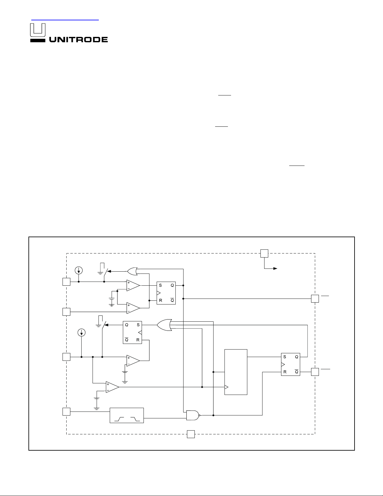
BLOCK DIAGRAM
400nA
DESCRIPTION
The UCC3946 is designed to provide accurate microprocessor supervi
sion, including reset and watchdog functions. During power up, the IC
asserts a reset signal RES
mains asserted until the VDD voltage rises and remains above the re
set threshold for the reset period. Both reset threshold and reset period
are programmable by the user. The IC is also resistant to glitches on
the VDD line. Once RES
threshold voltage need to be of certain time duration and voltage mag
nitude to generate a reset signal. These values are shown in Figure 1.
An I/O line of the microprocessor may be tied to the watchdog input
(WDI) for watchdog functions. If the I/O line is not toggled within a set
watchdog period, programmable by the user, WDO
The watchdog function will be disabled during reset conditions.
The UCC3946 is available in 8-pin SOIC(D), 8-pin DIP (N or J) and
8-pin TSSOP(PW) packages to optimize board space.
with VDD as low as 1V. The reset signal re
has been deasserted, any drops below the
will be asserted.
VDD
8
POWER TO
CIRCUITRY
-
-
-
-
4RP
1.235V .
WP
2RTH
400nA
6
1.235V
7WDI
POWER ON RESET
100mV
WATCHDOG TIMING
EDGE DETECT
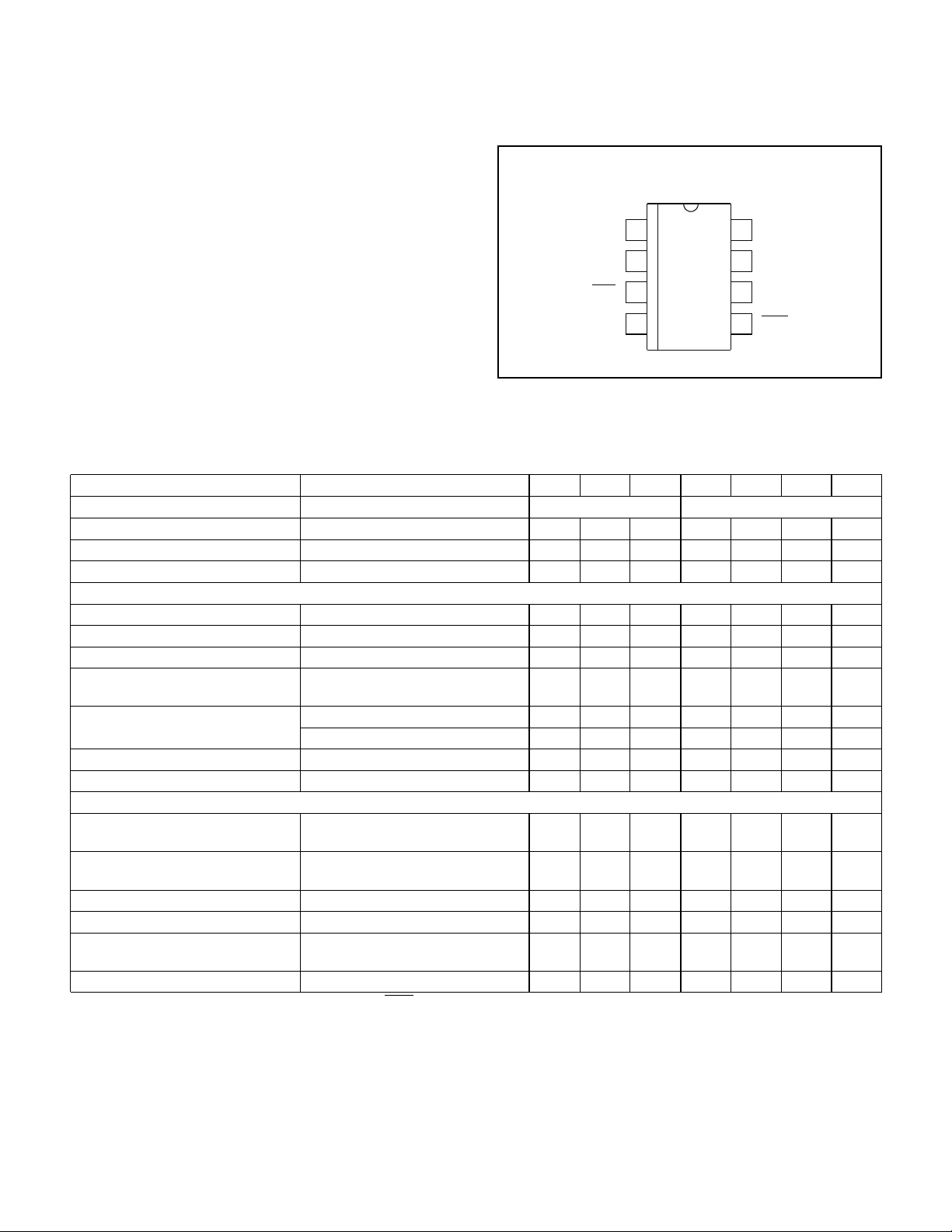
Note: Pinout represents the 8-pin TSSOP package.
1
GND
8-BIT COUNTER
A3
A2
CLR
A1
A0
CLK
3RES
5
WDO
UDG-98001
SLUS247B - FEBRUARY 2000
UCC1946
UCC2946
UCC3946
ABSOLUTE MAXIMUM RATINGS
VIN . . . . . . . . . . . . . . . . . . . . . . . . . . . . . . . . . . . . . . . . . . . . 10V
Storage Temperature . . . . . . . . . . . . . . . . . . . –65°C to +150°C
Junction Temperature. . . . . . . . . . . . . . . . . . . –55°C to +150°C
CONNECTION DIAGRAM
SOIC-8, TSSOP-8, DIL-8 (Top View)
D, PW, N or J Package
Lead Temperature (Soldering, 10 sec.). . . . . . . . . . . . . +300°C
Currents are positive into, negative out of the specified terminal.
Consult Packaging Section of the Databook for thermal limita
tions and considerations of packages.
ELECTRICAL CHARACTERISTICS:
Unless otherwise specified, VDD = 2.1V to 5.5V for UCC1946 and UCC2946;
GND
1
-
2
RTH
RES
3
4
RP
8
VDD
7
WDI
6
WP
5
WDO
VDD = 2V to 5.5V for UCC3946; TA = 0°C to 70°C for UCC3946, –40°C to 95°C for UCC2946, and –55°C to 125°C for UCC1946;
T
A =TJ
PARAMETERS TEST CONDITIONS MIN TYP MAX MIN TYP MAX UNITS
UCC3946 UCC1946 & UCC2946
Operating Voltage 2.0 5.5 2.1 5.5 V
Supply Current 10 18 12 18 µA
Minimum VDD (Note 1) 1 1.1 V
Reset Section
Reset Threshold VDD Rising 1.210 1.235 1.260 1.170 1.235 1.260 V
Threshold Hysteresis 15 15 mV
Input Leakage 55nA
Output High Voltage I
Output Low Voltage I
SOURCE = 2mA VDD –
0.3
SINK = 2mA 0.1 0.1 V
VDD = 1V, I
SINK = 20uA 0.2 0.4 V
VDD –
0.3
V
VDD to Output Delay VDD = -1mV/µs (Note 2) 120 120 µs
Reset Period C
RP = 64nF 160 200 260 140 200 320 ms
Watchdog Section
WDI Input High 0.7·
V
DD
WDI Input Low 0.3·
VDD
Watchdog Period C
WP = 64nF 1.12 1.60 2.08 0.96 1.60 2.56 s
0.7·
V
DD
0.3·
V
DD
V
V
Watchdog Pulse Width 50 50 ns
Output High Voltage I
Output Low Voltage I
SOURCE = 2mA VDD –
0.3
SINK = 2mA 0.1 0.1 V
VDD –
0.3
V
Note 1: This is the minimum supply voltage where RES is considered valid.
Note 2: Guaranteed by design.Not 100% tested in production.
2
 Loading...