

查询UCC19411供应商
Low Power Synchronous Boost Converter
FEATURES
1V Input Voltage Operation Start-up
•
Guaranteed under FULL Load on
Main Output, and Operation Down to
0.5V
200mW Output Power at Battery
•
Voltages as low as 0.8V
Secondary 7V Supply from a Single
•
Inductor
Output Fully Disconnected in
•
Shutdown
Adaptive Current Mode Control for
•
Optimum Efficiency
High Efficiency over Wide Operating
•
Range
• 6µA Shutdown Supply Current
• Output Reset Function with
Programmable Reset Period
DESCRIPTION
The UCC39411 family of low input voltage, single inductor boost
converters is optimized to operate from a single or dual alkaline cell, and
steps up to a 3.3V, 5V, or adjustable output at 200mW. The UCC39411
family also provides an auxiliary 7V output, primarily for the gate drive
supply, which can be used for applications requiring an auxiliary output,
such as 5V, by linear regulating. The primary output will start up under full
load at input voltages typically as low as 0.8V with a guaranteed max of
1V, and will operate down to 0.5V once the converter is operating,
maximizing battery utilization.
The UCC39411 family is designed to accommodate demanding
applications such as pagers and cell phones that require high efficiency
over a wide operating range of several milli-watts to a couple of hundred
milli-watts. High efficiency at low output current is achieved by optimizing
switching and conduction losses with a low total quiescent current (50µA).
At higher output current the 0.5Ω switch, and 1.2Ω synchronous rectifier
along with continuous mode conduction provide high power efficiency. The
wide input voltage range of the UCC39411 family can accommodate other
power sources such as NiCd and NimH.
The 39411 family also provides shutdown control. Packages available are
the 8 pin SOIC (D), 8 pin DIP (N or J), and 8 pin TSSOP (PW) to optimize
board space.
application
INFO
available
UCC19411/2/3
UCC29411/2/3
UCC39411/2/3
PRELIMINARY
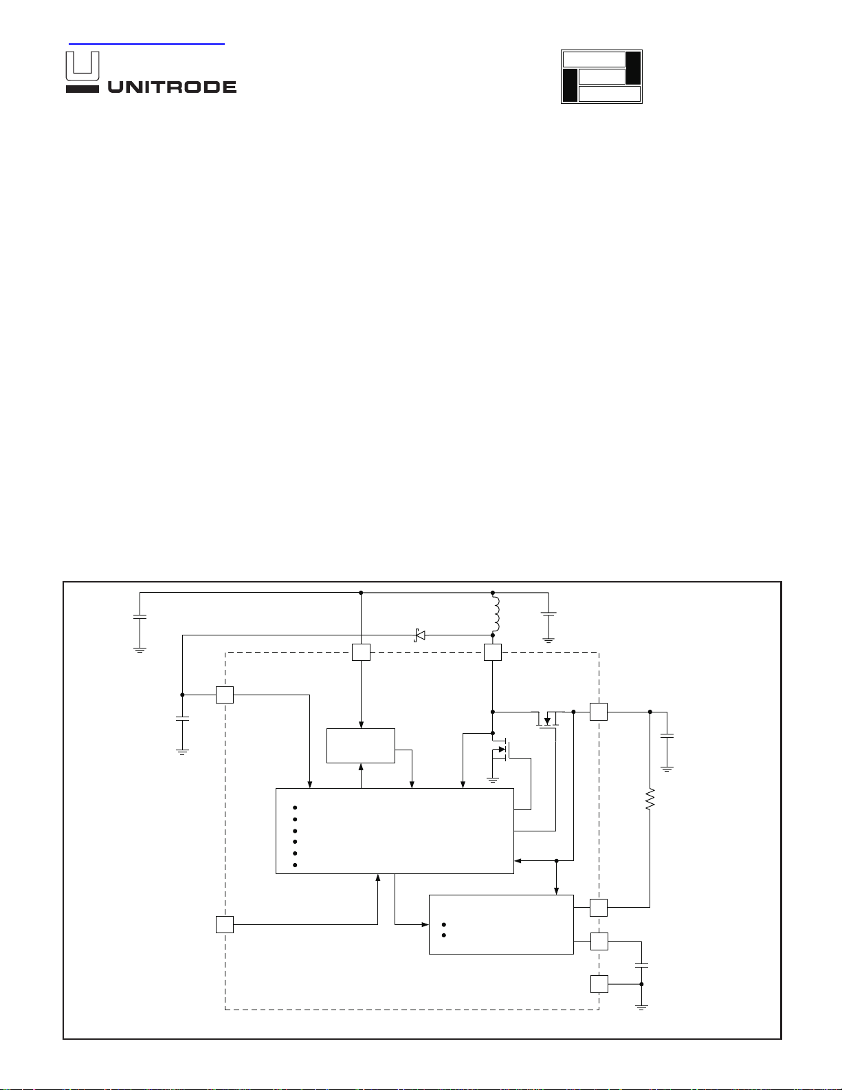
SIMPIFIED BLOCK DIAGRAM AND APPLICATION CIRCUIT (UCC39412)
100µF
VGD
100µF
22µH
1
VIN
8
START-UP
CIRCUITRY
MODULATOR CONTROL CIRCUIT
SYNCHRONOUS RECTIFICATION CIRCUITRY
ANTI-CROSS CONDUCTION
START-UP
MULTIPLEXING LOGIC
MAX INPUT POWER CONTROL
ADAPTIVE CURRENT CONTROL
RESET CONTROL CIRCUIT
2SD/FB
GLITCH SUPRESSION
PROGRAMMABLE TIMING
SW
6
+
1.2Ω
0.5Ω
1V TO 3.5V
VOUT
7
3
4
5
3.3V 200mW
RESB
CT
C
GND
100µF
R
RES
T
Note: Pinout shown is for the TSSOP Package. Consult Package Descriptions for DIP and SOIC configurations.
SLUS245A - MARCH 1999
UDG-98067
ABSOLUTE MAXIMUM RATINGS
VIN Voltage . . . . . . . . . . . . . . . . . . . . . . . . . . . . . . –0.3V to 10V
SD Voltage . . . . . . . . . . . . . . . . . . . . . . . . . . . . . . . –0.3V to V
VGD Voltage . . . . . . . . . . . . . . . . . . . . . . . . . . . . –0.3V to 14V
SW Voltage . . . . . . . . . . . . . . . . . . . . . . . . . . . . . . –0.3V to 15V
Currents are positive into, negative out of the specific terminal.
Consult Packaging Section of the Databook for thermal limita
tions and considerations of packages.
IN
-
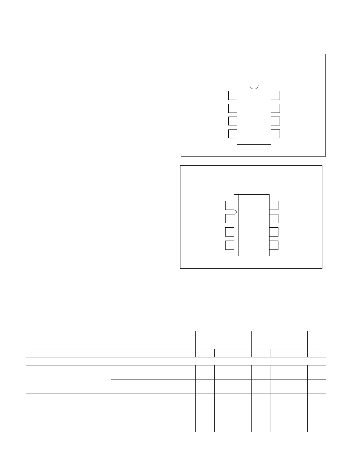
CONNECTION DIAGRAMS
DIL-8, SOIC-8 (TOP VIEW)
N or J Package, D Package
VOUT
VGD
1
2
UCC19411/2/3
UCC29411/2/3
UCC39411/2/3
8
SW
7
GND
VIN
3
SD/FB
4
TSSOP-8 (TOP VIEW)
PW Package
VIN
1
CT
2
3
4
SD/FB
RESB
6
CT
5
RESB
8
VGD
7
VOUT
6
SW
5
GND
ELECTRICAL CHARACTERISTICS:
UCC29411/2/3, T
= –55C to +125°C for the UCC19411/2/3, VIN= 1.25V for UCC39411/2, VIN= 2.5V for the UCC39413, TA=TJ.
J
TJ= 0°C to +70°C for the UCC39411/2/3, TJ= –40°C to +85°C for the
UCC39411
UCC39412
UCC39413
UCC19411/2/3
UCC29411/2/3
PARAMETER TEST CONDITIONS MIN TYP MAX MIN TYP MAX UNITS
VIN Section
Minimum Start-up Voltage No External VGD Load, T
I
=60mA (Note 1)
OUT
No External VGD Load, I
=25°C,
J
OUT
=60mA
0.8 1 .08 1 V
0.9 1.1 1.2 1.4 V
(Note 1)
Minimum Dropout Voltage No External VGD Load, I
OUT
=10mA
0.5 0.7 V
(Note 1)
Input Voltage Range 1.1 3.2 1.3 3.2 V
Quiescent Supply Current (Note 2) 6 12 8 16
Supply Current at Shutdown SD = GND 6 12 8 16
2
µA
µA
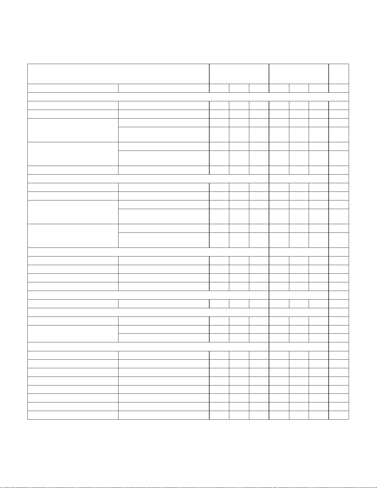
UCC19411/2/3
UCC29411/2/3
UCC39411/2/3
ELECTRICAL CHARACTERISTICS:
UCC29411/2/3, T
= –55C to +125°C for the UCC19411/2/3, VIN= 1.25V for UCC39411/2, VIN= 2.5V for the UCC39413, TA=TJ.
J
TJ= 0°C to +70°C for the UCC39411/2/3, TJ= –40°C to +85°C for the
UCC39411
UCC39412
UCC39413
UCC19411/2/3
UCC29411/2/3
PARAMETER TEST CONDITIONS MIN TYP MAX MIN TYP MAX UNITS
Output Section
Quiescent Supply Current (Note 2) 15 28 20 37
Supply Current at Shutdown SD = GND 3 6 5 10
Regulation Voltage (UCC39412) 1V < V
1V < V
< 3V 3.2 3.3 3.39 3.15 3.3 3.45 V
IN
< 3V, 0mA<I
IN
OUT
<60mA
3.17 3.3 3.43 3.11 3.3 3.5 V
(Note 1)
Regulation Voltage (UCC39413) 1V < V
1V < V
< 5V 4.85 5 5.15 4.78 5 5.23 V
IN
< 5V, 0mA<I
IN
OUT
<60mA
4.8 5 5.2 4.71 5 5.3 V
(Note 1)
ADJ Voltage (UCC39411) 1V < V
< 3V 1.212 1.25 1.288 1.194 1.25 1.306 V
IN
VGD Output Section
Quiescent Supply Current (Note 2) 20 40 27 55
Supply Current at Shutdown SD = GND 20 40 27 55
Regulation Voltage
(UCC39411/2)
1V < V
1V < V
< 3V 6.3 7 7.7 6.3 7 7.7 V
IN
< 3V, 0mA<I
IN
OUT
<10mA
6.3 7 7.7 6.3 7 7.7 V
(Note 1)
Regulation Voltage (UCC39413) 1V < V
1V < V
< 5V 7.7 8.5 9.3 7.7 8.5 9.3 V
IN
< 5V, 0mA<I
IN
OUT
<10mA
7.7 8.5 9.3 7.7 8.5 9.3 V
(Note 1)
Inductor Charging Section (L=22
µH)
Peak Discontinuous Current Operating Range, L=22.1µH 180 250 300 180 250 300 mA
Peak Continuous Current 385 550 715 385 550 715 mA
Charge Switch RDS
ON
D Package 0.5 0.75 0.6 0.85 Ω
Current Limit Delay (Note 1) 50 50 ns
Synchronous Rectifier Section
Rectifier RDS
ON
D Package 1.2 1.8 1.4 2.16 Ω
Shutdown Section
Threshold 0.4 0.6 0.8 0.2 0.6 0.9 V
Input Bias Current SD = GND 2 5 15 2 5 15
SD = 1.25V 5 20 20 100 nA
Reset Section
Threshold (UCC39411) 1.08 1.125 1.17 1.07 1.125 1.18 V
Threshold (UCC39412) 2.85 2.97 3.09 2.83 2.97 3.11 V
Threshold (UCC39413) 4.32 4.5 4.68 4.3 4.5 4.7 V
Reset Period C
to Reset Delay V
V
OUT
= 0.15µF 113 188 263 94 188 282 ms
T
Falling at –1mV/µs (Note 1) 60 60 µs
OUT
Sink Current 1 20 1 20 mA
Output Low Voltage I
= 500µA 0.1 0.1 V
OUT
Output Leakage 0.5 0.5
Note 1 : Guaranteed by design and alternate test methods. Not 100% tested in production.
Note 2: For the UCC39411 FB=1.306V, VGD=7.7V, For the UCC39412 V
V
=5.3V, VGD=9.3V.
OUT
=3.5V and VGD=7.7V, For the UCC39413
OUT
µA
µA
µA
µA
µA
µA
3
 Loading...