

UNITRODE UCC1857, UCC2857, UCC3857 Technical data
查询UCC1857供应商
Isolated Boost PFC Preregulator Controller
UCC1857
UCC2857
UCC3857
PRELIMINARY
FEATURES
• PFC With Isolation, V
• Single Power Stage
• Zero Current Switched IGBT
• Programmable ZCS Time
• Corrects PF to >0.99
• Fixed Frequency, Average Current
Control
• Improved RMS Feedforward
• Soft Start
• 9V to 18V Supply V Range
• 20-Pin DW, N, J, and L Packages
< V
O
IN
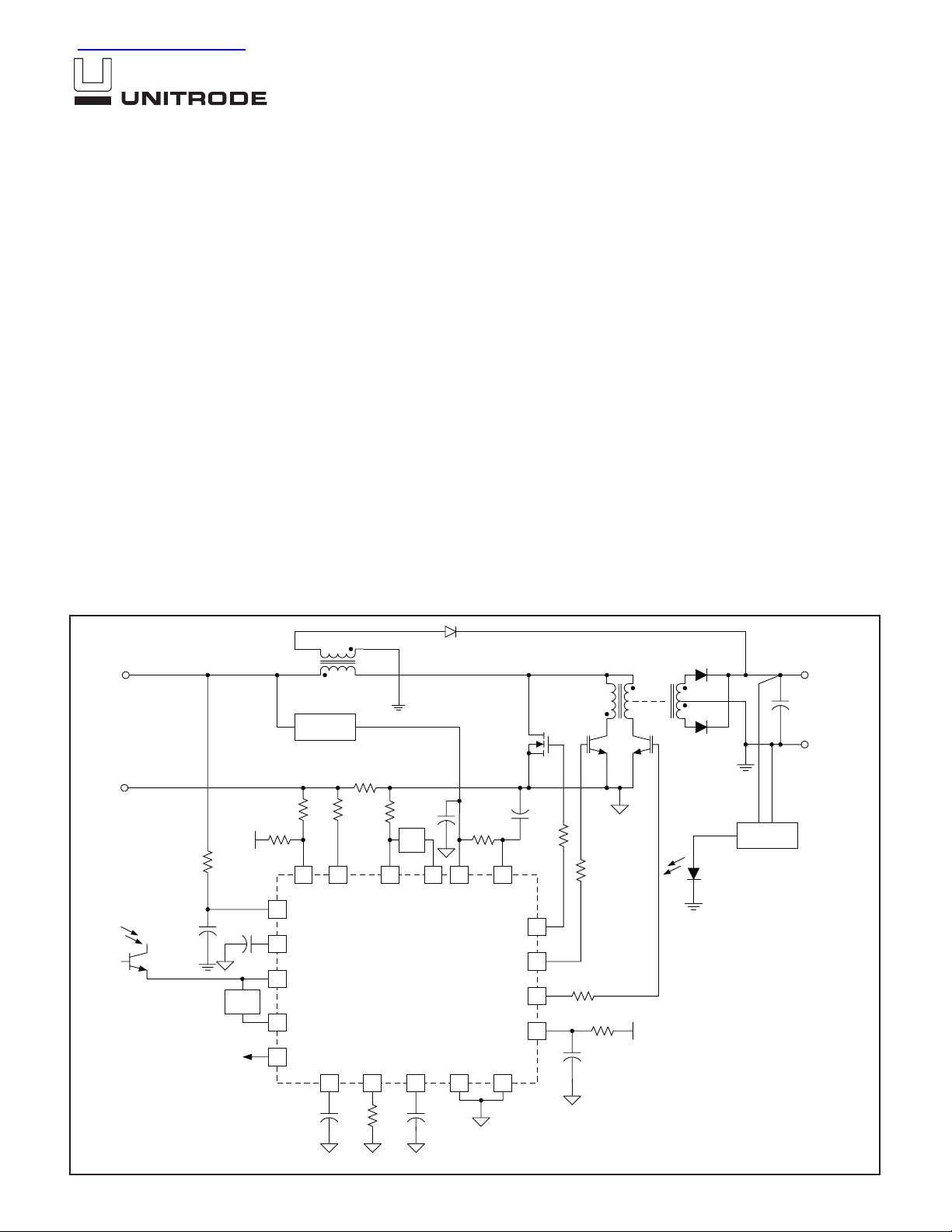
TYPICAL APPLICATION CIRCUIT
DESCRIPTION
The UCC3857 provides all of the control functions necessary for an Isolated Boost PFC Converter. These converters have the advantage of transformer isolation between primary and secondary, as well as an output bus
voltage that is lower than the input voltage. By providing both power factor
correction and down conversion in a single power processing stage, the
UCC3857 is ideal for applications which require high efficiency, integration,
and performance.
The UCC3857 brings together the control functions and drivers necessary
to generate overlapping drive signals for external IGBT switches, and provides a separate output to drive an external power MOSFET which provides zero current switching (ZCS) for both the IGBTs. Full programmability
is provided for the MOSFET driver delay time with an external RC network.
ZCS for the IGBT switches alleviates the undesirable turn off losses typically associated with these devices. This allows for higher switching frequencies, smaller magnetic components and higher efficiency. The power
factor correction (PFC) portion of the UCC3857 employs the familiar average current control scheme used in previous Unitrode controllers. Internal
circuitry changes, however, have simplified the design of the PFC section
and improved performance.
(continued)
RECTIFIED
AC INPUT
R
REF
CKT
+
C
F
V
OUT
–
T1
BIAS
SUPPLY
R
S
REF
AC
Z
V
13 73
1IAC
2
CRMS
10 VA–
11 VAO
5VREF
SS
20
UCC3857
RT
19
Z
C
8 154
VINCAOCA–MOUTPKLMT
PGND
CT
20
AGND
17
QA
VD
14MOSDRV
16IGDRV1
18IGDRV2
12DELAY
6
Q2Q1
FEEDBACK
OPTO
REF
02/99
UDG-98065
ABSOLUTE MAXIMUM RATINGS
Input Supply Voltage (VIN, VD). . . . . . . . . . . . . . . . . . . . . . 18V
General Analog/Logic Inputs
(CRMS, MOUT, CA–, VA–, CT, RT, PKLMT)
(Maximum Forced Voltage). . . . . . . . . . . . . . . . –0.3V to 5V
IAC (Maximum Forced Current) . . . . . . . . . . . . . . . . . . . 300µA
Reference Output Current . . . . . . . . . . . . . . . Internally Limited
Output Current (MOSDRV, IGDRV1, IGDRV2)
Pulsed. . . . . . . . . . . . . . . . . . . . . . . . . . . . . . . . . . . . . . . . 1A
Continuous . . . . . . . . . . . . . . . . . . . . . . . . . . . . . . . . 200mA
Storage Temperature . . . . . . . . . . . . . . . . . . . −65°C to +150°C
Junction Temperature. . . . . . . . . . . . . . . . . . . −55°C to +150°C
Lead Temperature (Soldering, 10 Sec.). . . . . . . . . . . . . +300°C
Unless otherwise indicated, voltages are reference to ground
and currents are positive into, negative out of the specified terminal. Pulsed is defined as a less than 10% duty cycle with a
maximum duration of 500 s. Consult Packaging Section of
Databook for thermal limitations and considerations of packages.
UCC1857
UCC2857
UCC3857
DESCRIPTION (continued)
Controller improvements include an internal 6 bit A-D
converter for RMS input line voltage detection, a zero
load power circuit, and significantly lower quiescent operating current. The A-D converter eliminates an external
2 pole low pass filter for RMS detection.
This simplifies the converter design, eliminates 2nd harmonic ripple from the feedforward component, and provides an approximate 6 times improvement in input line
transient response. The zero load power comparator
prevents energy transfer during open load conditions
without compromising power factor at light loads. Low
startup and operating currents which are achieved
through the use of Unitrode's BCDMOS process simplify
the auxiliary bootstrap supply design.
Additional features include: under voltage lockout for reliable off-line startup, a programmable over current shutdown, an auxiliary shutdown port, a precision 7.5V
reference, a high amplitude oscillator ramp for improved
noise immunity, softstart, and a low offset analog square,
multiple and divide circuit. Like previous Unitrode PFC
controllers, worldwide operation without range switches
is easily implemented.
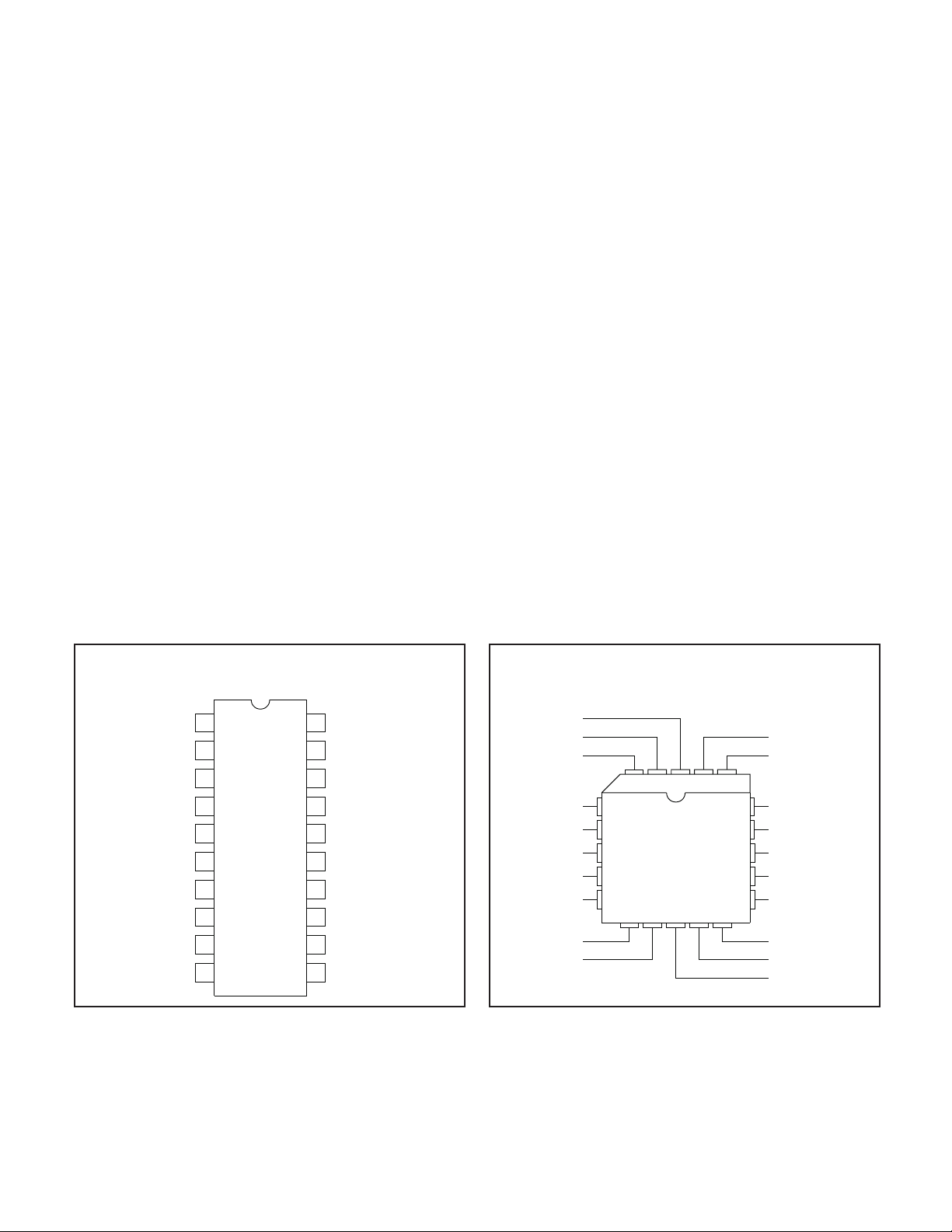
CONNECTION DIAGRAMS
DIL-20, SOIC- 20 (Top View)
J, N and DW Packages
IAC
1
2
CRMS
MOUT
3
4
VIN
5
VREF
6
AGND
7
CA–
CAO
8
9
SS DELAY
10VA–
20
19
18
17
16
15
14
13
12
11
CT
RT
IGDRV2
PGND
IGDRV1
VD
MOSDRV
PKLMT
VAO
PLCC-20 (Top View)
L Package
IAC
CRMS
MOUT
3
VIN
VREF
AGND
CA–
CAO
VA–
4
5
6
7
8
91110 12 13
SS
122019
18
17
16
15
14
CT
RT
IGDRV2
PGND
IGDRV1
VD
MOSDRV
PKLMT
DELAY
VAO
2

UCC1857
UCC2857
UCC3857
ELECTRICAL CHARACTERISTICS:
UCC3857, –40°C to +85°C for the UCC2857, and –55°C to +125°C for the UCC1857, V
Unless otherwise stated, these specifications apply for TA= 0°C to 70°C for the
, VVD= 12V, RT= 19.2K, CT= 680pF.
VIN
TA= TJ.
PARAMETER TEST CONDITIONS MIN TYP MAX UNITS
Input Supply
Supply Current, Active No Load on Outputs, V
Supply Current, Startup No Load on Outputs, V
VD
VD
= V
= V
VIN
VIN
3.5 5 mA
60 TBD µA
VIN UVLO Threshold 13.75 15.5 V
UVLO Threshold Hysteresis 3 3.75 TBD V
Reference
Output Voltage (V
)T
VREF
= 25°C, I
J
= 1mA 7.387 7.5 7.613 V
REF
Over Temperature, UCC3857 7.368 7.5 7.631 V
Over Temperature, UCC1857, UCC2857 7.313 7.5 7.687 V
Load Regulation I
Line Regulation V
Short Circuit Current V
= 1mA to 10mA 2 10 mV
REF
= VVD= 12V to 16V 2 15 mV
VIN
= 0V –55 –30 mA
VREF
Current Amplifier
Input Offset Voltage (Note 1) –3 0 3 mV
Input Bias Current (Note 1) –50 nA
Input Offset Current (Note 1) 25 nA
CMRR V
AVOL VCM= 0V, V
= 0V to 1.5V, V
CM
= 2V to 5V 65 85 dB
CAO
VOH Load on CAO = 50µA, V
VOL Load on CAO = 50µA, V
Maximum Output Current Source : V
Sink : V
CA–
= 0V, V
CA–
= 1V, V
= 3V 80 dB
CAO
MOUT
MOUT
= 1V, V
MOUT
= 0V, VCA– = 1V 0.2 V
MOUT
= 1V, V
= 0V, V
CAO
= 0V 6 7 V
CA–
= 3V –150 µA
CAO
= 3V 5 30 50 mA
Gain Bandwidth Product fIN= 100kHz, 10mV p – p 3 5 MHz
Voltage Amplifier
,
V
Input Voltage Measured on V
Input Bias Current Measured on V
AVOL V
VOH Load on V
VOL Load on V
Maximum Output Current Source: V
= 1V to 5V 75 dB
VAO
VAO
VAO
VA–
Sink: V
VA–
= 3.2V, V
VA–
VA–
= –50µA, V
= 50µA, V
= 2.8V, V
= 3V 2.9 3 3.1 V
VAO
,
V
= 3V –50 nA
VAO
= 2.8V 5.3 5.55 5.7 V
VA–
= 3.2V 0.1 0.45 V
VA–
= 3V –20 –12 –5 mA
VAO
= 3V 5 20 30 mA
VAO
Oscillator
Initial Accuracy T
= 25°C 42.5 50 57.5 kHz
J
40 50 60 kHz
Voltage Stability V
= 12V to 18V 1 %
VIN
CT Ramp Peak-Valley Amplitude 4 4.5 5 V
CT Ramp Valley Voltage 1.5 V
Output Drivers
VOH IL = –100mA 9 10 V
VOL IL = 100mA 0.1 0.5 V
Rise Time C
Fall Time C
= 1nF 25 TBD ns
LOAD
= 1nF 10 TBD ns
LOAD
Trailing Edge Delay
Delay Time R
= 12k, CD= 200pF, V
D
= 4V 1.6 2 2.4 µs
VAO
3
 Loading...