

查询UCC1839供应商
Secondary Side Average Current Mode Controller
UCC1839
UCC2839
UCC3839
FEATURES
• Practical Secondary Side Control of
Isolated Power Supplies
• Provides a Self Regulating Bias
Supply From a High Input Voltage
Using an External N-Channel
Depletion Mode FET
• Onboard Precision, Fixed Gain,
Differential Current Sense Amplifier
• Wide Bandwidth Current Error
Amplifier
• 5V Reference
• High Current, Programmable Gm
Amplifier Optimized to Drive
Opto-couplers
DESCRIPTION
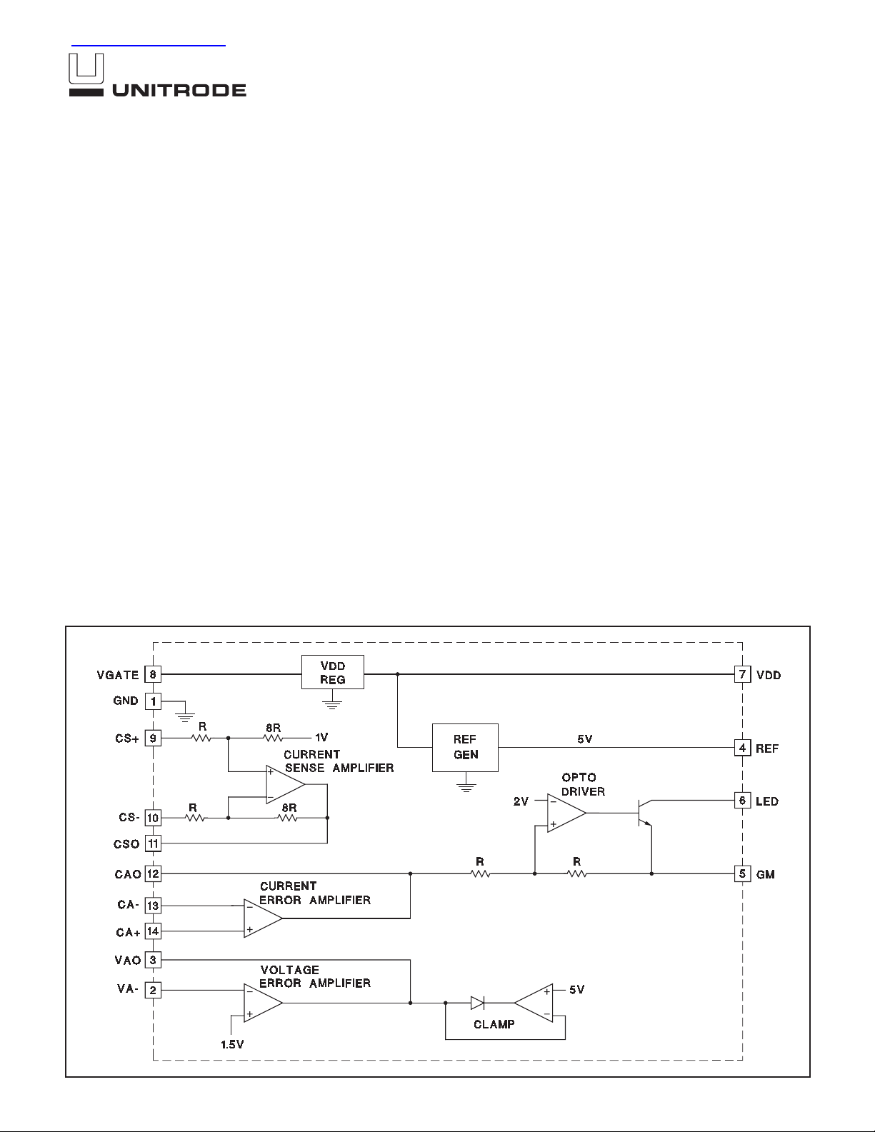
The UCC3839 provides the control functions for secondary side average
current mode control in isolated power supplies. Start up, pulse width
modulation and MOSFET drive must be accomplished independently on
the primary side. Communication from secondary to primary side is anticipated through an opto-isolator.
Accordingly, the UCC3839 contains a fixed gain current sense amplifier,
voltage and current error amplifiers, and a Gm type buffer/driver amplifier
for the opto-isolator. Additional housekeeping functions include a precision
5V reference and a bias supply regulator.
Power for the UCC3839 can be generated by peak rectifying the voltage of
the secondary winding of the isolation transformer. From this unregulated
voltage, the UCC3839’s bias supply regulator will generate its own 7.5V
bias supply using an external, N-channel, depletion mode FET.
The UCC3839 can be configured for traditional average current mode control where the output of the voltage error amplifier commands the current
error amplifier. It can also be configured for output voltage regulation with
average current mode short circuit current limiting, employing two parallel
control loops regulating the output voltage and output current independently.
BLOCK DIAGRAM
04/99
UDG-97011
ABSOLUTE MAXIMUM RATINGS
Supply Voltage . . . . . . . . . . . . . . . . . . . . . . . . . . . . . . . . . . 15V
Supply Current
(LED not connected) . . . . . . . . . . . . . . . . . . . . . . . . . . . 2mA
(LED connected) . . . . . . . . . . . . . . . . . . . . . . . . . . . . . 14mA
Analog Inputs . . . . . . . . . . . . . . . . . . . . . . . . . . . . –0.3V to 15V
Power Dissipation at TA = 60°C
(LED not connected). . . . . . . . . . . . . . . . . . . . . . . . . . 20mW
(LED connected). . . . . . . . . . . . . . . . . . . . . . . . . . . . . 55mW
Storage Temperature . . . . . . . . . . . . . . . . . . . –65°C to +150°C
Junction Temperature. . . . . . . . . . . . . . . . . . . –55°C to +150°C
Lead Temperature (Soldering, 10sec.) . . . . . . . . . . . . . +300°C
Currents are positive into, negative out of the specified terminal.
Consult Packaging Section of Databook for thermal limitations
and considerations of package.
UCC1839
UCC2839
UCC3839
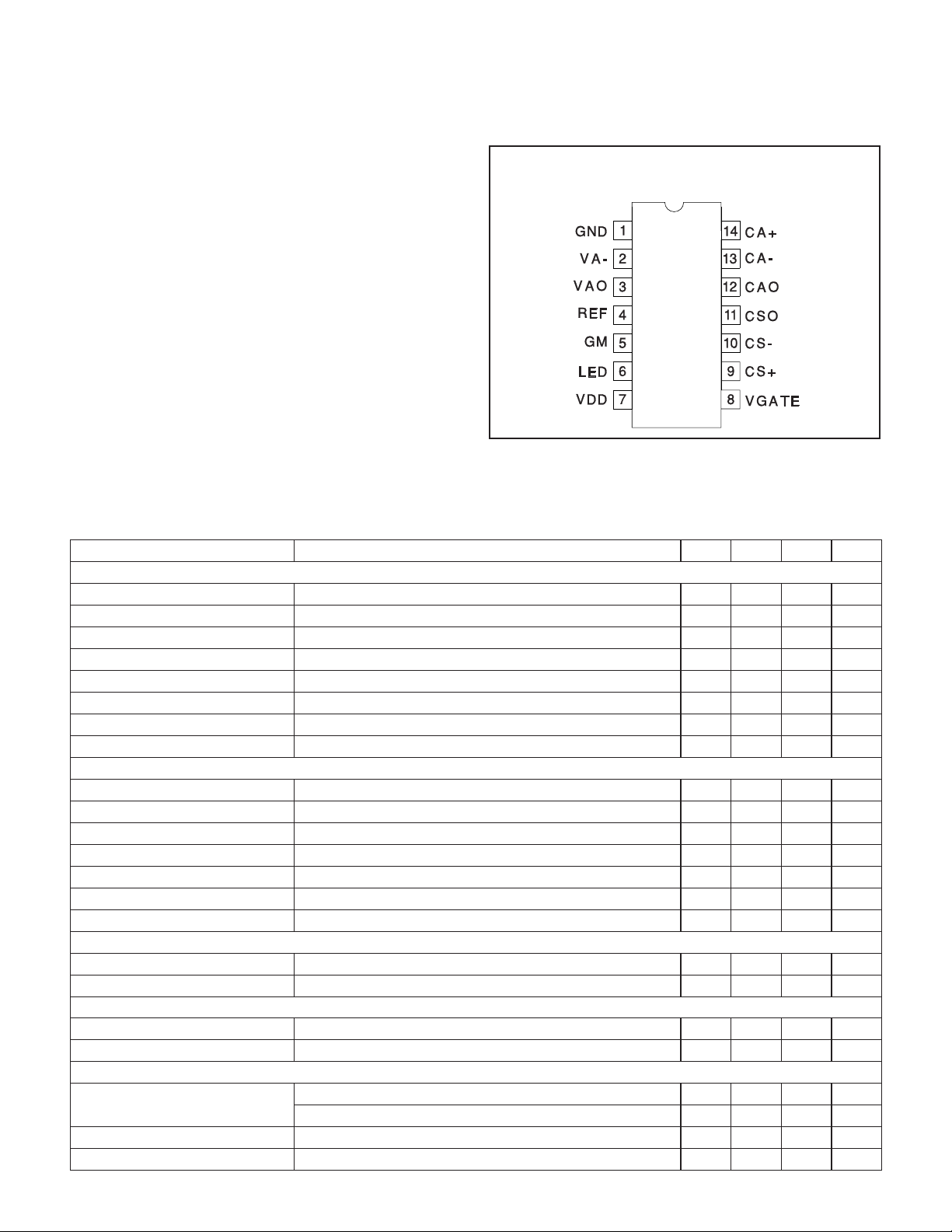
CONNECTION DIAGRAMS
DIL-14, SOIC-14 (Top View)
J or N Package, D Package
ELECTRICAL CHARACTERISTICS:
UCC2839 and –55°C to 125°C for the UCC1839. V
PARAMETER TEST CONDITIONS MIN TYP MAX UNITS
Current Error Amplifier
VIO 10 mV
AVOL 60 dB
CMRR V
PSRR VLINE = 10V to 20V 60 dB
CAO High CA– = 1V, CA+ = 1.1V, ICAO = –100µA 4.8 7 V
ICAO CA– = 1V, CA+ = 1.1V, CAO = 0.5V –500 –250 µA
CAO Low CA– = 1V, CA+ = 0.9V, ICAO = 500µA 0.2 0.4 V
GBW F = 100kHz, TA = 25°C 3 5 MHz
Voltage Error Amplifier
VA– 1.475 1.5 1.525 V
AVOL 60 dB
PSRR V
VAO High IVAO = –100µA to 100µA 4.8 5 5.2 V
IVAO VA– = 1.45V, VAO = 0.5V –500 –250 µA
VAO Low VA– = 1.55V, VAO = 0.5V, IVAO = 500µA 0.2 0.4 V
GBW (Note 1) 3 5 MHz
Current Sense Amplifier
CSO Zero CS+ = CS– = –0.3V to 5.5V, I
AV CS+ = 0, CS– = 0mV to –200mV 7.8 8 8.2 V/V
Current Sense Amplifier (cont.)
Slew Rate CS+ = 0, CS– = 0mV to –0.5V 2 4 V/µs
CSO CS+ = –200mV, CS– = –700mV 4.8 5 5.2 V
LED Driver
I
LED LED = 5.5V, CA– = 1V, CA+ = 1.1V, RG = 400 0 10 µA
Gm LED = 5.5V, CAO = 1V to 3V, RG = 400 2.25 2.5 2.75 mS
Slew Rate CAO = 2V to 2.5V, LED = 400Ω to 5.5V, RG = 400 2 4 V/µs
CM = 0.5V to 5.5V 60 dB
LINE = 10V to 20V 60 dB
LED = 5.5V, CA– = 1V, CA+ = 0.9V, RG = 400 9 10 11 mA
Unless otherwise specified, 0°C to 70°C for the UCC3839, –40°C to 85° for the
= 10V, RG = 400Ω. TA=TJ.
LINE
CSO = –100µA to 100µA 0.95 1 1.05 V
2
 Loading...