

查询UCC1570供应商
Low Power Pulse Width Modulator
UCC1570
UCC2570
UCC3570
FEATURES
• Low Power BiCMOS Process
• 85µA Start-up Current
• 1mA Run Current
• 1A Peak Gate Drive Output
• Voltage Feed Forward
• Programmable Duty Cycle Clamp
• Optocoupler Interface
• 500kHz Operation
• Soft Start
• Fault Counting Shutdown
• Fault Latch Off or Automatic Restart
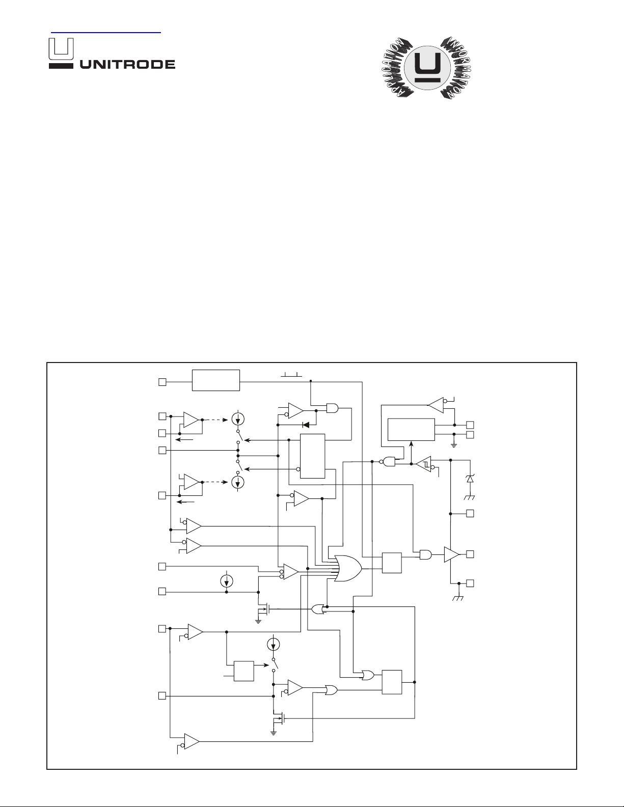
BLOCK DIAGRAM
1V
4V
1V
CLOCK
GENERATOR
I3
I4
HIGH
LINE
LOW
LINE
FREQ
VFWD
SLOPE
RAMP
ISET
FEEDBK
SOFTST
11
6
7
10
9
8
14
DESCRIPTION
The UCC1570 family of pulse width modulators is intended for application
in isolated switching supplies using primary side control and a voltage
mode feedback loop.Made with a BiCMOS process, these devices feature
low startup current for efficient off-line starting with a bootstrapped low voltage supply. Operating current is also very low; yet these devices maintain
the ability to drive a power MOSFET gate at frequencies above 500kHz.
Voltage feedforward provides fast and accurate response to wide line voltage variation without the noise sensitivity of current mode control. Fast current limiting is included with the ability to latch off after a programmable
number of repetitive faults has occurred. This allows the power supply to
ride through a temporary overload, while still shutting down in the event of
a permanent fault. Additional versatility is provided with a maximum duty
cycle clamp programmable within a 20% to 80% range and line voltage
sensing with a programmable window of allowable operation.
CLK
13/9V
4.5V
VREF
12
GND
13
15V
3
VCC
OUT
4
5
PGND
RAMP
VALLEY
1V
10 I3
S
RAMP
LATCH
R
10 I4
RAMP
PEAK
4V
I4
PWM
5V
GENERATOR
S
D
R
PWM
LATCH
04/99
CURLIM
COUNT
CURRENT
0.2V
LIMIT
CLK
SHUTDOWN
I4
SD
R
4V
R
D
S
SHUTDOWN
LATCH
2
1
0.6V
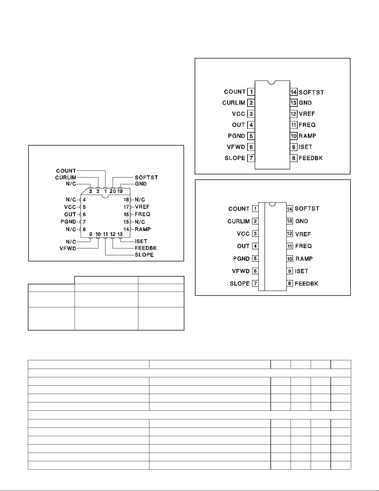
ABSOLUTE MAXIMUM RATINGS CONNECTION DIAGRAMS
Supply Voltage
(Limit Supply Current to 20mA) . . . . . . . Self Limiting at 15V
Supply Current . . . . . . . . . . . . . . . . . . . . . . . . . . . . . . . . . . . +20mA
Analog Inputs (CURLIM, VFWD, FEEBK) . . . . . . . . . . . . . . 6V
Programming Current I
Output Current I
OUT
SLOPE,IISET
. . . . . . . . . . . . . . . . . –1mA
DC . . . . . . . . . . . . . . . . . . . . . . . . . . . . . . . . . . . . . ±180mA
Pulse (0.5ms) . . . . . . . . . . . . . . . . . . . . . . . . . . . . . . . ±1.2A
Note: All voltages are with respect to GND. Currents are positive into the specified terminal. Consult Packaging Section of
Databook for thermal limitations and considerations of package.
PLCC-20 (TOP VIEW)
Q Package
DIL-14 (TOP VIEW)
N or J Package
SOIC-14 (TOP VIEW)
D Package
UCC1570
UCC2570
UCC3570
ORDERING INFORMATION
Temperature Range Package
UCC1570J –55°C to +125°C Ceramic Dip
UCC2570D –40°C to +85°C SOIC
UCC2750N Plastic Dip
UCC3570D 0°C to +70°C SOIC
UCC3570N Plastic Dip
UCC3570Q PLCC
ELECTRICAL CHARACTERISTICS: Unless otherwise stated, these specifications apply for T
UCC3570, TA= –40 to 85°C for the UCC2570, TA=–55 to 125°C for the UCC1570, R
C
=150pF, VCC=11V and TA=TJ.
RAMP
PARAMETER TEST CONDITIONS Min Typ Max Units
Reference
VREF VCC =10 to 13V, I
= 0 to 2mA 4.9 5 5.1 V
VREF
Line Regulation VCC = 10 to 13V 2 10 mV
Load Regulation I
= 0 to 2mA 2 10 mV
VREF
Short Circuit Current VREF = 0 10 50 mA
VCC
Vth (On) 12 13 V
Vth (Off) 8 9 10 V
Hysteresis 345V
VCC I
Start VCC = 11V, VCC Comparator Off 85 150 µA
I
VCC
I
VCC Run
= 10mA 13.5 15 16 V
VCC
VCC Comparator On 1 1.5 mA
ISET
=100k, R
= 0 to 70°C for the
A
=121k, C
SLOPE
FREQ
=180pF,
2
UCC1570
UCC2570
UCC3570
ELECTRICAL CHARACTERISTICS:
UCC3570, TA= –40 to 85°C for the UCC2570, TA=–55 to 125°C for the UCC1570, R
C
=150pF, VCC=11V and TA=TJ.
RAMP
PARAMETER TEST CONDITIONS Min Typ Max Units
Line Sense
Vth High Line Comparator 3.9 4 4.1 V
Vth Low Line Comparator 0.96 1 1.04 V
lib (VFWD) 0 ±100 nA
Oscillator
Frequency 90 100 110 kHz
Ramp Generator
I
RAMP/ISLOPE
–I
RAMP/IISET
Peak Ramp Voltage 3.8 4 4.2 V
Valley Ramp Voltage 0.95 1 1.05 V
ISET Voltage Level 0.95 1 1.05 V
Soft Start
Saturation VCC = 11V, VCC Comparator Off 25 100 mV
I
SOFTST/IISET
Pulse Width Modulator
lib(FEEDBK) 0 ±100 n A
FEEDBK Zero Duty Cycle 0.9 1 1.1 V
Current Limit
lib(CURLIM) 0 ±100 nA
Vth Current Limit 180 200 220 mV
Vth Shutdown 500 600 700 mV
Fault Counter
Vth 3.8 4 4.2 V
Vsat 0 100 mV
I
COUNT/IISET
Output Driver
Vsat High I
Vsat Low I
Rise/Fall Time C
Unless otherwise stated, these specifications apply for TA= 0 to 70°C for the
=100k, R
ISET
Maximum Duty Cycle, (Note 1) 3.8 4 4.2 V
= –100mA 0.4 1 V
OUT
= 100mA 0.4 1 V
OUT
= 1nF, (Note 1) 20 100 ns
OUT
=121k, C
SLOPE
9 10 11 A/A
9 10 11 A/A
0.8 1 1.2 A/A
0.8 1 1.2 A/A
FREQ
=180pF,
Note 1: This parameter guaranteed by design but not 100% tested in production.
PIN DESCRIPTIONS
VCC: Chip supply voltage pin. Bypass to PGND with a
low ESL/ESR 0.1µF capacitor plus a capacitor for gate
charge storage.Lead lengths must be minimum.
PGND: Ground pin for the output driver. Keep connections less than 2cm. Carefully maintain low impedance
path for high current return.
OUT: Gate drive output pin. Connect to the gate of a
power MOSFET with a resistor greater than 2Ω. Keep
connection lengths under 2cm.
VFWD: Voltage Feed Forward and Line Sense pin. Connect to input DC line using a resistive divider.
SLOPE: Program the charging current for RAMP with a
resistor from this pin to GND. This pin will follow VFWD.
FEEDBK: Input to the pulse width modulator comparator.
Drive this pin with an optocoupler to GND and a resistor
to VREF. Modulation input range is from 1V to 4V.
ISET: A resistor from this pin to GND programs RAMP
discharge current, FREQ current, SOFTST current, and
COUNT current.
3
 Loading...