

查询UCC1919供应商
3V to 8V Hot Swap Power Manager
FEATURES
Precision Fault Threshold
•
Charge Pump for Low RDS
•
Drive
Differential Sense Inputs
•
Programmable Average Power Limiting
•
Programmable Linear Current Control
•
Programmable Fault Time
•
Fault Output Indicator
•
Manual and Automatic Reset Modes
•
Shutdown Control w/Programmable
•
Softstart
Undervoltage Lockout
•
High Side
ON
DESCRIPTION
The UCC3919 family of Hot Swap Power Managers provide complete
power management, hot swap, and fault handling capability. The
UCC3919 features a duty ratio current limiting technique, which pro
vides peak load capability while limiting the average power dissipa
tion of the external pass transistor during fault conditions. The
UCC3919 has two reset modes, selected with the TTL/CMOS com
patible L/R pin. In one mode, when a fault occurs the IC repeatedly
tries to reset itself at a user defined rate, with user defined maximum
output current and pass transistor power dissipation. In the other
mode the output latches off and stays off until either the L/R pin is re
set or the shutdown pin is toggled. The on board charge pump circuit
provides the necessary gate voltage for an external N-channel power
FET.
application
INFO
available
UCC1919
UCC2919
UCC3919
-
-
-
-
• Electronic Circuit Breaker Function
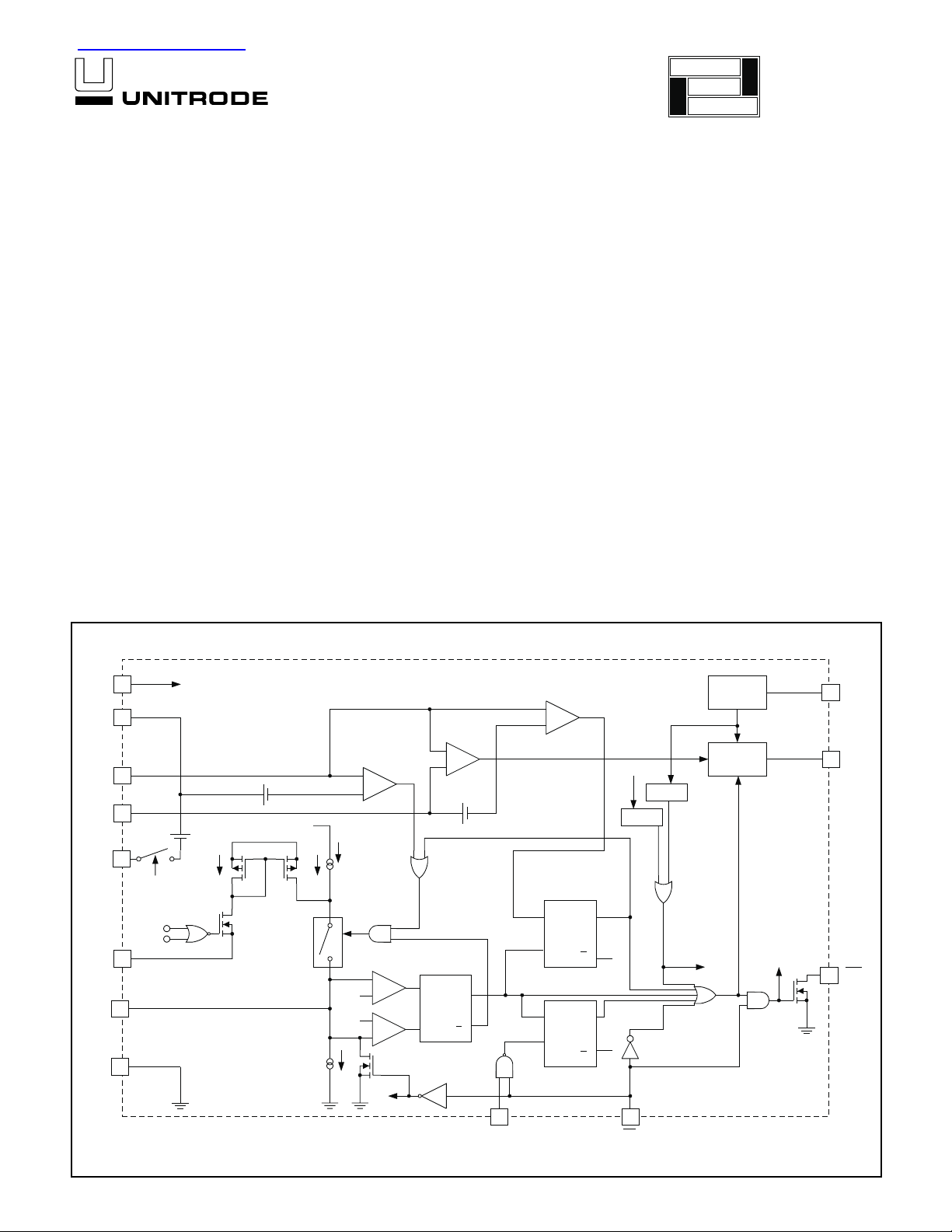
BLOCK DIAGRAM
13
VDD
14
CSP
12
CSN
1
IMAX
2
IBIAS
UVBIAS
9
PL
8
CT
11
GND
Note: Pins shown for 14-pin package.
07/99
FLT
SD
VDD
50mV
+
+
1.5v
1X
VDD
1X
OVERCURRENT
COMPARATOR
–
+
36µA
+
–
1.5V
0.5V
+
–
1.2µA
SD
LINEAR
CURRENT
AMPLIFIER
+
–
200mV
SRQ
OVERLOAD
COMPARATOR
+
DOMINANT
Q
DOMINANT
5 6
LR SD
–
+
SET
SRQ
SRQ
RESET
CHARGE
PUMP
UVBIAS
DRIVER
FLT
VDD
UVLO
UVLO
Q
Q
4
CAP
10
GATE
FLT
7
UDG-98123
ABSOLUTE MAXIMUM RATINGS
VDD. . . . . . . . . . . . . . . . . . . . . . . . . . . . . . . . . . . . –0.3V to 10V
Pin Voltage
(All pins except CAP and GATE). . . . . . –0.3V to VDD + 0.3V
Pin Voltage
(CAP and GATE) . . . . . . . . . . . . . . . . . . . . . . . . –0.3V to 15V
PL Current. . . . . . . . . . . . . . . . . . . . . . . . . . . . 0.5mA to –10mA
IBIAS Current. . . . . . . . . . . . . . . . . . . . . . . . . . . . . 0mA to 3mA
Storage Temperature . . . . . . . . . . . . . . . . . . . –65°C to +150°C
Junction Temperature. . . . . . . . . . . . . . . . . . . –55°C to +150°C
Lead Temperature (Soldering, 10sec.) . . . . . . . . . . . . . +300°C
Currents are positive into, negative out of the specified termi
nal. Consult Packaging Section ofDatabook for thermal limita
tions and considerations of package.
-
-
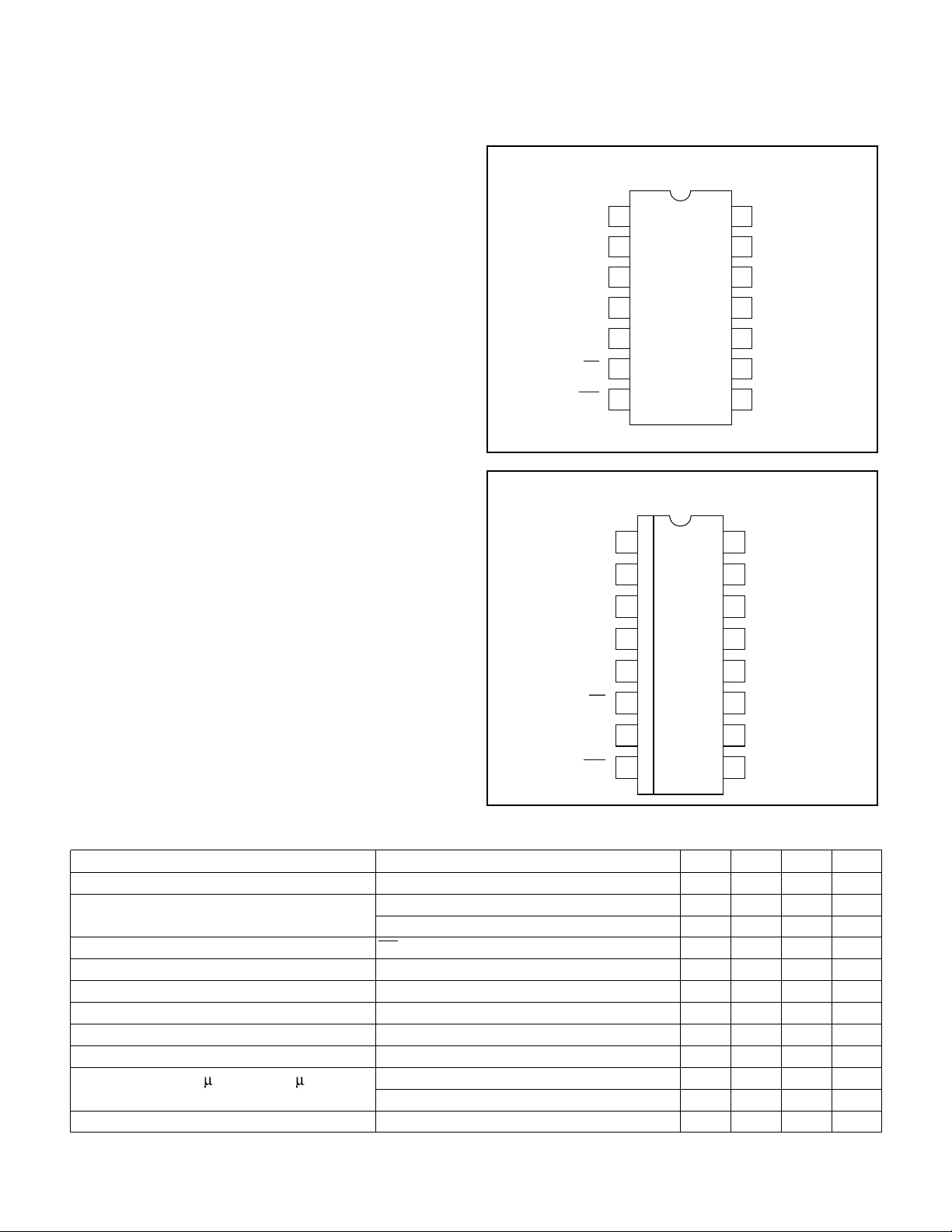
CONNECTION DIAGRAMS
DIL-14, (Top View)
N, J Packages
IMAX
1
IBIAS
2
N/C
3
CAP
4
L/R
5
SD
6
FLT
7
SOIC-16, TSSOP-16 (Top View)
D or PW Package
14
13
12
11
10
UCC1919
UCC2919
UCC3919
CSP
VDD
CSN
GND
GATE
PL
9
CT
8
16
15
14
13
12
11
10
9
A =TJ.
CSP
VDD
CSN
GND
GATE
PL
N/C
CT
ELECTRICAL CHARACTERISTICS:
IMAX
IBIAS
Unless otherwise specified, VDD = 5V, TA = 0°C to 70°C for the UCC3919, –40°C
N/C
CAP
L/R
SD
N/C
FLT
1
2
3
4
5
6
7
8
to 85°C for the UCC2919 and –55°C to 125°C for the UCC1919. All voltages are with respect to GND. T
PARAMETER TEST CONDITIONS MIN TYP MAX UNITS
Input Supply
Supply Current VDD = 3V 0.5 1 mA
VDD = 8V 1 1.5 mA
Shutdown Current SD
= 0.2V 1 7 µA
Undervoltage Lockout
Minimum Voltage to Start 2.35 2.75 3 V
Minimum Voltage after Start 1.9 2.25 2.5 V
Hysteresis 0.25 0.5 0.75 V
IBIAS
Output Voltage, (0
A < I
< 15 A) 25°C, referred to CSP 1.47 1.5 1.53 V
OUT
Over Temperature Range, referred to CSP 1.44 1.5 1.56 V
Maximum Output Current 12 mA
2
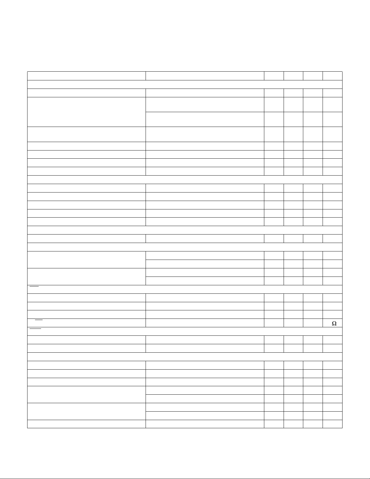
UCC1919
UCC2919
UCC3919
ELECTRICAL CHARACTERISTICS:
to 85°C for the UCC2919 and –55°C to 125°C for the UCC1919. All voltages are with respect to GND. T
Unless otherwise specified, VDD = 5V, TA = 0°C to 70°C for the UCC3919, –40°C
A =TJ.
PARAMETER TEST CONDITIONS MIN TYP MAX UNITS
Current Sense
Over Current Comparator Offset Referred to CSP, 3V ≤VDD ≤8V –55 –50 –45 mV
Linear Current Amplifier Offset V
= 100mV, Referred to CSP,
IMAX
–120 –100 –80 mV
3V ≤VDD ≤8V
= 400mV, Referred to CSP,
V
IMAX
–440 –400 –360 mV
3V ≤VDD ≤8V
Overload Comparator Offset V
= 100mV, Referred to CSP,
IMAX
–360 –300 –240 mV
3V ≤VDD ≤8V
CSN Input Common Mode Voltage Range Referred to VDD, 3V ≤VDD ≤ 8V, (Note 1) –1.5 0.2 V
CSP Input Common Mode Voltage Range Referred to VDD, 3V ≤VDD ≤8V, (Note 1) 0 0.2 V
Input Bias Current CSN 15µA
Input Bias Current CSP 100 200 µA
Current Fault Timer
CT Charge Current V
CT Discharge Current V
On Time Duty Cycle in Fault I
= 1V –56 –35 –16 µA
CT
= 1V 0.5 1.2 1.9 µA
CT
= 0 1.5 3 6 %
PL
CT Fault Threshold 1.0 1.5 1.7 V
CT Reset Threshold 0.25 0.5 0.75 V
IMAX
Input Bias Current V
= 100mV, Referred to CSP –1 0 1 µA
IMAX
Power Limiting Section
Voltage on PL I
On Time Duty Cycle in Fault I
SD
and L/R Inputs
= –250µA, Referred to VDD –1.0 –1.4 –1.9 V
PL
= –1.5mA, Referred to VDD –0.5 –1.8 –2.2 V
I
PL
= –250µA 0.25 0.5 1 %
PL
= –1.5mA 0.05 0.1 0.2 %
I
PL
Input Voltage Low 0.8 V
Input Voltage High 2V
L/R Input Current 136µA
Internal Pulldown Impedance 100 270 500 k
SD
FLT Output
Output Leakage Current VDD = 5V 10 µA
Output Low Voltage I
= 10mA 1 V
OUT
FET GATE Driver and Charge Pump
Peak Output Current V
Peak Sink Current V
= +15V, V
CAP
= 5V 20 mA
GATE
= 10V –3 –1 –0.25 mA
GATE
Fault Delay 100 300 nS
Maximum Output Voltage VDD = 3V, Average I
VDD = 8V, Average I
Charge Pump UVLO Minimum Voltage to
Start
VDD = 3V 6.5 7.5 V
VDD = 8V 6.5 8 V
Charge Pump Source Impedance VDD = 5V, Average I
= 1µA 8 10 12 V
OUT
= 1µA 121416 V
OUT
= 1µA 50 100 150 kΩ
OUT
Note 1: Guaranteed by design.Not 100% tested in production.
3

PIN DESCRIPTIONS
CAP: A capacitor is placed from this pin to ground to fil
ter the output of the on board charge pump. A .01µFto
0.1µF capacitor is recommended .
CSN: The negative current sense input signal.
CSP: The positive current sense input signal.
CT: Input to the duty cycle timer. A capacitor is con
nected from this pin to ground, setting the off time and
the maximum on time of the overcurrent protection cir
cuits.
FLT
: Fault indicator. This open drain output will pull low
under any fault condition where the output driver is dis
abled. This output is disabled when the IC is in low cur
rent standby mode.
GATE: The output of the linear current amplifier. This pin
drives the gate of an external N-channel MOSFET pass
transistor. The linear current amplifier control loop is in
ternally compensated, and guaranteed stable for output
load (gate) capacitance between 100pF and .01µF. In
applications where the GATE voltage (or charge pump
voltage) exceeds the maximum Gate-to-Source voltage
ratings (V
Zener clamp may be added to the gate of the MOSFET.
No additional series resistance is required since the internal charge pump has a finite output impedance of
100k
GND: The ground reference for the device.
IBIAS: Output of the on board bias generator internally
regulated to 1.5V below CSP. A resistor divider between
this pin and CSP can be used to generate the IMAX volt
age. The bias circuit is internally compensated, and re
quires no bypass capacitance. If an external bypass is
required due to a noisy environment, the circuit will be
) for the external N-channel MOSFET, a
GS
typical.
UCC1919
UCC2919
UCC3919
-
stable with up to .001µF of capacitance. The bypass
must be to CSP, since the bias voltage is generated with
respect to CSP. Resistor R2 (Figure 4) should be greater
than 50k
ance of the IBIAS pin on the IMAX threshold.
IMAX: Used to program the maximum allowable sourcing
-
current. The voltage on this pin is with respect to CSP. If
the voltage across the shunt resistor exceeds this voltage
-
the linear current amplifier lowers the voltage at GATE to
limit the output current to this level. If the voltage across
the shunt resistor goes more than 200mV beyond this
voltage, the gate drive pin GATE is immediately driven
low and kept low for one full off time interval.
L/R: Latch/Reset. This pin sets the reset mode. If L/R is
low and a fault occurs the device will begin duty ratio cur
rent limiting. If L/R is high and a fault occurs, GATE will
go low and stay low until L/R is set low. This pin is inter
nally pulled low by a 3µA nominal pulldown.
PL: Power Limit. This pin is used to control average
power dissipation in the external MOSFET.If a resistor is
connected from this pin to the source of the external
MOSFET, the current in the resistor will be roughly proportional to the voltage across the FET. As the voltage
across the FET increases, this current is added to the
fault timer charge current, reducing the on time duty cycle from its nominal value of 3% and limiting the average
power dissipation in the FET.
: Shutdown pin. If this pin is taken low, GATE will go
SD
low, and the IC will go into a low current standby mode
and CT will be discharged. This TTL compatible input
must be driven high to turn on.
VDD: The power connection for the device.
to minimize the effect of the finite input imped
-
-
-
APPLICATION INFORMATION
The UCC3919 monitors the voltage drop across a high
side sense resistor and compares it against three differ
ent voltage thresholds. These are discussed below. Fig
ure 1 shows the UCC3919 waveforms under fault
conditions.
Fault Threshold
The first threshold is fixed at 50mV. If the current is high
enough such that the voltage on CSN is 50mV below
CSP, the timing capacitor C
35µA if the PL pin is open. (Power limiting will be dis
cussed later). If this threshold is exceeded long enough
to charge to 1.5V, a fault is declared and the exter
for C
T
T begins to charge at about
nal MOSFET will be turned off. It will either be latched off
-
(until the power to the circuit is cycled, the L/R pin is
-
taken low, or the SD
fixed off time (when C
pin is toggled), or will retry after a
T has discharged to 0.5V), depend
ing on whether the L/R pin is set high or low by the user.
The equation for this current threshold is simply:
I
FAULT
The first time a fault occurs, C
charge 1.5V. Therefore:
-
tt
FAULT ON
005.
=
R
SENSE
CF
()
==
(sec)
T
35
T is at ground, and must
•
.µ 15
4
-
(1)
(2)
 Loading...